Q24S25015 DC-DC Converter Data Sheet - Power-One
Q24S25015 DC-DC Converter Data Sheet - Power-One
Q24S25015 DC-DC Converter Data Sheet - Power-One

You also want an ePaper? Increase the reach of your titles
YUMPU automatically turns print PDFs into web optimized ePapers that Google loves.
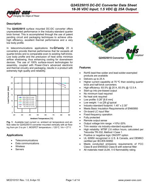
<strong>Q24S25015</strong> <strong>DC</strong>-<strong>DC</strong> <strong>Converter</strong> <strong>Data</strong> <strong>Sheet</strong>18-36 V<strong>DC</strong> Input; 1.5 V<strong>DC</strong> @ 25A OutputDescriptionThe <strong>Q24S25015</strong> surface mounted <strong>DC</strong>-<strong>DC</strong> converter offersunprecedented performance in the industry-standard quarterbrick format. This is accomplished through the use of patentpending circuit and packaging techniques to achieve ultrahighefficiency, excellent thermal performance and a verylow body profile.In telecommunications applications the Q Family 25 Aconverters provide thermal performance that far exceeds allquarter-bricks and is comparable even to existing half-bricks.Low body profile and the preclusion of heat sinks minimizeairflow shadowing, thus enhancing cooling for downstreamdevices. The use of 100% surface-mount technologies forassembly, coupled with <strong>Power</strong>-<strong>One</strong>’s advanced electronicand thermal circuitry and packaging, results in a product withextremely high quality and reliability.Load Current [Adc]30252015105500 LFM (2.5 m/s)400 LFM (2.0 m/s)300 LFM (1.5 m/s)200 LFM (1.0 m/s)100 LFM (0.5 m/s)30 LFM (0.15 m/s)020 30 40 50 60 70 80 90Ambient Temperature [°C]Fig. 1: Available load current vs. ambient air temperature and airflowrates for <strong>Q24S25015</strong> converter mounted vertically with air flowingfrom pin 3 to pin 1, MOSFET temperature 120C, Vin = 27 V.ApplicationsTelecommunications<strong>Data</strong> communicationsWirelessServers<strong>Q24S25015</strong> <strong>Converter</strong>Features RoHS lead-free solder and lead-solder-exemptedproducts are available Delivers up to 25 A Higher current capability at 70 ºC than existing quarterbrick and half-brick converters High efficiency: 83.5% @ 25 A, 83.5% @ 12.5 A Start-up into pre-biased output No minimum load required No heat sink required Low profile: 0.26” [6.6 mm] Low weight: 1 oz [28 g] typical Industry-standard footprint: 1.45” x 2.30” Meets Basic Insulation Requirements of EN60950 On-board LC input filter Fixed-frequency operation Fully protected Remote output sense Output voltage trim range: +10%/-20% Trim resistor via industry-standard equations High reliability: MTBF 2.6 million hours, calculated perTelcordia TR-332, Method I Case 1 Positive or negative logic ON/OFF option UL 60950 recognized in U.S. & Canada, and DEMKOcertified per IEC/EN 60950 Meets conducted emissions requirements of FCCClass B and EN55022 Class B with external filter All materials meet UL94, V-0 flammability ratingMCD10151 Rev. 1.0, 6-Apr-10 Page 1 of 14 www.power-one.com
<strong>Q24S25015</strong> <strong>DC</strong>-<strong>DC</strong> <strong>Converter</strong> <strong>Data</strong> <strong>Sheet</strong>18-36 V<strong>DC</strong> Input; 1.5 V<strong>DC</strong> @ 25A OutputElectrical SpecificationsConditions: T A =25 ºC, Airflow=300 LFM (1.5 m/s), Vin=24 V<strong>DC</strong>, unless otherwise specified.PARAMETER NOTES MIN TYP MAX UNITSABSOLUTE MAXIMUM RATINGSInput Voltage Continuous 0 40 V<strong>DC</strong>Operating Ambient Temperature -40 85 °CStorage Temperature -55 125 °CINPUT CHARACTERISTICSOperating Input Voltage Range 18 24 36 V<strong>DC</strong>Input Under Voltage LockoutNon-latchingTurn-on Threshold 16 17 17.5 V<strong>DC</strong>Turn-off Threshold 15 16 16.5 V<strong>DC</strong>OUTPUT CHARACTERISTICSExternal Load Capacitance Plus full load (resistive) 30,000 μFOutput Current Range 0 25 A<strong>DC</strong>Current Limit Inception Non-latching 26 30 35 A<strong>DC</strong>Peak Short-Circuit Current Non-latching. Short=10mΩ. 35 46 ARMS Short-Circuit Current Non-latching 6.7 ArmsISOLATION CHARACTERISTICSI/O Isolation 2000 V<strong>DC</strong>Isolation Capacitance 230 ρFIsolation Resistance 10 MΩFEATURE CHARACTERISTICSSwitching Frequency 435 kHzOutput Voltage Trim Range 1 Use trim equations on Page 6 -20 +10 %Remote Sense Compensation 1 Percent of V OUT (NOM) +10 %Output Over-Voltage Protection Non-latching 117 122 127 %Over-Temperature Shutdown (PCB) Non-latching 118 °CAuto-Restart Period Applies to all protection features 100 msTurn-On Time 2.5 msON/OFF Control (Positive Logic)<strong>Converter</strong> Off -20 0.8 V<strong>DC</strong><strong>Converter</strong> On 2.4 20 V<strong>DC</strong>ON/OFF Control (Negative Logic)<strong>Converter</strong> Off 2.4 20 V<strong>DC</strong><strong>Converter</strong> On -20 0.8 V<strong>DC</strong>Additional Notes:1. Vout can be increased up to 10% via the sense leads or up to 10% via the trim function, however total output voltage trim from all sourcesshould not exceed 10% of V OUT (NOM), in order to insure specified operation of over-voltage protection circuitry. See further discussion at end ofOutput Voltage Adjust /TRIM section.MCD10151 Rev. 1.0, 6-Apr-10 Page 2 of 14 www.power-one.com
<strong>Q24S25015</strong> <strong>DC</strong>-<strong>DC</strong> <strong>Converter</strong> <strong>Data</strong> <strong>Sheet</strong>18-36 V<strong>DC</strong> Input; 1.5 V<strong>DC</strong> @ 25A OutputElectrical Specifications (continued)Conditions: T A =25 ºC, Airflow=300 LFM (1.5 m/s), Vin=24 V<strong>DC</strong>, unless otherwise specified.PARAMETER NOTES MIN TYP MAX UNITSINPUT CHARACTERISTICSMaximum Input Current 25 A<strong>DC</strong>, 1.5 V<strong>DC</strong> Out @ 18 V<strong>DC</strong> In 2.5 A<strong>DC</strong>Input Stand-by Current Vin = 24 V, converter disabled 3.5 mA<strong>DC</strong>Input No Load Current (0 load on the output) Vin = 24 V, converter enabled 80 mA<strong>DC</strong>Input Reflected-Ripple Current See Figure 25 - 25MHz bandwidth 6 mA PK-PKInput Voltage Ripple Rejection 120Hz TBD dBOUTPUT CHARACTERISTICSOutput Voltage Set Point (no load) -40ºC to 85ºC 1.485 1.500 1.515 V<strong>DC</strong>Output RegulationOver Line ±2 ±4 mVOver Load ±2 ±4 mVOutput Voltage Range Over line, load and temperature 1.477 1.523 V<strong>DC</strong>Output Ripple and Noise - 25MHz bandwidth Full load + 10 μF tantalum + 1 μF ceramic 30 50 mV PK-PKDYNAMIC RESPONSELoad Change 25% of Iout Max, di/dt = 0.1 A/μS Co = 1 μF ceramic (Fig.20) 50 mVdi/dt = 5 A/μS Co = 450 μF tant. + 1 μF ceramic (Fig.21) 140 mVSetting Time to 1% 100 µsEFFICIENCY100% Load 83.5 %50% Load 83.5 %MCD10151 Rev. 1.0, 6-Apr-10 Page 3 of 14 www.power-one.com
<strong>Q24S25015</strong> <strong>DC</strong>-<strong>DC</strong> <strong>Converter</strong> <strong>Data</strong> <strong>Sheet</strong>18-36 V<strong>DC</strong> Input; 1.5 V<strong>DC</strong> @ 25A OutputPhysical Information187TOP VIEW2 653 4SIDE VIEWPin ConnectionsPin #Function1 Vin (+)2 ON/OFF3 Vin (-)4 Vout (-)5 SENSE(-)6 TRIM7 SENSE(+)8 Vout (+)All dimensions are in inches [mm]Connector Material: CopperConnector Finish: Gold over Nickel<strong>Converter</strong> Weight: 1 oz [28 g] typicalRecommended Surface-Mount Pads:Min. 0.080” x 0.112” [2.03 x 2.84]Max. 0.092” x 0.124” [2.34 x 3.15]<strong>Converter</strong> Part Numbering SchemeProductSeriesInputVoltageMountingSchemeRatedLoadCurrentOutputVoltageON/OFF LogicMaximumHeightPinLengthQ 24 S 25 015 - N S 0 0SpecialFeaturesQuarter-BrickFormat18-36 VSurfaceMount25 A<strong>DC</strong> 015 1.5 VN NegativeP PositiveS 0.273” 0 0.00” 0 STDThe example above describes P/N <strong>Q24S25015</strong>-NS00: 18-36 V input, surface mounting, 25 A @ 1.5 V output, negative ON/OFF logic. Pleaseconsult factory regarding availability of a specific version.RoHS Ordering Information:No RoHS suffix character is required for lead-solder-exemption compliance.For RoHS compliance to all six substances, add the letter "G" as the last letter of the part number.Model numbers highlighted in yellow or shaded are not recommended for new designs.MCD10151 Rev. 1.0, 6-Apr-10 Page 4 of 14 www.power-one.com
<strong>Q24S25015</strong> <strong>DC</strong>-<strong>DC</strong> <strong>Converter</strong> <strong>Data</strong> <strong>Sheet</strong>18-36 V<strong>DC</strong> Input; 1.5 V<strong>DC</strong> @ 25A OutputOperationInput and Output ImpedanceThese power converters have been designed to be stablewith no external capacitors when used in low inductance inputand output circuits.However, in many applications, the inductance associatedwith the distribution from the power source to the input of theconverter can affect the stability of the converter. The additionof a 33 µF electrolytic capacitor with an ESR < 1 across the input helps ensure stability of the converter. Inmany applications, the user has to use decoupling capacitanceat the load. The power converter will exhibit stable operationwith external load capacitance up to 30,000 µF.ON/OFF (Pin 2)The ON/OFF pin is used to turn the power converter on oroff remotely via a system signal. There are two remote controloptions available, positive logic and negative logic andboth are referenced to Vin(-). Typical connections are shownin Fig. 2.VinCONTROLINPUTVin (+)ON/OFFVin (-)TMQ Family<strong>Converter</strong>(Top View)Vout (+)SENSE (+)TRIMSENSE (-)Vout (-)Fig. 2: Circuit configuration for ON/OFF function.The positive logic version turns on when the ON/OFF pin isat logic high and turns off when at logic low. The converter ison when the ON/OFF pin is left open.The negative logic version turns on when the pin is at logiclow and turns off when the pin is at logic high. The ON/OFFpin can be hard wired directly to Vin(-) to enable automaticpower up of the converter without the need of an externalcontrol signal.ON/OFF pin is internally pulled-up to 5 V through a resistor.A mechanical switch, open collector transistor, or FET canbe used to drive the input of the ON/OFF pin. The devicemust be capable of sinking up to 0.2 mA at a low level voltageof 0.8 V. An external voltage source of ±20 V max.may be connected directly to the ON/OFF input, in whichRloadcase it should be capable of sourcing or sinking up to 1 mAdepending on the signal polarity. See the Start-up Informationsection for system timing waveforms associated withuse of the ON/OFF pin.Remote Sense (Pins 5 and 7)The remote sense feature of the converter compensates forvoltage drops occurring between the output pins of the converterand the load. The SENSE(-) (Pin 5) and SENSE(+)(Pin 7) pins should be connected at the load or at the pointwhere regulation is required (see Fig. 3).VinVin (+)ON/OFFVin (-)TMQ Family<strong>Converter</strong>(Top View)Vout (+)100SENSE (+)TRIMSENSE (-)10Vout (-)Fig. 3: Remote sense circuit configuration.If remote sensing is not required, the SENSE(-) pin must beconnected to the Vout(-) pin (Pin 4), and the SENSE(+) pinmust be connected to the Vout(+) pin (Pin 8) to ensure theconverter will regulate at the specified output voltage. Ifthese connections are not made, the converter will deliver anoutput voltage that is slightly higher than the specified value.Because the sense leads carry minimal current, large traceson the end-user board are not required. However, sensetraces should be located close to a ground plane to minimizesystem noise and insure optimum performance. When wiringdiscretely, twisted pair wires should be used to connect thesense lines to the load to reduce susceptibility to noise.The converter’s output over-voltage protection (OVP) sensesthe voltage across Vout(+) and Vout(-), and not across thesense lines, so the resistance (and resulting voltage drop)between the output pins of the converter and the load shouldbe minimized to prevent unwanted triggering of the OVP.When utilizing the remote sense feature, care must be takennot to exceed the maximum allowable output power capabilityof the converter, equal to the product of the nominal outputvoltage and the allowable output current for the givenconditions.RwRwRloadMCD10151 Rev. 1.0, 6-Apr-10 Page 5 of 14 www.power-one.com
<strong>Q24S25015</strong> <strong>DC</strong>-<strong>DC</strong> <strong>Converter</strong> <strong>Data</strong> <strong>Sheet</strong>18-36 V<strong>DC</strong> Input; 1.5 V<strong>DC</strong> @ 25A OutputWhen using remote sense, the output voltage at the convertercan be increased by as much as 10% above the nominalrating in order to maintain the required voltage across theload. Therefore, the designer must, if necessary, decreasethe maximum current (originally obtained from the deratingcurves) by the same percentage to ensure the converter’sactual output power remains at or below the maximum allowableoutput power.VinVin (+)ON/OFFVin (-)TMQ Family<strong>Converter</strong>(Top View)Vout (+)SENSE (+)TRIMSENSE (-)Vout (-)R T-INCRRloadOutput Voltage Adjust /TRIM (Pin 6)The converter’s output voltage can be adjusted up 10% ordown 20% relative to the rated output voltage by the additionof an externally connected resistor.The TRIM pin should be left open if trimming is not beingused. To minimize noise pickup, a 0.1 µF capacitor is connectedinternally between the TRIM and SENSE(-) pins.To increase the output voltage, refer to Fig. 4. A trim resistor,R T-INCR , should be connected between the TRIM (Pin 6) andSENSE(+) (Pin 7), with a value of:5.11(100 Δ)VONOM 626RT INCR 10.22 [k]1.225Δwhere,RTINCRVONOM Required value of trim-up resistor k]Nominal value of output voltage [V](VO-REQ VO-NOM)Δ X 100 [%]VO -NOMVOREQ Desired (trimmed) output voltage [V].When trimming up, care must be taken not to exceed theconverter‘s maximum allowable output power. See previoussection for a complete discussion of this requirement.To decrease the output voltage (Fig. 5), a trim resistor,R T-DECR , should be connected between the TRIM (Pin 6) andSENSE(-) (Pin 5), with a value of:Fig. 4: Configuration for increasing output voltage.RTDECR Required value of trim-down resistor [k]and Δ is as defined above.Note: The above equations for calculation of trim resistorvalues match those typically used in conventional industrystandardquarter bricks.VinVin (+)ON/OFFVin (-)TMQ Family<strong>Converter</strong>(Top View)Vout (+)SENSE (+)TRIMSENSE (-)Vout (-)RT-DECRFig. 5: Configuration for decreasing output voltage.Trimming/sensing beyond 110% of the rated output voltageis not an acceptable design practice, as this condition couldcause unwanted triggering of the output over-voltage protection(OVP) circuit. The designer should ensure that the differencebetween the voltages across the converter’s outputpins and its sense pins does not exceed 0.15 V, or:[VOUT( ) VOUT()] [VSENSE() VSENSE()] 0.15 [V]This equation is applicable for any condition of output sensingand/or output trim.Rload511RT DECR 10.22 [k]Δwhere,MCD10151 Rev. 1.0, 6-Apr-10 Page 6 of 14 www.power-one.com
<strong>Q24S25015</strong> <strong>DC</strong>-<strong>DC</strong> <strong>Converter</strong> <strong>Data</strong> <strong>Sheet</strong>18-36 V<strong>DC</strong> Input; 1.5 V<strong>DC</strong> @ 25A OutputProtection FeaturesInput Undervoltage LockoutInput undervoltage lockout is standard with this converter.The converter will shut down when the input voltage dropsbelow a pre-determined voltage.The input voltage must be at least 35 V for the converter toturn on. Once the converter has been turned on, it will shutoff when the input voltage drops below 31 V. This feature isbeneficial in preventing deep discharging of batteries used intelecom applications.Output Overcurrent Protection (OCP)The converter is protected against overcurrent or short circuitconditions. Upon sensing an overcurrent condition, theconverter will switch to constant current operation and therebybegin to reduce output voltage. When the output voltagedrops below 0.7 V<strong>DC</strong>, the converter will shut down (Fig. 26).Once the converter has shut down, it will attempt to restartnominally every 100 ms with a 3% duty cycle (Fig 27). Theattempted restart will continue indefinitely until the overloador short circuit conditions are removed or the output voltagerises above 0.7 V<strong>DC</strong>.Safety RequirementsThe converters meet North American and International safetyregulatory requirements per UL60950 and EN60950. BasicInsulation is provided between input and output.To comply with safety agencies requirements, an input linefuse must be used external to the converter. A 5-A fuse isrecommended for use with this product.Electromagnetic Compatibility (EMC)EMC requirements must be met at the end-product systemlevel, as no specific standards dedicated to EMC characteristicsof board mounted component dc-dc converters exist.However, <strong>Power</strong>-<strong>One</strong> tests its converters to several systemlevel standards, primary of which is the more stringentEN55022, Information technology equipment - Radio disturbancecharacteristics - Limits and methods of measurement.With the addition of a simple external filter (see applicationnotes), all versions of the Q24S25 converters pass the requirementsof Class B conducted emissions per EN55022and FCC, and meet at a minimum, Class A radiated emissionsper EN 55022 and Class B per FCC Title 47CFR, Part15-J. Please contact <strong>Power</strong>-<strong>One</strong> Applications Engineeringfor details of this testing.Output Overvoltage Protection (OVP)The converter will shut down if the output voltage acrossVout(+) (Pin 8) and Vout(-) (Pin 4) exceeds the threshold ofthe OVP circuitry. The OVP circuitry contains its own reference,independent of the output voltage regulation loop.Once the converter has shut down, it will attempt to restartevery 100 ms until the OVP condition is removed.Overtemperature Protection (OTP)The converter will shut down under an overtemperature conditionto protect itself from overheating caused by operationoutside the thermal derating curves, or operation in abnormalconditions such as system fan failure. After the converterhas cooled to a safe operating temperature, it will automaticallyrestart.MCD10151 Rev. 1.0, 6-Apr-10 Page 7 of 14 www.power-one.com
<strong>Q24S25015</strong> <strong>DC</strong>-<strong>DC</strong> <strong>Converter</strong> <strong>Data</strong> <strong>Sheet</strong>18-36 V<strong>DC</strong> Input; 1.5 V<strong>DC</strong> @ 25A OutputCharacterizationGeneral InformationThe converter has been characterized for many operationalaspects, to include thermal derating (maximum load currentas a function of ambient temperature and airflow) for verticaland horizontal mounting, efficiency, start-up and shutdownparameters, output ripple and noise, transient response toload step-change, overload and short circuit.The following pages contain specific plots or waveforms associatedwith the converter. Additional comments for specificdata are provided below.Test ConditionsAll data presented were taken with the converter soldered toa test board, specifically a 0.060” thick printed wiring board(PWB) with four layers. The top and bottom layers were notmetalized. The two inner layers, comprising two-ounce copper,were used to provide traces for connectivity to the converter.The lack of metalization on the outer layers as well as thelimited thermal connection ensured that heat transfer fromthe converter to the PWB was minimized. This provides aworst-case but consistent scenario for thermal derating purposes.All measurements requiring airflow were made in <strong>Power</strong>-<strong>One</strong>’s vertical and horizontal wind tunnel facilities usingInfrared (IR) thermography and thermocouples for thermometry.Ensuring components on the converter do not exceed theirratings is important to maintaining high reliability. If one anticipatesoperating the converter at or close to the maximumloads specified in the derating curves, it is prudent to checkactual operating temperatures in the application. Thermographicimaging is preferable; if this capability is not available,then thermocouples may be used. <strong>Power</strong>-<strong>One</strong> recommendsthe use of AWG #40 gauge thermocouples to ensuremeasurement accuracy. Careful routing of the thermocoupleleads will further minimize measurement error. Refer toFigure 28 for optimum measuring thermocouple location.Thermal DeratingLoad current vs. ambient temperature and airflow rates aregiven in Figs. 10-13. Ambient temperature was varied between25 °C and 85 °C, with airflow rates from 30 to 500LFM (0.15 to 2.5 m/s), and vertical and horizontal convertermounting.For each set of conditions, the maximum load current wasdefined as the lowest of:(i) The output current at which either any FET junction temperaturedid not exceed a maximum specified temperature(either 105 °C or 120 °C) as indicated by the thermographicimage, or(ii) The nominal rating of the converter (25 A)During normal operation, derating curves with maximum FETtemperature less than or equal to 120 °C should not be exceeded.Temperature on the PCB at the thermocouple locationshown in Fig. 28 should not exceed 118 °C in order tooperate inside the derating curves.EfficiencyEfficiency vs. load current plots are shown in Figs. 14 and 16for ambient temperature of 25 ºC, airflow rate of 300 LFM(1.5 m/s), both vertical and horizontal orientations, and inputvoltages of 18 V, 27 V and 36 V. Also, plots of efficiency vs.load current, as a function of ambient temperature with Vin =27 V, airflow rate of 200 LFM (1 m/s) are shown for both avertically and horizontally mounted converter in Figs. 15 and17, respectively.Start-upOutput voltage waveforms, during the turn-on transient usingthe ON/OFF pin for full rated load currents (resistive load)are shown without and with 10,000 F load capacitance inFigs. 18 and 19, respectively.Ripple and NoiseFigure 22 shows the output voltage ripple waveform,measured at full rated load current with a 10 µF tantalumand 1 µF ceramic capacitor across the output. Note that alloutput voltage waveforms are measured across a 1 Fceramic capacitor.The input reflected ripple current waveforms are obtainedusing the test setup shown in Fig 23. The correspondingwaveforms are shown in Figs. 24 and 25.MCD10151 Rev. 1.0, 6-Apr-10 Page 8 of 14 www.power-one.com
<strong>Q24S25015</strong> <strong>DC</strong>-<strong>DC</strong> <strong>Converter</strong> <strong>Data</strong> <strong>Sheet</strong>18-36 V<strong>DC</strong> Input; 1.5 V<strong>DC</strong> @ 25A OutputStart-up Information (using negative ON/OFF)VINScenario #1: Initial Start-up From Bulk SupplyON/OFF function enabled, converter started via application of V IN .See Figure 7.TimeCommentst 0 ON/OFF pin is ON; system front end power is toggledon, V IN to converter begins to rise.t 1 V IN crosses Under-Voltage Lockout protection circuitthreshold; converter enabled.t 2 <strong>Converter</strong> begins to respond to turn-on command(converter turn-on delay).t 3 <strong>Converter</strong> V OUT reaches 100% of nominal value.For this example, the total converter start-up time (t 3 - t 1 ) is typically2.5 ms.Scenario #2: Initial Start-up Using ON/OFF PinWith V IN previously powered, converter started via ON/OFF pin.See Figure 8.TimeCommentst 0 V INPUT at nominal value.t 1 Arbitrary time when ON/OFF pin is enabled (converterenabled).t 2 End of converter turn-on delay.t 3 <strong>Converter</strong> V OUT reaches 100% of nominal value.For this example, the total converter start-up time (t 3 - t 1 ) is typically2.5 ms.ON/OFFSTATEVOUTVINON/OFFSTATEVOUTOFFONt0 t1 t2 t3OFFONFig. 7: Start-up scenario #1.tScenario #3: Turn-off and Restart Using ON/OFF PinWith V IN previously powered, converter is disabled and thenenabled via ON/OFF pin. See Figure 9.TimeCommentst 0 V IN and V OUT are at nominal values; ON/OFF pin ON.t 1 ON/OFF pin arbitrarily disabled; converter output fallsto zero; turn-on inhibit delay period (100 ms typical) isinitiated, and ON/OFF pin action is internally inhibited.t 2 ON/OFF pin is externally re-enabled.If (t 2 - t 1 ) ≤ 100 ms, external action of ON/OFF pinis locked out by start-up inhibit timer.If (t 2 - t 1 ) > 100 ms, ON/OFF pin action is internallyenabled.t 3 Turn-on inhibit delay period ends. If ON/OFF pin is ON,converter begins turn-on; if off, converter awaitsON/OFF pin ON signal; see Figure 8.t 4 End of converter turn-on delay.t 5 <strong>Converter</strong> V OUT reaches 100% of nominal value.For the condition, (t 2 - t 1 ) ≤ 100 ms, the total converter start-uptime (t 5 - t 2 ) is typically 102.5 ms. For (t 2 - t 1 ) > 100 ms, start-up willbe typically 2.5 ms after release of ON/OFF pin.VINON/OFFSTATEVOUTOFFONt0 t1 t2 t3Fig. 8: Start-up scenario #2.100 mstt0t1t2t3 t4t5tFig. 9: Start-up scenario #3.MCD10151 Rev. 1.0, 6-Apr-10 Page 9 of 14 www.power-one.com
<strong>Q24S25015</strong> <strong>DC</strong>-<strong>DC</strong> <strong>Converter</strong> <strong>Data</strong> <strong>Sheet</strong>18-36 V<strong>DC</strong> Input; 1.5 V<strong>DC</strong> @ 25A Output30302525Load Current [Adc]2015105500 LFM (2.5 m/s)400 LFM (2.0 m/s)300 LFM (1.5 m/s)200 LFM (1.0 m/s)100 LFM (0.5 m/s)30 LFM (0.15 m/s)Load Current [Adc]2015105500 LFM (2.5 m/s)400 LFM (2.0 m/s)300 LFM (1.5 m/s)200 LFM (1.0 m/s)100 LFM (0.5 m/s)30 LFM (0.15 m/s)020 30 40 50 60 70 80 90Ambient Temperature [°C]Fig. 10: Available load current vs. ambient air temperature andairflow rates for converter mounted vertically with Vin = 27 V,air flowing from pin 3 to pin 1 and maximum FET temperature 120 C.020 30 40 50 60 70 80 90Ambient Temperature [°C]Fig. 11: Available load current vs. ambient air temperature andairflow rates for converter mounted vertically with Vin = 27 V,air flowing from pin 3 to pin 1 and maximum FET temperature 105 C.30302525Load Current [Adc]2015105500 LFM (2.5 m/s)400 LFM (2.0 m/s)300 LFM (1.5 m/s)200 LFM (1.0 m/s)100 LFM (0.5 m/s)30 LFM (0.15 m/s)Load Current [Adc]2015105500 LFM (2.5 m/s)400 LFM (2.0 m/s)300 LFM (1.5 m/s)200 LFM (1.0 m/s)100 LFM (0.5 m/s)30 LFM (0.15 m/s)020 30 40 50 60 70 80 90Ambient Temperature [°C]Fig. 12: Available load current vs. ambient temperature andairflow rates for converter mounted horizontally with Vin = 27V, air flowing from pin 3 to pin 4 and maximum FET temperature 120 C.020 30 40 50 60 70 80 90Ambient Temperature [°C]Fig. 13: Available load current vs. ambient temperature andairflow rates for converter mounted horizontally with Vin = 27V, air flowing from pin 3 to pin 4 and maximum FETtemperature 105 C.MCD10151 Rev. 1.0, 6-Apr-10 Page 10 of 14 www.power-one.com
<strong>Q24S25015</strong> <strong>DC</strong>-<strong>DC</strong> <strong>Converter</strong> <strong>Data</strong> <strong>Sheet</strong>18-36 V<strong>DC</strong> Input; 1.5 V<strong>DC</strong> @ 25A Output0.950.950.900.900.850.85Efficiency0.80Efficiency0.800.750.7036 V27 V18 V0.750.7070 C55 C40 C0.650 5 10 15 20 25 30Load Current [Adc]Fig. 14: Efficiency vs. load current and input voltage for convertermounted vertically with air flowing from pin 3 to pin 1 at arate of 300 LFM (1.5 m/s) and Ta = 25 C.0.650 5 10 15 20 25 30Load Current [Adc]Fig. 15: Efficiency vs. load current and ambient temperaturefor converter mounted vertically with Vin = 27 V and air flowingfrom pin 3 to pin 1 at a rate of 200 LFM (1.0 m/s).0.950.950.900.900.850.85Efficiency0.800.750.7036 V27 V18 VEfficiency0.800.750.7070 C55 C40 C0.650 5 10 15 20 25 30Load Current [Adc]Fig. 16: Efficiency vs. load current and input voltage for convertermounted horizontally with air flowing from pin 3 to pin 4at a rate of 300 LFM (1.5 m/s) and Ta = 25 C.0.650 5 10 15 20 25 30Load Current [Adc]Fig. 17: Efficiency vs. load current and ambient temperaturefor converter mounted horizontally with Vin = 27 V and air flowingfrom pin 3 to pin 4 at a rate of 200 LFM (1.0 m/s).MCD10151 Rev. 1.0, 6-Apr-10 Page 11 of 14 www.power-one.com
<strong>Q24S25015</strong> <strong>DC</strong>-<strong>DC</strong> <strong>Converter</strong> <strong>Data</strong> <strong>Sheet</strong>18-36 V<strong>DC</strong> Input; 1.5 V<strong>DC</strong> @ 25A OutputFig. 18: Turn-on transient at full rated load current (resistive)with no output capacitor at Vin = 24 V, triggered via ON/OFFpin. Top trace: ON/OFF signal (5 V/div.). Bottom trace: outputvoltage (0.5 V/div.) Time scale: 1 ms/div.Fig. 19: Turn-on transient at full rated load current (resistive)plus 10,000 F at Vin = 24 V, triggered via ON/OFF pin. Toptrace: ON/OFF signal (5 V/div.). Bottom trace: output voltage(0.5 V/div.). Time scale: 1 ms/div.Fig. 20: Output voltage response to load current step-change(7.5 A – 15 A – 7.5 A) at Vin = 24 V. Top trace: output voltage(100 mV/div). Bottom trace: load current (5 A/div.). Currentslew rate: 0.1 A/s. Co = 1 F ceramic. Time scale: 0.2 ms/div.Fig. 21: Output voltage response to load current step-change(7.5 A – 15 A – 7.5 A) at Vin = 24 V. Top trace: output voltage(100 mV/div.). Bottom trace: load current (5 A/div). Currentslew rate: 5 A/s. Co = 450 F tantalum + 1 F ceramic. Timescale: 0.2 ms/div.MCD10151 Rev. 1.0, 6-Apr-10 Page 12 of 14 www.power-one.com
<strong>Q24S25015</strong> <strong>DC</strong>-<strong>DC</strong> <strong>Converter</strong> <strong>Data</strong> <strong>Sheet</strong>18-36 V<strong>DC</strong> Input; 1.5 V<strong>DC</strong> @ 25A Output10 HsourceinductanceVsourcei Si C1 F33 FESR
<strong>Q24S25015</strong> <strong>DC</strong>-<strong>DC</strong> <strong>Converter</strong> <strong>Data</strong> <strong>Sheet</strong>18-36 V<strong>DC</strong> Input; 1.5 V<strong>DC</strong> @ 25A Output2.01.5Vout [Vdc]1.00.50010 20 30Iout [Adc]Fig. 26: Output voltage vs. load current showing current limitpoint and converter shutdown point. Input voltage has almostno effect on current limit characteristic.Fig. 27: Load current (top trace, 20 A/div, 20 ms/div) into a 10m short circuit during restart, at Vin = 24 V. Bottom trace (20A/div, 1 ms/div) is an expansion of the on-time portion of thetop trace.Fig. 28: Location of the thermocouple for thermal testing.NUCLEAR AND MEDICAL APPLICATIONS - <strong>Power</strong>-<strong>One</strong> products are not designed, intended for use in, or authorized for use as components in life supportsystems, equipment used in hazardous environments, or nuclear control systems without the express written consent of the respective divisional president of<strong>Power</strong>-<strong>One</strong>, Inc.TECHNICAL REVISIONS - The appearance of products, including safety agency certifications pictured on labels, may change depending on the datemanufactured. Specifications are subject to change without notice.MCD10151 Rev. 1.0, 6-Apr-10 Page 14 of 14 www.power-one.com