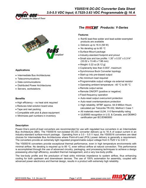
YS05S16 DC-DC Converter Data Sheet - Power-One
YS05S16 DC-DC Converter Data Sheet - Power-One
YS05S16 DC-DC Converter Data Sheet - Power-One

Create successful ePaper yourself
Turn your PDF publications into a flip-book with our unique Google optimized e-Paper software.
<strong>YS05S16</strong> <strong>DC</strong>-<strong>DC</strong> <strong>Converter</strong> <strong>Data</strong> <strong>Sheet</strong>3.0-5.5 V<strong>DC</strong> Input; 0.7525-3.63 V<strong>DC</strong> Programmable @ 16 ATheProducts: Y-SeriesApplications Intermediate Bus Architectures Telecommunications <strong>Data</strong> communications Distributed <strong>Power</strong> Architectures Servers, workstationsBenefits High efficiency – no heat sink required Reduces total solution board area Tape and reel packing Compatible with pick & place equipment Minimizes part numbers in inventoryFeatures RoHS lead-free solder and lead-solder-exemptedproducts are available Delivers up to 16 A (58 W) No derating up to 85 C Surface-Mount package Industry-standard footprint and pinout Small size and low profile: 1.30” x 0.53” x 0.314”(33.02 x 13.46 x 7.98 mm) Weight: 0.22 oz [6.12 g] Coplanarity less than 0.003”, maximum Synchronous Buck <strong>Converter</strong> topology Start-up into pre-biased output No minimum load required Programmable output voltage via external resistor Operating ambient temperature: -40 °C to 85 °C Remote output sense Remote ON/OFF (positive or negative) Fixed-frequency operation Auto-reset output overcurrent protection Auto-reset overtemperature protection High reliability, MTBF approx. 64.9 Million Hourscalculated per Telcordia TR-332, Method I Case 1 All materials meet UL94, V-0 flammability rating UL60950 recognition in U.S. & Canada, and DEMKOcertification per IEC/EN60950Description<strong>Power</strong>-<strong>One</strong>’s point-of-load converters are recommended for use with regulated bus converters in an IntermediateBus Architecture (IBA). The <strong>YS05S16</strong> non-isolated <strong>DC</strong>-<strong>DC</strong> converter delivers up to 16 A of output current in anindustry-standard surface-mount package. Operating from a 3.0 – 5.5 V input, the <strong>YS05S16</strong> converters are idealchoices for Intermediate Bus Architectures where Point-of-Load (POL) power delivery is generally a requirement.The converters provide an extremely tight regulated programmable output voltage from 0.7525 V to 3.63 V.The <strong>YS05S16</strong> converters provide exceptional thermal performance, even in high temperature environments withminimal airflow. No derating is required up to 85 C, even without airflow at natural convection. This performanceis accomplished through the use of advanced circuitry, packaging, and processing techniques to achieve a designpossessing ultra-high efficiency, excellent thermal management, and a very low-body profile.The low-body profile and the preclusion of heat sinks minimize impedance to system airflow, thus enhancingcooling for both upstream and downstream devices. The use of 100% automation for assembly, coupled withadvanced power electronics and thermal design, results in a product with extremely high reliability.MCD10205 Rev. 1.0, 24-Jun-10 Page 1 of 25 www.power-one.com
<strong>YS05S16</strong> <strong>DC</strong>-<strong>DC</strong> <strong>Converter</strong> <strong>Data</strong> <strong>Sheet</strong>3.0-5.5 V<strong>DC</strong> Input; 0.7525-3.63 V<strong>DC</strong> Programmable @ 16 AElectrical SpecificationsConditions: T A = 25 ºC, Airflow = 300 LFM (1.5 m/s), Vin = 5 V<strong>DC</strong>, Vout = 0.7525 – 3.63 V, unless otherwise specified.Absolute Maximum RatingsParameter Notes Min Typ Max UnitsInput Voltage Continuous -0.3 6 V<strong>DC</strong>Operating Ambient Temperature -40 85 °CStorage Temperature -55 125 °CFeature CharacteristicsSwitching Frequency Full Temperature Range 250 300 350 kHzOutput Voltage Trim Range 1 By external resistor, See Trim Table 1 0.7525 3.63 V<strong>DC</strong>Remote Sense Compensation 1 Percent of V OUT (NOM) 0.5 V<strong>DC</strong>Turn-On Delay Time 2Full resistive loadWith Vin = (<strong>Converter</strong> Enabled, thenVin applied) From Vin = Vin(min) to Vo = 0.1* Vo(nom) 3 3.5 4.5 msWith Enable (Vin = Vin(nom)applied, then enabled) From enable to Vo = 0.1*Vo(nom) 3 3.5 4.5 msRise time 2 From 0.1*Vo(nom) to 0.9*Vo(nom) 3 3.5 5 msON/OFF Control (Positive Logic) 3<strong>Converter</strong> Off -5 0.8 V<strong>DC</strong><strong>Converter</strong> On 2.4 5.5 V<strong>DC</strong>ON/OFF Control (Negative Logic) 3<strong>Converter</strong> Off 2.4 5.5 V<strong>DC</strong><strong>Converter</strong> On -5 0.8 V<strong>DC</strong>Additional Notes:1The output voltage should not exceed 3.63 V (taking into account both the programming and remote sense compensation).2Note that startup time is the sum of turn-on delay time and rise time.3The converter is on if ON/OFF pin is left open.4Trim resistor connected across the GND (pin 5) and TRIM (pin 3) pins of the converter.5See waveforms for dynamic response and settling time for different output voltages.MCD10205 Rev. 1.0, 24-Jun-10 Page 2 of 25 www.power-one.com
<strong>YS05S16</strong> <strong>DC</strong>-<strong>DC</strong> <strong>Converter</strong> <strong>Data</strong> <strong>Sheet</strong>3.0-5.5 V<strong>DC</strong> Input; 0.7525-3.63 V<strong>DC</strong> Programmable @ 16 AElectrical Specifications (continued)Conditions: T A = 25 ºC, Airflow = 300 LFM (1.5 m/s), Vin = 5 V<strong>DC</strong>, Vout = 0.7525 – 3.63 V, unless otherwise specified.Input CharacteristicsParameter Notes Min Typ Max UnitsOperating Input Voltage Range 3.0 5.0 5.5 V<strong>DC</strong>Input Undervoltage LockoutTurn-on Threshold Guaranteed by controller 1.95 2.05 2.15 V<strong>DC</strong>Turn-off Threshold Guaranteed by controller 1.73 1.9 2.07 V<strong>DC</strong>Maximum Input CurrentV IN = 4.5 V<strong>DC</strong>, I OUT = 16 A V OUT = 3.3 V<strong>DC</strong> 12.7 A<strong>DC</strong>V IN = 3.0 V<strong>DC</strong>, I OUT = 16 A V OUT = 2.5 V<strong>DC</strong> 15.2 A<strong>DC</strong>V IN = 3.0 V<strong>DC</strong>, I OUT = 16 A V OUT = 2.0 V<strong>DC</strong> 12.4 A<strong>DC</strong>V IN = 3.0 V<strong>DC</strong>, I OUT = 16 A V OUT = 1.8 V<strong>DC</strong> 11.3 A<strong>DC</strong>V IN = 3.0 V<strong>DC</strong>, I OUT = 16 A V OUT = 1.5 V<strong>DC</strong> 9.7 A<strong>DC</strong>V IN = 3.0 V<strong>DC</strong>, I OUT = 16 A V OUT = 1.2 V<strong>DC</strong> 8.1 A<strong>DC</strong>V IN = 3.0 V<strong>DC</strong>, I OUT = 16 A V OUT = 1.0 V<strong>DC</strong> 7.0 A<strong>DC</strong>V IN = 3.0 V<strong>DC</strong>, I OUT = 16 A V OUT = 0.7525 V<strong>DC</strong> 5.7 A<strong>DC</strong>Input Stand-by Current (<strong>Converter</strong> disabled) Vin = 5.0 V<strong>DC</strong> 3.5 mAInput No Load Current (<strong>Converter</strong> enabled) Vin = 5.5 V<strong>DC</strong>V OUT = 3.3 V<strong>DC</strong> 91 mAV OUT = 2.5 V<strong>DC</strong> 91 mAV OUT = 2.0 V<strong>DC</strong> 87 mAV OUT = 1.8 V<strong>DC</strong> 86 mAV OUT = 1.5 V<strong>DC</strong> 85 mAV OUT = 1.2 V<strong>DC</strong> 76 mAV OUT = 1.0 V<strong>DC</strong> 76 mAV OUT = 0.7525 V<strong>DC</strong> 61 mAInput Reflected-Ripple Current - i s See Fig. G for setup (BW = 20 MHz) 20 mA P-PMCD10205 Rev. 1.0, 24-Jun-10 Page 3 of 25 www.power-one.com
<strong>YS05S16</strong> <strong>DC</strong>-<strong>DC</strong> <strong>Converter</strong> <strong>Data</strong> <strong>Sheet</strong>3.0-5.5 V<strong>DC</strong> Input; 0.7525-3.63 V<strong>DC</strong> Programmable @ 16 AElectrical Specifications (continued)Conditions: T A = 25 ºC, Airflow = 300 LFM (1.5 m/s), Vin = 5 V<strong>DC</strong>, Vout = 0.7525 – 3.63 V, unless otherwise specified.Output CharacteristicsParameter Notes Min Typ Max UnitsOutput Voltage Set Point (no load) -1.5 Vout +1.5 %VoutOutput Regulation 4Over Line Full resistive load 0.75 1 %VoutOver Load From no load to full load 0.75 1 %VoutOutput Voltage Range(Over all operating input voltage, resistive loadand temperature conditions until end of life )-3 +3 %VoutOutput Ripple and Noise – 20 MHz bandwidth Over line, load and temperature (Fig. G)Peak-to-Peak V OUT = 3.3 V<strong>DC</strong> 30 60 mV P-PPeak-to-Peak V OUT = 0.7525 V<strong>DC</strong> 10 20 mV P-PExternal Load CapacitancePlus full load (resistive)Min ESR > 1 mΩ 1,000 μFMin ESR > 10 mΩ 5,000 μFOutput Current Range 0 16 AOutput Current Limit Inception (I OUT ) 18 28 38 AOutput Short-Circuit Current (Hiccup mode) Short = 10 mΩ, continuous 2 4 8 ArmsDynamic Response50% Load current change from8 A -16 A - 8 A with di/dt = 5 A/μs Co = 100 μF tant. + 1 μF ceramic 150 5 mVSettling Time (V OUT < 10% peak deviation) 60 µsEfficiency Full load (16 A)V OUT = 3.3 V<strong>DC</strong> 93.0 %V OUT = 2.5 V<strong>DC</strong> 90.5 %V OUT = 2.0 V<strong>DC</strong> 88.5 %V OUT = 1.8 V<strong>DC</strong> 87.5 %V OUT = 1.5 V<strong>DC</strong> 86.0 %V OUT = 1.2 V<strong>DC</strong> 83.5 %V OUT = 1.0 V<strong>DC</strong> 81.5 %V OUT = 0.7525 V<strong>DC</strong> 77.5 %MCD10205 Rev. 1.0, 24-Jun-10 Page 4 of 25 www.power-one.com
<strong>YS05S16</strong> <strong>DC</strong>-<strong>DC</strong> <strong>Converter</strong> <strong>Data</strong> <strong>Sheet</strong>3.0-5.5 V<strong>DC</strong> Input; 0.7525-3.63 V<strong>DC</strong> Programmable @ 16 AOperationsInput and Output ImpedanceThe <strong>YS05S16</strong> converter should be connected via alow impedance to the <strong>DC</strong> power source. In manyapplications, the inductance associated with thedistribution from the power source to the input of theconverter can affect the stability of the converter.The use of decoupling capacitors is recommended inorder to ensure stability of the converter and reduceinput ripple voltage. Internally, the converter has44 μF (low ESR ceramics) of input capacitance.In a typical application, low - ESR tantalum or POScapacitors will be sufficient to provide adequateripple voltage filtering at the input of the converter.However, very low ESR ceramic capacitors100 - 200 μF are recommended at the input of theconverter in order to minimize the input ripplevoltage. They should be placed as close as possibleto the input pins of the converter.The <strong>YS05S16</strong> has been designed for stableoperation with or without external capacitance. LowESR ceramic capacitors placed as close as possibleto the load (minimum 100 μF) are recommended forimproved transient performance and lower outputvoltage ripple.It is important to keep low resistance and lowinductance PCB traces for connecting load to theoutput pins of the converter in order to maintain goodload regulation.Fig. A shows input voltage ripple for various outputvoltages using four 47 μF input ceramic capacitors.The same plot is shown in Fig. B with one 470 μFpolymer capacitor (6TPB470M from Sanyo) inparallel with two 47 μF ceramic capacitors at fullload.Input Voltage Ripple [mVp-p]32282420161284Vin = 3.3VVin = 5.0V00 1 2 3 4Vout [V]Fig. B: Input Voltage Ripple, C IN = 470 μF polymer + 2 x 47 μFceramic.ON/OFF (Pin 1)The ON/OFF pin is used to turn the power converteron or off remotely via a system signal. There are tworemote control options available, positive logic(standard option) and negative logic, with bothreferenced to GND. The typical connections areshown in Fig. C.To turn the converter on the ON/OFF pin should beat a logic low or left open, and to turn the converteroff the ON/OFF pin should be at a logic high orconnected to Vin. See the Electrical Specificationsfor logic high/low definitions.VinR*VinON/OFFY-Series<strong>Converter</strong>(Top View)SENSEVout24GNDTRIMRloadInput Voltage Ripple [mVp-p]20161284Vin = 3.3VVin = 5.0V00 1 2 3 4Vout [V]Fig. A: Input Voltage Ripple, CIN = 4 x 47 μF ceramic, full load.CONTROLINPUTR* is for negative logic option onlyFig. C: Circuit configuration for ON/OFF function.The positive logic version turns the converter onwhen the ON/OFF pin is at a logic high or left open,and turns the converter off when at a logic low orshorted to GND.The negative logic version turns the converter onwhen the ON/OFF pin is at logic low or left open, andturns the converter off when the ON/OFF pin is at alogic high or connected to Vin.MCD10205 Rev. 1.0, 24-Jun-10 Page 5 of 25 www.power-one.com
<strong>YS05S16</strong> <strong>DC</strong>-<strong>DC</strong> <strong>Converter</strong> <strong>Data</strong> <strong>Sheet</strong>3.0-5.5 V<strong>DC</strong> Input; 0.7525-3.63 V<strong>DC</strong> Programmable @ 16 AThe ON/OFF pin is internally pulled up to Vin forpositive logic version, and pulled down for a negativelogic version. A TTL or CMOS logic gate, opencollector(open-drain) transistor can be used to driveON/OFF pin. This device must be capable of:– sinking up to 1.2 mA at a low level voltage of 0.8 V– sourcing up to 0.25 mA at a high logic level of2.3 V - 5.5 V.When using open-collector (open-drain) transistorwith a negative logic option, add a pull-up resistor(R*) to Vin as shown in Fig. C:– 20 K, if the minimum Vin is 4.5 V– 10 K, if the minimum Vin is 3.0 V– 5 K, if the undervoltage shutdown at 2.05 - 2.15 Vis required.Remote Sense (Pin 2)The remote sense feature of the convertercompensates for voltage drops occurring onlybetween Vout pin (Pin 4) of the converter and theload. The SENSE (Pin 2) pin should be connected atthe load or at the point where regulation is required(see Fig. D). There is no sense feature on the outputGND return pin, where the solid ground plane shouldprovide a low voltage drop.equal to the product of the nominal output voltageand the allowable output current for the givenconditions.When using remote sense, the output voltage at theconverter can be increased up to 0.5 V above thenominal rating in order to maintain the requiredvoltage across the load. Therefore, the designermust, if necessary, decrease the maximum current(originally obtained from the derating curves) by thesame percentage to ensure the converter’s actualoutput power remains at or below the maximumallowable output power.Output Voltage Programming (Pin 3)The output voltage can be programmed from0.7525 V to 3.63 V by connecting an external resistorbetween TRIM pin (Pin 3) and GND pin (Pin 5); seeFig. E. Note that when a trim resistor is notconnected, the output voltage of the converter is0.7525 V.VinVinON/OFFGNDY-Series<strong>Converter</strong>(Top View)SENSEVoutTRIMRloadRTRIMVinVinON/OFFGNDY-Series<strong>Converter</strong>(Top View)SENSEVoutTRIMFig. D: Remote sense circuit configuration.RwRwRloadIf remote sensing is not required, the SENSE pinmust be connected to the Vout pin (Pin 4) to ensurethe converter will regulate at the specified outputvoltage. If these connections are not made, theconverter will deliver an output voltage that is slightlyhigher than the specified value.Because the sense lead carries minimal current,large trace on the end-user board are not required.However, sense trace should be located close to aground plane to minimize system noise and ensureoptimum performance.When utilizing the remote sense feature, care mustbe taken not to exceed the maximum allowableoutput power capability of the converter, which isFig. E: Configuration for programming output voltage.A trim resistor, R TRIM , for a desired output voltagecan be calculated using the following equation:21.07RTRIM 5.11[kΩ](VO-REQ- 0.7525)where,RTRIM Required value of trim resistor [kΩ]VOREQ Desired (trimmed) output voltage [V]Note that the tolerance of a trim resistor directlyaffects the output voltage tolerance. It isrecommended to use standard 1% or 0.5% resistors;for tighter tolerance, two resistors in parallel arerecommended rather than one standard value fromTable 1.Ground pin of the trim resistor should be connecteddirectly to the converter GND pin (Pin 5) with novoltage drop in between. Table 1 provides the trimresistor values for popular output voltages.MCD10205 Rev. 1.0, 24-Jun-10 Page 6 of 25 www.power-one.com
<strong>YS05S16</strong> <strong>DC</strong>-<strong>DC</strong> <strong>Converter</strong> <strong>Data</strong> <strong>Sheet</strong>3.0-5.5 V<strong>DC</strong> Input; 0.7525-3.63 V<strong>DC</strong> Programmable @ 16 ATable 1: Trim Resistor ValueV 0-REG [V] R TRIM [kΩ]The ClosestStandard Value [kΩ]0.7525 open1.0 80.0 80.61.2 41.97 42.21.5 23.1 23.21.8 15 152.0 11.78 11.82.5 6.95 6.983.3 3.16 3.163.63 2.21 2.21The output voltage can also be programmed byexternal voltage source. To make trimming lesssensitive, a series external resistor Rext isrecommended between TRIM pin and programmingvoltage source. Control Voltage can be calculated bythe formula:(5.11REXT)(VO-REQ- 0.7525)VCTRL 0.7 [V]30.1where,VCTRL Control voltage [V]REXT External resistor between TRIM pin andvoltage source; the value can be chosen dependingon the required output voltage range [kΩ].Control voltages withshown in Table 2.REXT 0 and REXT 15K areTable 2: Control Voltage [V<strong>DC</strong>]V 0-REG [V] V CTRL (R EXT = 0) V CTRL (R EXT = 15K)0.7525 0.700 0.7001.0 0.658 0.5351.2 0.624 0.4011.5 0.573 0.2011.8 0.522 -0.0002.0 0.488 -0.1332.5 0.403 -0.4683.3 0.268 -1.0023.63 0.257 -1.044Protection FeaturesInput Undervoltage LockoutInput undervoltage lockout is standard with thisconverter. The converter will shut down when theinput voltage drops below a pre-determined voltage;it will start automatically when Vin returns to aspecified range.The input voltage must be typically 2.05 V for theconverter to turn on. Once the converter has beenturned on, it will shut off when the input voltagedrops below typically 1.9 V.Output Overcurrent Protection (OCP)The converter is protected against overcurrent andshort circuit conditions. Upon sensing an overcurrentcondition, the converter will enter hiccup mode. Onceover-load or short circuit condition is removed, Voutwill return to nominal value.Overtemperature Protection (OTP)The converter will shut down under anovertemperature condition to protect itself fromoverheating caused by operation outside the thermalderating curves, or operation in abnormal conditionssuch as system fan failure. After the converter hascooled to a safe operating temperature, it willautomatically restart.Safety RequirementsThe converter meets North American andInternational safety regulatory requirements perUL60950 and EN60950. The maximum <strong>DC</strong> voltagebetween any two pins is Vin under all operatingconditions. Therefore, the unit has ELV (extra lowvoltage) output; it meets SELV requirements underthe condition that all input voltages are ELV.The converter is not internally fused. To comply withsafety agencies’ requirements, a recognized fusewith a maximum rating of 20 Amps must be used inseries with the input line.CharacterizationGeneral InformationThe converter has been characterized for manyoperational aspects, to include thermal derating(maximum load current as a function of ambienttemperature and airflow) for vertical and horizontalmountings, efficiency, startup and shutdownparameters, output ripple and noise, transientresponse to load step-change, overload, and shortcircuit.MCD10205 Rev. 1.0, 24-Jun-10 Page 7 of 25 www.power-one.com
<strong>YS05S16</strong> <strong>DC</strong>-<strong>DC</strong> <strong>Converter</strong> <strong>Data</strong> <strong>Sheet</strong>3.0-5.5 V<strong>DC</strong> Input; 0.7525-3.63 V<strong>DC</strong> Programmable @ 16 AThe figures are numbered as Fig. x.y, where xindicates the different output voltages, and yassociates with specific plots (y = 1 for the verticalthermal derating, …). For example, Fig. x.1 will referto the vertical thermal derating for all the outputvoltages in general.The following pages contain specific plots orwaveforms associated with the converter. Additionalcomments for specific data are provided below.Test ConditionsAll data presented were taken with the convertersoldered to a test board, specifically a 0.060” thickprinted wiring board (PWB) with four layers. The topand bottom layers were not metalized. The two innerlayers, comprised of two-ounce copper, were used toprovide traces for connectivity to the converter.The lack of metalization on the outer layers as wellas the limited thermal connection ensured that heattransfer from the converter to the PWB wasminimized. This provides a worst-case but consistentscenario for thermal derating purposes.All measurements requiring airflow were made in thevertical and horizontal wind tunnels using Infrared(IR) thermography and thermocouples forthermometry.Ensuring components on the converter do notexceed their ratings is important to maintaining highreliability. If one anticipates operating the converterat or close to the maximum loads specified in thederating curves, it is prudent to check actualoperating temperatures in the application.Thermographic imaging is preferable; if thiscapability is not available, then thermocouples maybe used. . The use of AWG #40 gauge thermocoupleis recommended to ensure measurement accuracy.Careful routing of the thermocouple leads will furtherminimize measurement error. Refer to Fig. F for theoptimum measuring thermocouple location.temperature was varied between 25 °C and 85 °C,with airflow rates from 30 to 500 LFM (0.15 m/s to2.5 m/s), and vertical and horizontal mountings. Theairflow during the testing is parallel to the short axisof the converter, going from pin 1 and pin 6 topins 2–5.For each set of conditions, the maximum loadcurrent is defined as the lowest of:(i) The output current at which any MOSFETtemperature does not exceed a maximum specifiedtemperature (120°C) as indicated by thethermographic image, or(ii) The maximum current rating of the converter(16 A).During normal operation, derating curves withmaximum FET temperature less than or equal to120 °C should not be exceeded. Temperature on thePCB at the thermocouple location shown in Fig. Fshould not exceed 120 °C in order to operate insidethe derating curves.EfficiencyFig. x.3 shows the efficiency vs. load current plot forambient temperature of 25 ºC, airflow rate of200 LFM (1 m/s) and input voltages of 4.5 V, 5.0 Vand 5.5 V. Fig. x.4 is for input voltages of 3.0 V,3.3 V and 3.6 V and output voltages ≤ 2.5 V.<strong>Power</strong> DissipationFig. 3.3V.4 shows the power dissipation vs. loadcurrent plot for Ta = 25 ºC, airflow rate of 200 LFM(1 m/s) with vertical mounting and input voltages of4.5 V, 5.0 V and 5.5 V for 3.3 V output.Ripple and NoiseThe output voltage ripple waveform is measured atfull rated load current. Note that all output voltagewaveforms are measured across a 1 μF ceramiccapacitor.The output voltage ripple and input reflected-ripplecurrent waveforms are obtained using the test setupshown in Fig. G.i SFig. F: Location of the thermocouple for thermal testing.Thermal DeratingLoad current vs. ambient temperature and airflowrates are given in Figs. x.1 and Figs. x.2 formaximum temperature of 120°C. Ambient1 HsourceinductanceVsourceCIN4x47FceramiccapacitorY-Series<strong>DC</strong>-<strong>DC</strong><strong>Converter</strong>1FceramiccapacitorCO100FceramiccapacitorVoutFig. G: Test setup for measuring input reflected-ripple currents, i sand output voltage ripple.MCD10205 Rev. 1.0, 24-Jun-10 Page 8 of 25 www.power-one.com
<strong>YS05S16</strong> <strong>DC</strong>-<strong>DC</strong> <strong>Converter</strong> <strong>Data</strong> <strong>Sheet</strong>3.0-5.5 V<strong>DC</strong> Input; 0.7525-3.63 V<strong>DC</strong> Programmable @ 16 A20201616Load Current [Adc]1284500 LFM (2.5 m/s)400 LFM (2.0 m/s)300 LFM (1.5 m/s)200 LFM (1.0 m/s)100 LFM (0.5 m/s)30 LFM (0.15 m/s)Load Current [Adc]1284500 LFM (2.5 m/s)400 LFM (2.0 m/s)300 LFM (1.5 m/s)200 LFM (1.0 m/s)100 LFM (0.5 m/s)30 LFM (0.15 m/s)020 30 40 50 60 70 80 90Ambient Temperature [°C]Fig. 3.3V.1: Available load current vs. ambient temperature andairflow rates for Vout = 3.3 V converter mounted vertically with Vin= 5 V, and maximum MOSFET temperature 120 C.020 30 40 50 60 70 80 90Ambient Temperature [°C]Fig. 3.3V.2: Available load current vs. ambient temperature andairflow rates for Vout = 3.3 V converter mounted horizontally withVin = 5 V, and maximum MOSFET temperature 120 C.1.0050.954Efficiency0.900.850.805.5 V5.0 V4.5 V<strong>Power</strong> Dissipation [W]3215.5 V5.0 V4.5 V0.750 3 6 9 12 15 18Load Current [Adc]Fig. 3.3V.3: Efficiency vs. load current and input voltage for Vout= 3.3 V converter mounted vertically with air flowing at a rate of200 LFM (1 m/s) and Ta = 25 C.00 3 6 9 12 15 18Load Current [Adc]Fig. 3.3V.4: <strong>Power</strong> loss vs. load current and input voltage for Vout= 3.3 V converter mounted vertically with air flowing at a rate of200 LFM (1 m/s) and Ta = 25 C.MCD10205 Rev. 1.0, 24-Jun-10 Page 9 of 25 www.power-one.com
<strong>YS05S16</strong> <strong>DC</strong>-<strong>DC</strong> <strong>Converter</strong> <strong>Data</strong> <strong>Sheet</strong>3.0-5.5 V<strong>DC</strong> Input; 0.7525-3.63 V<strong>DC</strong> Programmable @ 16 AFig. 3.3V.5: Turn-on transient for Vout = 3.3 V with application ofVin at full rated load current (resistive) and 100 μF externalcapacitance at Vin = 5 V. Top trace: Vin (5 V/div.); Bottom trace:output voltage (1 V/div.); Time scale: 2 ms/div.Fig. 3.3V.6: Output voltage ripple (20 mV/div.) at full rated loadcurrent into a resistive load with external capacitance 100 μFceramic + 1 μF ceramic and Vin = 5 V for Vout = 3.3 V. Timescale: 2 μs/div.Fig. 3.3V.7: Output voltage for Vout = 3.3 V to positive loadcurrent step change from 8 A to 16 A with slew rate of 5 A/μs atVin = 5 V. Top trace: output voltage (100 mV/div.); Bottom trace:load current (5 A/div.). Co = 100 μF ceramic. Time scale: 20μs/div.Fig. 3.3V.8: Output voltage response for Vout = 3.3 V to negativeload current step change from 16 A to 8 A with slew rate of -5 A/μsat Vin = 5 V. Top trace: output voltage (100 mV/div.); Bottomtrace: load current (5 A/div.). Co = 100 μF ceramic. Time scale:20 μs/div.MCD10205 Rev. 1.0, 24-Jun-10 Page 10 of 25 www.power-one.com
<strong>YS05S16</strong> <strong>DC</strong>-<strong>DC</strong> <strong>Converter</strong> <strong>Data</strong> <strong>Sheet</strong>3.0-5.5 V<strong>DC</strong> Input; 0.7525-3.63 V<strong>DC</strong> Programmable @ 16 A20201616Load Current [Adc]1284500 LFM (2.5 m/s)400 LFM (2.0 m/s)300 LFM (1.5 m/s)200 LFM (1.0 m/s)100 LFM (0.5 m/s)30 LFM (0.15 m/s)Load Current [Adc]1284500 LFM (2.5 m/s)400 LFM (2.0 m/s)300 LFM (1.5 m/s)200 LFM (1.0 m/s)100 LFM (0.5 m/s)30 LFM (0.15 m/s)020 30 40 50 60 70 80 90Ambient Temperature [°C]Fig. 2.5V.1: Available load current vs. ambient temperature andairflow rates for Vout = 2.5 V converter mounted vertically with Vin= 5 V, and maximum MOSFET temperature 120 C.020 30 40 50 60 70 80 90Ambient Temperature [°C]Fig. 2.5V.2: Available load current vs. ambient temperature andairflow rates for Vout = 2.5 V converter mounted horizontally withVin = 5 V, and maximum MOSFET temperature 120 C.1.001.000.950.95Efficiency0.900.85Efficiency0.900.850.805.5 V5.0 V4.5 V0.803.6 V3.3 V3.0 V0.750 3 6 9 12 15 18Load Current [Adc]Fig. 2.5V.3: Efficiency vs. load current and input voltage for Vout= 2.5 V converter mounted vertically with air flowing at a rate of200 LFM (1 m/s) and Ta = 25 C.0.750 3 6 9 12 15 18Load Current [Adc]Fig. 2.5V.4: Efficiency vs. load current and input voltage for Vout= 2.5 V converter mounted vertically with air flowing at a rate of200 LFM (1 m/s) and Ta = 25 C.MCD10205 Rev. 1.0, 24-Jun-10 Page 11 of 25 www.power-one.com
<strong>YS05S16</strong> <strong>DC</strong>-<strong>DC</strong> <strong>Converter</strong> <strong>Data</strong> <strong>Sheet</strong>3.0-5.5 V<strong>DC</strong> Input; 0.7525-3.63 V<strong>DC</strong> Programmable @ 16 AFig. 2.5V.5: Turn-on transient for Vout = 2.5 V with application ofVin at full rated load current (resistive) and 100 μF externalcapacitance at Vin = 5 V. Top trace: Vin (5 V/div.); Bottom trace:output voltage (1 V/div.); Time scale: 2 ms/div.Fig. 2.5V.6: Output voltage ripple (20 mV/div.) at full rated loadcurrent into a resistive load with external capacitance 100 μFceramic + 1 μF ceramic and Vin = 5 V for Vout = 2.5 V. Timescale: 2 μs/div.Fig. 2.5V.7: Output voltage response for Vout = 2.5 V to positiveload current step change from 8 A to 16 A with slew rate of 5 A/μsat Vin = 5 V. Top trace: output voltage (100 mV/div.); Bottomtrace: load current (5 A/div.). Co = 100 μF ceramic. Time scale:20 μs/div.Fig. 2.5V.8: Output voltage response for Vout = 2.5 V to negativeload current step change from 16 A to 8 A with slew rate of -5 A/μsat Vin = 5 V. Top trace: output voltage (100 mV/div.); Bottomtrace: load current (5 A/div.). Co = 100 μF ceramic. Time scale:20 μs/div.MCD10205 Rev. 1.0, 24-Jun-10 Page 12 of 25 www.power-one.com
<strong>YS05S16</strong> <strong>DC</strong>-<strong>DC</strong> <strong>Converter</strong> <strong>Data</strong> <strong>Sheet</strong>3.0-5.5 V<strong>DC</strong> Input; 0.7525-3.63 V<strong>DC</strong> Programmable @ 16 A20201616Load Current [Adc]1284500 LFM (2.5 m/s)400 LFM (2.0 m/s)300 LFM (1.5 m/s)200 LFM (1.0 m/s)100 LFM (0.5 m/s)30 LFM (0.15 m/s)Load Current [Adc]1284500 LFM (2.5 m/s)400 LFM (2.0 m/s)300 LFM (1.5 m/s)200 LFM (1.0 m/s)100 LFM (0.5 m/s)30 LFM (0.15 m/s)020 30 40 50 60 70 80 90Ambient Temperature [°C]Fig. 2.0V.1: Available load current vs. ambient temperature andairflow rates for Vout = 2.0 V converter mounted vertically with Vin= 5 V, and maximum MOSFET temperature 120 C.020 30 40 50 60 70 80 90Ambient Temperature [°C]Fig. 2.0V.2: Available load current vs. ambient temperature andairflow rates for Vout = 2.0 V converter mounted horizontally withVin = 5 V, and maximum MOSFET temperature 120 C.0.950.950.900.90Efficiency0.850.80Efficiency0.850.800.755.5 V5.0 V4.5 V0.753.6 V3.3 V3.0 V0.700 3 6 9 12 15 18Load Current [Adc]Fig. 2.0V.3: Efficiency vs. load current and input voltage for Vout= 2.0 V converter mounted vertically with air flowing at a rate of200 LFM (1 m/s) and Ta = 25 C.0.700 3 6 9 12 15 18Load Current [Adc]Fig. 2.0V.4: Efficiency vs. load current and input voltage for Vout= 2.0 V converter mounted vertically with air flowing at a rate of200 LFM (1 m/s) and Ta = 25 C.MCD10205 Rev. 1.0, 24-Jun-10 Page 13 of 25 www.power-one.com
<strong>YS05S16</strong> <strong>DC</strong>-<strong>DC</strong> <strong>Converter</strong> <strong>Data</strong> <strong>Sheet</strong>3.0-5.5 V<strong>DC</strong> Input; 0.7525-3.63 V<strong>DC</strong> Programmable @ 16 AFig. 2.0V.5: Turn-on transient for Vout = 2.0 V with application ofVin at full rated load current (resistive) and 100μF externalcapacitance at Vin = 5 V. Top trace: Vin (5 V/div.); Bottom trace:output voltage (1 V/div.); Time scale: 2 ms/div.Fig. 2.0V.6: Output voltage ripple (20 mV/div.) at full rated loadcurrent into a resistive load with external capacitance 100 μFceramic + 1 μF ceramic and Vin = 5 V for Vout = 2.0 V. Timescale: 2 μs/div.Fig. 2.0V.7: Output voltage response for Vout = 2.0 V to positiveload current step change from 8 A to 16 A with slew rate of 5 A/μsat Vin = 5 V. Top trace: output voltage (100 mV/div.); Bottomtrace: load current (5 A/div.). Co = 100 μF ceramic. Time scale:20 μs/div.Fig. 2.0V.8: Output voltage response for Vout = 2.0V to negative load current step change from 16 A to8 A with slew rate of -5 A/μs at Vin = 5 V. Top trace:output voltage (100 mV/div.); Bottom trace: loadcurrent (5 A/div.). Co = 100 μF ceramic. Time scale:20 μs/div.MCD10205 Rev. 1.0, 24-Jun-10 Page 14 of 25 www.power-one.com
<strong>YS05S16</strong> <strong>DC</strong>-<strong>DC</strong> <strong>Converter</strong> <strong>Data</strong> <strong>Sheet</strong>3.0-5.5 V<strong>DC</strong> Input; 0.7525-3.63 V<strong>DC</strong> Programmable @ 16 A20201616Load Current [Adc]1284500 LFM (2.5 m/s)400 LFM (2.0 m/s)300 LFM (1.5 m/s)200 LFM (1.0 m/s)100 LFM (0.5 m/s)30 LFM (0.15 m/s)Load Current [Adc]1284500 LFM (2.5 m/s)400 LFM (2.0 m/s)300 LFM (1.5 m/s)200 LFM (1.0 m/s)100 LFM (0.5 m/s)30 LFM (0.15 m/s)020 30 40 50 60 70 80 90Ambient Temperature [°C]020 30 40 50 60 70 80 90Ambient Temperature [°C]Fig. 1.8V.1: Available load current vs. ambient temperature andairflow rates for Vout = 1.8 V converter mounted vertically with Vin= 5 V, and maximum MOSFET temperature 120 C.Fig. 1.8V.2: Available load current vs. ambient temperature andairflow rates for Vout = 1.8 V converter mounted horizontally withVin = 5 V, and maximum MOSFET temperature 120 C.0.950.950.900.90Efficiency0.850.80Efficiency0.850.800.755.5 V5.0 V4.5 V0.753.6 V3.3 V3.0 V0.700 3 6 9 12 15 18Load Current [Adc]Fig. 1.8V.3: Efficiency vs. load current and input voltage for Vout= 1.8 V converter mounted vertically with air flowing at a rate of200 LFM (1 m/s) and Ta = 25 C.0.700 3 6 9 12 15 18Load Current [Adc]Fig. 1.8V.4: Efficiency vs. load current and input voltage for Vout= 1.8 V converter mounted vertically with air flowing at a rate of200 LFM (1 m/s) and Ta = 25 C.MCD10205 Rev. 1.0, 24-Jun-10 Page 15 of 25 www.power-one.com
<strong>YS05S16</strong> <strong>DC</strong>-<strong>DC</strong> <strong>Converter</strong> <strong>Data</strong> <strong>Sheet</strong>3.0-5.5 V<strong>DC</strong> Input; 0.7525-3.63 V<strong>DC</strong> Programmable @ 16 AFig. 1.8V.5: Turn-on transient for Vout = 1.8 V with application ofVin at full rated load current (resistive) and 100μF externalcapacitance at Vin = 5 V. Top trace: Vin (5 V/div.); Bottom trace:output voltage (1V/div.); Time scale: 2 ms/div.Fig. 1.8V.6: Output voltage ripple (20 mV/div.) at full rated loadcurrent into a resistive load with external capacitance 100 μFceramic + 1 μF ceramic and Vin = 5 V for Vout = 1.8 V. Timescale: 2 μs/div.Fig. 1.8V.7: Output voltage response for Vout = 1.8 V to positiveload current step change from 8 A to 16 A with slew rate of 5 A/μsat Vin = 5 V. Top trace: output voltage (100 mV/div.); Bottomtrace: load current (5 A/div.). Co = 100 μF ceramic. Time scale:20 μs/div.Fig. 1.8V.8: Output voltage response for Vout = 1.8 V to negativeload current step change from 16 A to 8 A with slew rate of -5 A/μsat Vin = 5 V. Top trace: output voltage (100 mV/div.); Bottomtrace: load current (5 A/div.). Co = 100 μF ceramic. Time scale:20 μs/div.MCD10205 Rev. 1.0, 24-Jun-10 Page 16 of 25 www.power-one.com
<strong>YS05S16</strong> <strong>DC</strong>-<strong>DC</strong> <strong>Converter</strong> <strong>Data</strong> <strong>Sheet</strong>3.0-5.5 V<strong>DC</strong> Input; 0.7525-3.63 V<strong>DC</strong> Programmable @ 16 A20201616Load Current [Adc]1284500 LFM (2.5 m/s)400 LFM (2.0 m/s)300 LFM (1.5 m/s)200 LFM (1.0 m/s)100 LFM (0.5 m/s)30 LFM (0.15 m/s)Load Current [Adc]1284500 LFM (2.5 m/s)400 LFM (2.0 m/s)300 LFM (1.5 m/s)200 LFM (1.0 m/s)100 LFM (0.5 m/s)30 LFM (0.15 m/s)020 30 40 50 60 70 80 90Ambient Temperature [°C]Fig. 1.5V.1: Available load current vs. ambient temperature andairflow rates for Vout = 1.5 V converter mounted vertically with Vin= 5 V, and maximum MOSFET temperature 120 C.020 30 40 50 60 70 80 90Ambient Temperature [°C]Fig. 1.5V.2: Available load current vs. ambient temperature andairflow rates for Vout = 1.5 V converter mounted horizontally withVin = 5 V, and maximum MOSFET temperature 120 C.0.950.950.900.90Efficiency0.850.80Efficiency0.850.800.755.5 V5.0 V4.5 V0.753.6 V3.3 V3.0 V0.700 3 6 9 12 15 18Load Current [Adc]Fig. 1.5V.3: Efficiency vs. load current and input voltage for Vout= 1.5 V converter mounted vertically with air flowing at a rate of200 LFM (1 m/s) and Ta = 25 C.0.700 3 6 9 12 15 18Load Current [Adc]Fig. 1.5V.4: Efficiency vs. load current and input voltage for Vout= 1.5 V converter mounted vertically with air flowing at a rate of200 LFM (1 m/s) and Ta = 25 C.MCD10205 Rev. 1.0, 24-Jun-10 Page 17 of 25 www.power-one.com
<strong>YS05S16</strong> <strong>DC</strong>-<strong>DC</strong> <strong>Converter</strong> <strong>Data</strong> <strong>Sheet</strong>3.0-5.5 V<strong>DC</strong> Input; 0.7525-3.63 V<strong>DC</strong> Programmable @ 16 AFig. 1.5V.5: Turn-on transient for Vout = 1.5 V with application ofVin at full rated load current (resistive) and 100 μF externalcapacitance at Vin = 5 V. Top trace: Vin (5 V/div.); Bottom trace:output voltage (1 V/div.); Time scale: 2 ms/div.Fig. 1.5V.6: Output voltage ripple (20 mV/div.) at full rated loadcurrent into a resistive load with external capacitance 100 μFceramic + 1 μF ceramic and Vin = 5 V for Vout = 1.5 V. Timescale: 2 μs/div.Fig. 1.5V.7: Output voltage response for Vout = 1.5 V to positiveload current step change from 8 A to 16 A with slew rate of 5 A/μsat Vin = 5V. Top trace: output voltage (100 mV/div.); Bottom trace:load current (5 A/div.). Co = 100 μF ceramic. Time scale:20 μs/div.Fig. 1.5V.8: Output voltage response for Vout = 1.5 V to negativeload current step change from 16 A to 8 A with slew rate of -5 A/μsat Vin = 5 V. Top trace: output voltage (100 mV/div.); Bottomtrace: load current (5 A/div.). Co = 100 μF ceramic. Time scale:20 μs/div.MCD10205 Rev. 1.0, 24-Jun-10 Page 18 of 25 www.power-one.com
<strong>YS05S16</strong> <strong>DC</strong>-<strong>DC</strong> <strong>Converter</strong> <strong>Data</strong> <strong>Sheet</strong>3.0-5.5 V<strong>DC</strong> Input; 0.7525-3.63 V<strong>DC</strong> Programmable @ 16 A20201616Load Current [Adc]1284500 LFM (2.5 m/s)400 LFM (2.0 m/s)300 LFM (1.5 m/s)200 LFM (1.0 m/s)100 LFM (0.5 m/s)30 LFM (0.15 m/s)Load Current [Adc]1284500 LFM (2.5 m/s)400 LFM (2.0 m/s)300 LFM (1.5 m/s)200 LFM (1.0 m/s)100 LFM (0.5 m/s)30 LFM (0.15 m/s)020 30 40 50 60 70 80 90Ambient Temperature [°C]Fig. 1.2V.1: Available load current vs. ambient temperature andairflow rates for Vout = 1.2 V converter mounted vertically with Vin= 5 V, and maximum MOSFET temperature 120 C.020 30 40 50 60 70 80 90Ambient Temperature [°C]Fig. 1.2V.2: Available load current vs. ambient temperature andairflow rates for Vout = 1.2 V converter mounted horizontally withVin = 5 V, and maximum MOSFET temperature 120 C.0.900.900.850.85Efficiency0.800.75Efficiency0.800.750.705.5 V5.0 V4.5 V0.703.6 V3.3 V3.0 V0.650 3 6 9 12 15 18Load Current [Adc]Fig. 1.2V.3: Efficiency vs. load current and input voltage for Vout= 1.2 V converter mounted vertically with air flowing at a rate of200 LFM (1 m/s) and Ta = 25 C.0.650 3 6 9 12 15 18Load Current [Adc]Fig. 1.2V.4: Efficiency vs. load current and input voltage for Vout= 1.2 V converter mounted vertically with air flowing at a rate of200 LFM (1 m/s) and Ta = 25 C.MCD10205 Rev. 1.0, 24-Jun-10 Page 19 of 25 www.power-one.com
<strong>YS05S16</strong> <strong>DC</strong>-<strong>DC</strong> <strong>Converter</strong> <strong>Data</strong> <strong>Sheet</strong>3.0-5.5 V<strong>DC</strong> Input; 0.7525-3.63 V<strong>DC</strong> Programmable @ 16 AFig. 1.2V.5: Turn-on transient for Vout = 1.2 V with application ofVin at full rated load current (resistive) and 100 μF externalcapacitance at Vin = 5 V. Top trace: Vin (5 V/div.); Bottom trace:output voltage (1 V/div.); Time scale: 2 ms/div.Fig. 1.2V.6: Output voltage ripple (20 mV/div.) at full rated loadcurrent into a resistive load with external capacitance 100 μFceramic + 1 μF ceramic and Vin = 5 V for Vout = 1.2 V. Timescale: 2 μs/div.Fig. 1.2V.6: Output voltage response for Vout = 1.2 V to positiveload current step change from 8 A to 16 A with slew rate of 5 A/μsat Vin = 5 V. Top trace: output voltage (100 mV/div.); Bottomtrace: load current (5 A/div.). Co = 100 μF ceramic. Time scale:20 μs/div.Fig. 1.2V.8: Output voltage response for Vout = 1.2 V to negativeload current step change from 16 A to 8 A with slew rate of -5 A/μsat Vin = 5 V. Top trace: output voltage (100 mV/div.); Bottomtrace: load current (5 A/div.). Co = 100 μF ceramic. Time scale:20 μs/div.MCD10205 Rev. 1.0, 24-Jun-10 Page 20 of 25 www.power-one.com
<strong>YS05S16</strong> <strong>DC</strong>-<strong>DC</strong> <strong>Converter</strong> <strong>Data</strong> <strong>Sheet</strong>3.0-5.5 V<strong>DC</strong> Input; 0.7525-3.63 V<strong>DC</strong> Programmable @ 16 A20201616Load Current [Adc]1284500 LFM (2.5 m/s)400 LFM (2.0 m/s)300 LFM (1.5 m/s)200 LFM (1.0 m/s)100 LFM (0.5 m/s)30 LFM (0.15 m/s)Load Current [Adc]1284500 LFM (2.5 m/s)400 LFM (2.0 m/s)300 LFM (1.5 m/s)200 LFM (1.0 m/s)100 LFM (0.5 m/s)30 LFM (0.15 m/s)020 30 40 50 60 70 80 90Ambient Temperature [°C]Fig. 1.0V.1: Available load current vs. ambient temperature andairflow rates for Vout = 1.0 V converter mounted vertically with Vin= 5 V, and maximum MOSFET temperature 120 C.020 30 40 50 60 70 80 90Ambient Temperature [°C]Fig. 1.0V.2: Available load current vs. ambient temperature andairflow rates for Vout = 1.0 V converter mounted horizontally withVin = 5 V, and maximum MOSFET temperature 120 C.0.900.900.850.85Efficiency0.800.75Efficiency0.800.750.705.5 V5.0 V4.5 V0.703.6 V3.3 V3.0 V0.650 3 6 9 12 15 18Load Current [Adc]Fig. 1.0V.3: Efficiency vs. load current and input voltage for Vout= 1.0 V converter mounted vertically with air flowing at a rate of200 LFM (1 m/s) and Ta = 25 C.0.650 3 6 9 12 15 18Load Current [Adc]Fig. 1.0V.4: Efficiency vs. load current and input voltage for Vout= 1.0 V converter mounted vertically with air flowing at a rate of200 LFM (1 m/s) and Ta = 25 C.MCD10205 Rev. 1.0, 24-Jun-10 Page 21 of 25 www.power-one.com
<strong>YS05S16</strong> <strong>DC</strong>-<strong>DC</strong> <strong>Converter</strong> <strong>Data</strong> <strong>Sheet</strong>3.0-5.5 V<strong>DC</strong> Input; 0.7525-3.63 V<strong>DC</strong> Programmable @ 16 AFig. 1.0V.5: Turn-on transient for Vout = 1.0 V with application ofVin at full rated load current (resistive) and 100 μF externalcapacitance at Vin = 5 V. Top trace: Vin (5 V/div.); Bottom trace:output voltage (1 V/div.); Time scale: 2 ms/div.Fig. 1.0V.6: Output voltage ripple (20 mV/div.) at full rated loadcurrent into a resistive load with external capacitance 100 μFceramic + 1 μF ceramic and Vin = 5 V for Vout = 1.0 V. Timescale: 2 μs/div.Fig. 1.0V.7: Output voltage response Vout = 1.0 V to positive loadcurrent step change from 8 A to 16 A with slew rate of 5 A/μs atVin = 5 V. Top trace: output voltage (100 mV/div.); Bottom trace:load current (5 A/div.). Co = 100 μF ceramic + 1 μF ceramic. Timescale: 20 μs/div.Fig. 1.0V.8: Output voltage response for Vout = 1.0 V to negativeload current step change from 16 A to 8 A with slew rate of -5 A/μsat Vin = 5 V. Top trace: output voltage (100 mV/div.); Bottomtrace: load current (5 A/div.). Co = 100 μF ceramic + 1 μFceramic. Time scale: 20 μs/div.MCD10205 Rev. 1.0, 24-Jun-10 Page 22 of 25 www.power-one.com
<strong>YS05S16</strong> <strong>DC</strong>-<strong>DC</strong> <strong>Converter</strong> <strong>Data</strong> <strong>Sheet</strong>3.0-5.5 V<strong>DC</strong> Input; 0.7525-3.63 V<strong>DC</strong> Programmable @ 16 A2020Load Current [Adc]161284500 LFM (2.5 m/s)400 LFM (2.0 m/s)300 LFM (1.5 m/s)200 LFM (1.0 m/s)100 LFM (0.5 m/s)30 LFM (0.15 m/s)Load Current [Adc]161284500 LFM (2.5 m/s)400 LFM (2.0 m/s)300 LFM (1.5 m/s)200 LFM (1.0 m/s)100 LFM (0.5 m/s)30 LFM (0.15 m/s)020 30 40 50 60 70 80 90Ambient Temperature [°C]Fig. 0.7525V.1: Available load current vs. ambient temperatureand airflow rates for Vout = 0.7525 V converter mounted verticallywith Vin = 5 V, and maximum MOSFET temperature 120 C.020 30 40 50 60 70 80 90Ambient Temperature [°C]Fig. 0.7525V.2: Available load current vs. ambient temperatureand airflow rates for Vout = 0.7525 V converter mountedhorizontally with Vin = 5 V, and maximum MOSFET temperature 120 C.0.850.850.800.80Efficiency0.750.70Efficiency0.750.700.655.5 V5.0 V4.5 V0.653.6 V3.3 V3.0 V0.600 3 6 9 12 15 18Load Current [Adc]Fig. 0.7525V.3: Efficiency vs. load current and input voltage forVout = 0.7525 V converter mounted vertically with air flowing at arate of 200 LFM (1 m/s) and Ta = 25 C.0.600 3 6 9 12 15 18Load Current [Adc]Fig. 0.7525V.4: Efficiency vs. load current and input voltage forVout = 0.7525 V converter mounted vertically with air flowing at arate of 200 LFM (1 m/s) and Ta = 25 C.MCD10205 Rev. 1.0, 24-Jun-10 Page 23 of 25 www.power-one.com
<strong>YS05S16</strong> <strong>DC</strong>-<strong>DC</strong> <strong>Converter</strong> <strong>Data</strong> <strong>Sheet</strong>3.0-5.5 V<strong>DC</strong> Input; 0.7525-3.63 V<strong>DC</strong> Programmable @ 16 AFig. 0.7525V.5: Turn-on transient for Vout = 0.7525 V withapplication of Vin at full rated load current (resistive) and100 μF external capacitance at Vin = 5 V. Top trace: Vin(5 V/div.); Bottom trace: output voltage (1 V/div.); Time scale: 2ms/div.Fig. 0.7525V.6: Output voltage ripple (20 mV/div.) at full ratedload current into a resistive load with external capacitance 100 μFceramic + 1 μF ceramic and Vin = 5 V for Vout =0.7525 V. Time scale: 2 μs/div.Fig. 0.7525V.7: Output voltage response for Vout = 0.7525 V topositive load current step change from 8 A to 16 A with slew rateof 5 A/μs at Vin = 5 V. Top trace: output voltage (100 mV/div.);Bottom trace: load current (5 A/div.). Co = 100 μF ceramic. Timescale: 20 μs/div.Fig. 0.7525V.8: Output voltage response for Vout = 0.7525 V tonegative load current step change from 16 A to 8 A with slew rateof -5 A/μs at Vin = 5 V. Top trace: output voltage (100 mV/div.);Bottom trace: load current (5 A/div.). Co = 100 μF ceramic. Timescale: 20 μs/div.MCD10205 Rev. 1.0, 24-Jun-10 Page 24 of 25 www.power-one.com
<strong>YS05S16</strong> <strong>DC</strong>-<strong>DC</strong> <strong>Converter</strong> <strong>Data</strong> <strong>Sheet</strong>3.0-5.5 V<strong>DC</strong> Input; 0.7525-3.63 V<strong>DC</strong> Programmable @ 16 APhysical InformationYS05S Pinout (Surface-Mount)Pad/Pin ConnectionsPad/Pin # Function1 ON/OFF2 SENSE3 TRIM4 Vout5 GND6 Vin23 4 51(*)TOP VIEW(*) PIN # 1 ROTATED 90°SIDE VIEW6YS05S Platform Notes All dimensions are in inches [mm] Connector Material: Copper Connector Finish: Gold over Nickel <strong>Converter</strong> Weight: 0.22 oz [6.12 g] <strong>Converter</strong> Height: 0.327” Max., 0.301” Min. Recommended Surface-Mount Pads:Min. 0.080” X 0.112” [2.03 x 2.84]<strong>Converter</strong> Part Numbering SchemeProductSeriesInputVoltageMountingSchemeRated LoadCurrentEnable LogicYS 05 S 16 – 0EnvironmentalY-Series3.0 – 5.5 VS Surface-Mount16 A(0.7525 V to 3.63 V)0 Standard(Positive Logic)D Opposite ofStandard(Negative Logic)No Suffix RoHSlead-solder-exemptcompliantG RoHScompliant for all sixsubstancesThe example above describes P/N <strong>YS05S16</strong>-0: 3.0 – 5.5 V input, surface mount, 16 A at 0.7525 V to 3.63 V output, standardenable logic, and Eutectic Tin/Lead solder. Please consult factory for the complete list of available options.NUCLEAR AND MEDICAL APPLICATIONS - <strong>Power</strong>-<strong>One</strong> products are not designed, intended for use in, or authorized for use as criticalcomponents in life support systems, equipment used in hazardous environments, or nuclear control systems without the express writtenconsent of the respective divisional president of <strong>Power</strong>-<strong>One</strong>, Inc.TECHNICAL REVISIONS - The appearance of products, including safety agency certifications pictured on labels, may change depending onthe date manufactured. Specifications are subject to change without notice.MCD10205 Rev. 1.0, 24-Jun-10 Page 25 of 25 www.power-one.com