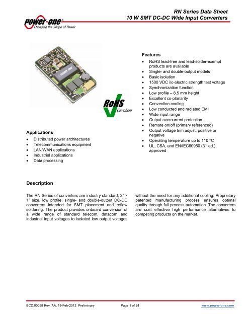
RN Series Data Sheet 10 W SMT DC-DC Wide Input ... - Power-One
RN Series Data Sheet 10 W SMT DC-DC Wide Input ... - Power-One
RN Series Data Sheet 10 W SMT DC-DC Wide Input ... - Power-One

Create successful ePaper yourself
Turn your PDF publications into a flip-book with our unique Google optimized e-Paper software.
<strong>RN</strong> <strong>Series</strong> <strong>Data</strong> <strong>Sheet</strong><strong>10</strong> W <strong>SMT</strong> <strong>DC</strong>-<strong>DC</strong> <strong>Wide</strong> <strong>Input</strong> ConvertersApplications• Distributed power architectures• Telecommunications equipment• LAN/WAN applications• Industrial applications• <strong>Data</strong> processingFeatures• RoHS lead-free and lead-solder-exemptproducts are available• Single- and double-output models• Basic isolation• 1500 V<strong>DC</strong> i/o electric strength test voltage• Synchronization function• Low profile – 8.5 mm height• Excellent co-planarity• Convection cooling• Low conducted and radiated EMI• <strong>Wide</strong> input range• Output overcurrent protection• Remote on/off (primary referenced)• Output voltage trim adjust, positive ornegative• Operating temperature up to 1<strong>10</strong> °C• UL, CSA, and EN/IEC60950 (3 rd ed.)approvedDescriptionThe <strong>RN</strong> <strong>Series</strong> of converters are industry standard, 2” ×1” size, low profile, single- and double-output <strong>DC</strong>-<strong>DC</strong>converters intended for <strong>SMT</strong> placement and reflowsoldering. The product provides onboard conversion ofa wide range of standard telecom, datacom andindustrial input voltages to isolated low output voltageswithout the need for any additional cooling. Proprietarypatented manufacturing process ensures optimalquality through full process automation. The convertersare cost effective high performance alternatives tocompeting products on the market.BCD.00038 Rev. AA, 19-Feb-2012 Preliminary Page 1 of 24 www.power-one.com
<strong>RN</strong> <strong>Series</strong> <strong>Data</strong> <strong>Sheet</strong><strong>10</strong> W <strong>SMT</strong> <strong>DC</strong>-<strong>DC</strong> <strong>Wide</strong> <strong>Input</strong> Converters.Model SelectionSingle-output modelsModel 1<strong>Input</strong>voltageV<strong>DC</strong>Max inputcurrentAOutputvoltageVOutput ratedcurrentAOutputripple/noisemV ppTypicalefficiency%<strong>RN</strong>S01EE-M6 18 – 72 0.5 3.30 1.5 25 78<strong>RN</strong>S03ZE-M6 38 – 75 0.4 2.50 2 / 3.30 3.0 50 79<strong>RN</strong>S01EG-M6 18 – 72 0.5 5.05 1.2 25 79<strong>RN</strong>S02ZG-M6 38 – 75 0.4 5.05 2.0 50 83<strong>RN</strong>S0.9ET-M6 18 – 72 0.5 7.00 0.9 25 80<strong>RN</strong>S0.6ZH-M6 38 – 75 0.3 12.0 / 15.0 2 0.6 40 831 Replace M6 by M6G for products, which comply to RoHS for all 6 substances.2 Output voltage adjusted using the trim functionDouble-output modelsModel 1<strong>Input</strong>voltageV<strong>DC</strong>Max. inputcurrentA<strong>RN</strong>D02ZGE-M6 38 – 75 0.4OutputvoltageVOutput ratedcurrentA+3.27 1.0+5.20 1.0Outputripple/noisemV ppTypicalefficiency%50 81<strong>RN</strong>D02ZGG-M6 38 – 75 0.4 ±5.<strong>10</strong> ± 1.0 50 81<strong>RN</strong>D0.8ZHH-M6 36 – 75 0.4 ±12.0 / ±15.0 2 ± 0.42 50 851 Replace M6 by M6G for products, which comply to RoHS for all 6 substances.2 Output voltage adjusted using the trim functionBCD.00038 Rev. AA, 19-Feb-2012 Preliminary Page 2 of 24 www.power-one.com
<strong>RN</strong> <strong>Series</strong> <strong>Data</strong> <strong>Sheet</strong><strong>10</strong> W <strong>SMT</strong> <strong>DC</strong>-<strong>DC</strong> <strong>Wide</strong> <strong>Input</strong> ConvertersAbsolute Maximum RatingsStresses in excess of the absolute maximum ratings may cause performance degradation, adversely affectlong-term reliability and cause permanent damage to the converter.All specifications apply over specified input voltage, output load and temperature range, unless otherwisenoted.Parameter Conditions/Description Min Max Unit<strong>Input</strong> voltage (Vin)Continuous<strong>RN</strong>S01EE/<strong>RN</strong>S01EG/<strong>RN</strong>S0.9ET (18) (72) V<strong>DC</strong>all other models38 75 V<strong>DC</strong>Transient input voltage (Vint) Transient, <strong>10</strong>0 ms <strong>10</strong>0 V<strong>DC</strong>Operating CaseTemp. (Tc) All operating conditions -45 1<strong>10</strong> °CStorage Temperature (Ts) -55 125 °CON/OFF Control Voltage (Vrc) Referenced to -Vin -5 16 VEnvironmental and Mechanical SpecificationsParameter Conditions/Description Min Nom Max UnitShock IEC68-2-27 <strong>10</strong>0 gSinusoidal Vibration IEC68-2-6 <strong>10</strong> gWeight 0.6/17 oz/gWater Washing Standard process YesMTBFPer Bellcore TR-NWT-000332(<strong>10</strong>0% load at 25 °C,GB)4590 <strong>10</strong>00 hIsolation SpecificationsParameter Conditions/Description Min Nom Max UnitInsulation Safety Rating Basic insulation --Electriic strength test voltage 1500 V<strong>DC</strong>Insulation Resistance (Rps) <strong>10</strong> MΩInsulation Capacitance (Cps) 2200 pFBCD.00038 Rev. AA, 19-Feb-2012 Preliminary Page 3 of 24 www.power-one.com
<strong>RN</strong> <strong>Series</strong> <strong>Data</strong> <strong>Sheet</strong><strong>10</strong> W <strong>SMT</strong> <strong>DC</strong>-<strong>DC</strong> <strong>Wide</strong> <strong>Input</strong> Converters<strong>RN</strong>S01EG : 5.05 V / 1.2 AAll specifications apply over input voltage, output load and temperature of 25 °C, unless otherwise noted.Parameter Conditions/Description Min Nom Max UnitsOutput VoltageVo Vin.Nom, Io = 0.2 A, 25 °C 5.02 5.05 5.08 V<strong>DC</strong>Setpoint AccuracyOutput Current * Io Vin.Min to Vin.Max 0.15 1.2 A<strong>DC</strong>Line Regulation Vin.Min to Vin.Max, 50%60 <strong>10</strong>0 mVIo.MaxLoad Regulation Vin.Nom, Io.Min to Io.Max 40 <strong>10</strong>0 mVDynamic RegulationPeak DeviationSettling Time50-<strong>10</strong>0% Io.Max load stepchange.to 1% error band250300± mVμsOutput Voltage Ripple Vr Vin.Min to Vin.Max, Io.Min to25 50 mVp-pIo Max, 20 MHz BandwidthAdmissible Load Comax Io.Max, Vin.Nom 2,200 μFCapacitanceOutput Current Limit Icl Vout ≤0.90 Vo.Nom 1<strong>10</strong> 150 %Io.MaxThresholdSwitching Frequency Fs Vin.Nom, Io.Max 4<strong>10</strong> kHzTemperatureTco 0.02 %Vo/°CCoefficientTrim Range Vt Io.Min to Io.Max, Vin.Min toVin.Max4.3 5.9 Vo* At Iout
<strong>RN</strong> <strong>Series</strong> <strong>Data</strong> <strong>Sheet</strong><strong>10</strong> W <strong>SMT</strong> <strong>DC</strong>-<strong>DC</strong> <strong>Wide</strong> <strong>Input</strong> Converters<strong>RN</strong>S02ZG : 5.05 V / 2.0 AAll specifications apply over input voltage, output load and temperature range, unless otherwise noted.Parameter Conditions/Description Min Nom Max UnitsOutput VoltageVo Vin.Nom, Io = 1.5 A, 25 °C 5.02 5.05 5.08 V<strong>DC</strong>Setpoint AccuracyOutput Current * Io Vin.Min to Vin.Max 0.2 2.0 A<strong>DC</strong>Line Regulation Vin.Min to Vin.Max, 50%<strong>10</strong>0 mVIo.MaxLoad Regulation Vin.Nom, Io.Min to Io.Max 180 mVDynamic RegulationPeak DeviationSettling Time25-75% Io.Max load stepchange.to 1% error band250300± mVμsOutput Voltage Ripple Vr Vin.Min to Vin.Max, Io.Min to50 70 mVp-pIo Max, 20 MHz BandwidthAdmissible Load Comax Io.Max, Vin.Nom <strong>10</strong>,000 μFCapacitanceOutput Current Limit Icl Vout ≤0.90 Vo.Nom 1<strong>10</strong> 140 %Io.MaxThresholdSwitching Frequency Fs Vin.Nom, Io.Max 400 kHzTemperatureTco 0.02 %Vo/°CCoefficientTrim Range Vt Io.Min to Io.Max, Vin.Min toVin.Max4.0 6.0 Vo* At Iout
<strong>RN</strong> <strong>Series</strong> <strong>Data</strong> <strong>Sheet</strong><strong>10</strong> W <strong>SMT</strong> <strong>DC</strong>-<strong>DC</strong> <strong>Wide</strong> <strong>Input</strong> Converters<strong>RN</strong>S0.9ET : 7.0 V / 0.86 AAll specifications apply over input voltage, output load and temperature of 25 °C, unless otherwise noted.Parameter Conditions/Description Min Nom Max UnitsOutput VoltageVo Vin.Nom, Io = 0.72 A, 25 °C 6.95 7.00 7.05 V<strong>DC</strong>Setpoint AccuracyOutput Current * Io Vin.Min to Vin.Max 0.08 0.86 A<strong>DC</strong>Line Regulation Vin.Min to Vin.Max, 50%80 <strong>10</strong>0 mVIo.MaxLoad Regulation Vin.Nom, Io.Min to Io.Max 50 <strong>10</strong>0 mVDynamic RegulationPeak DeviationSettling Time50-<strong>10</strong>0% Io.Max load stepchange.to 1% error band250250± mVμsOutput Voltage Ripple Vr Vin.Min to Vin.Max, Io.Min to25 50 mVp-pIo Max, 20 MHz BandwidthAdmissible Load Comax Io.Max, Vin.Nom 2,200 μFCapacitanceOutput Current Limit Icl Vout ≤0.90 Vo.Nom 1<strong>10</strong> 150 %Io.MaxThresholdSwitching Frequency Fs Vin.Nom, Io.Max 4<strong>10</strong> kHzTemperatureTco 0.02 %Vo/°CCoefficientTrim Range Vt Io.Min to Io.Max, Vin.Min toVin.Max5.95 8.05 Vo* At Iout
<strong>RN</strong> <strong>Series</strong> <strong>Data</strong> <strong>Sheet</strong><strong>10</strong> W <strong>SMT</strong> <strong>DC</strong>-<strong>DC</strong> <strong>Wide</strong> <strong>Input</strong> Converters<strong>RN</strong>S0.6ZH : 12.0 V / 0.6 AAll specifications apply over input voltage, output load and temperature range, unless otherwise noted.Parameter Conditions/Description Min Nom Max UnitsOutput VoltageVo Vin.Nom, Io = 0.3 A, 25 °C 11.83 12.00 12.18 V<strong>DC</strong>Setpoint AccuracyOutput Current * Io Vin.Min to Vin.Max 0.06 0.6 A<strong>DC</strong>Line Regulation Vin.Min to Vin.Max, 50%50 mVIo.MaxLoad Regulation Vin.Nom, Io.Min to Io.Max 250 mVDynamic RegulationPeak DeviationSettling Time25-75% Io.Max load stepchange.to 1% error band400250± mVμsOutput Voltage Ripple Vr Vin.Min to Vin.Max, Io.Min to40 <strong>10</strong>0 mVp-pIo Max, 20 MHz BandwidthAdmissible Load Comax Io.Max, Vin.Nom 220 μFCapacitanceOutput Current Limit Icl Vout ≤0.90 Vo.Nom 1<strong>10</strong> 140 %Io.MaxThresholdSwitching Frequency Fs Vin.Nom, Io.Max 400 kHzTemperatureTco 0.02 %Vo/°CCoefficientTrim Range Vt Io.Min to Io.Max, Vin.Min toVin.Max9.0 15.0 Vo* At Iout
<strong>RN</strong> <strong>Series</strong> <strong>Data</strong> <strong>Sheet</strong><strong>10</strong> W <strong>SMT</strong> <strong>DC</strong>-<strong>DC</strong> <strong>Wide</strong> <strong>Input</strong> Converters<strong>RN</strong>D02ZGE:All specifications apply over input voltage, output load and temperature range, unless otherwise noted.Vo1: 5.2 V / 1.0 AParameter Conditions/Description Min Nom Max UnitsOutput VoltageVo Vin.Nom, Io1 = 0.6 A, Io2 =Setpoint Accuracy0.9 A, 25 °C5.08 5.2 5.24 V<strong>DC</strong>Output Current * Io Vin.Min to Vin.Max 0.1 1.0 A<strong>DC</strong>Line Regulation Vin.Min to Vin.Max, 50%Io.Max50 mVLoad Regulation Vin.Nom, Io.Min to Io.Max 120 220 mVCross RegulationIo1 =1.0A, Io2 Min to Max,measure ΔVo1130 mVDynamic RegulationPeak DeviationSettling Time25-75% Io.Max load stepchange.to 1% error band200300± mVμsOutput Voltage RippleVin.Min to Vin.Max, Io.Min toIo Max, 20 MHz Bandwidth50 <strong>10</strong>0 mVp-pAdmissible Load Cap. Io.Max, Vin.Nom 2,200 μFOutput Current LimitVout ≤0.90 Vo.Nom, bothThresholdoutputs set to Icl1<strong>10</strong> 150 %Io.MaxSwitching Frequency Vin.Nom, Io.Max 380 kHzTemperature Coeff. 0.02 %Vo/°CTrim RangeIo.Min to Io.Max, Vin.Min toVin.Max4.43 5.95 VoVo2: 3.27 V / 1.0 AParameter Conditions/Description Min Nom Max UnitsOutput VoltageVo Vin.Nom, Io1 = 0.6 A, Io2 =V3.24 3.27 3.3Setpoint Accuracy0.9 A, 25 °COutput Current * Io Vin.Min to Vin.Max 0.1 1.0 ALine Regulation Vin.Min to Vin.Max, 50%mV40Io.MaxLoad Regulation Vin.Nom, Io.Min to Io.Max <strong>10</strong>0 2<strong>10</strong> mVCross RegulationIo2 =1.0A, Io1 Min to Max,mV90measure ΔVo2Dynamic RegulationPeak DeviationSettling Time25-75% Io.Max load stepchange.to 1% error band200300± mVμsOutput Voltage RippleVin.Min to Vin.Max, Io.Min tomVp-p50 <strong>10</strong>0Io Max, 20 MHz BandwidthAdmissible Load Cap. Io.Max, Vin.Nom 3,300 μFOutput Current LimitVout ≤0.90 Vo.Nom, both%Io.Max1<strong>10</strong> 150Thresholdoutputs set to IclSwitching Frequency Vin.Nom, Io.Max 380 kHzTemperature Coeff. 0.02 %Vo/°CTrim RangeIo.Min to Io.Max, Vin.Min toVin.Max2.8 3.8 Vo* At Iout
<strong>RN</strong> <strong>Series</strong> <strong>Data</strong> <strong>Sheet</strong><strong>10</strong> W <strong>SMT</strong> <strong>DC</strong>-<strong>DC</strong> <strong>Wide</strong> <strong>Input</strong> Converters<strong>RN</strong>D02ZGE Typical Characteristic CurvesCross Regulation Output 1 (+5V)Cross Regulation Output 2 (+3.3V)1.21.2115V Ouptut Current (A)0.80.60.40.25V Ouptut Current (A)0.80.60.40.200 0.2 0.4 0.6 0.8 1 1.200 0.2 0.4 0.6 0.8 1 1.23.3V Output Current (A)3.3V Output Current (A)7.0Output Vo1 Vs Load4.0Output Vo2 Vs Load6.03.5Output Voltage (V)5.04.03.02.01.0Vin MinVin NomVin MaxOutput Voltage (V)3.02.52.01.51.00.5Vin MinVin NomVin Max0.00.0 0.1 0.3 0.5 0.8 1.0 1.2 1.4 1.6 1.8 2.0Output Current (A)0.00.0 0.1 0.3 0.5 0.8 1.0 1.2 1.4 1.6 1.8 2.0Output Current (A)Efficiency90%80%70%60%50%40%30%20%<strong>10</strong>%0%Efficiency Vs LoadVin MinVin NomVin Max0 Imin 25% Inom 50% Inom 75% Inom InomIout (A)BCD.00038 Rev. AA, 19-Feb-2012 Preliminary Page 12 of 24 www.power-one.com
<strong>RN</strong> <strong>Series</strong> <strong>Data</strong> <strong>Sheet</strong><strong>10</strong> W <strong>SMT</strong> <strong>DC</strong>-<strong>DC</strong> <strong>Wide</strong> <strong>Input</strong> Converters<strong>RN</strong>D02ZGGAll specifications apply over input voltage, output load and temperature range, unless otherwise noted.Note:- Maximum output power is 9W:Vo1: +5.1 V / 0.75 AParameter Conditions/Description Min Nom Max UnitsOutput VoltageVo Vin.Nom, Io1=Io2 = 0.3 A,Setpoint Accuracy25 °C5.06 5.1 5.14 VOutput Current * Io Vin.Min to Vin.Max 0.1 0.75 1.00 ALine Regulation Vin.Min to Vin.Max, 50%Io.Max40 mVLoad Regulation Vin.Nom, Io.Min to Io.Nom <strong>10</strong>0 250 mVCross RegulationIo1 = 0.5A, Io2 Min to Nom,measure ΔVo2<strong>10</strong>0 mVDynamic RegulationPeak DeviationSettling Time25-75% Io.Max load stepchange.to 1% error band250200± mVμsOutput Voltage RippleVin.Min to Vin.Max, Io.Min toIo Max, 20 MHz Bandwidth50 <strong>10</strong>0 mVp-pAdmissible Load Cap. Io.Max, Vin.Nom 2,200 # μFOutput Current LimitVout ≤0.90 Vo.Nom, bothThresholdoutputs set to Icl1<strong>10</strong> 150 %Io.MaxSwitching Frequency Vin.Nom, Io.Max 400 kHzTemperature Coeff. 0.02 %Vo/°CTrim RangeIo.Min to Io.Max, Vin.Min toVin.Max4.0 7.0 VoVo2: -5.1 V / 0.75 AParameter Conditions/Description Min Nom Max UnitsOutput VoltageVo Vin.Nom, Io1 =Io2 = 0.3 A,V-5.06 -5.<strong>10</strong> -5.14Setpoint Accuracy25 °COutput Current * Io Vin.Min to Vin.Max 0.1 0.75 1.0 ALine Regulation Vin.Min to Vin.Max, 50%mV40Io.MaxLoad Regulation Vin.Nom, Io.Min to Io.Nom <strong>10</strong>0 250 mVCross RegulationIo2 = 0.5 A, Io1 Min to Max,mV<strong>10</strong>0measure ΔVo1Dynamic RegulationPeak DeviationSettling Time25-75% Io.Max load stepchange.to 1% error band250200± mVμsOutput Voltage RippleVin.Min to Vin.Max, Io.Min tomVp-p50 <strong>10</strong>0Io Max, 20 MHz BandwidthAdmissible Load Cap. Io.Max, Vin.Nom 2,200 # μFOutput Current LimitVout ≤0.90 Vo.Nom, both%Io.Max1<strong>10</strong> 150Thresholdoutputs set to IclSwitching Frequency Vin.Nom, Io.Max 400 kHzTemperature Coeff. 0.02 %Vo/°CTrim RangeIo.Min to Io.Max, Vin.Min toVin.Max–4.0 –7.0 Vo* At Iout
<strong>RN</strong> <strong>Series</strong> <strong>Data</strong> <strong>Sheet</strong><strong>10</strong> W <strong>SMT</strong> <strong>DC</strong>-<strong>DC</strong> <strong>Wide</strong> <strong>Input</strong> Converters<strong>RN</strong>D02ZGG Typical Characteristic CurvesOutput Vo1 Vs LoadOuput Vo2 Vs Load7.07.06.06.0Output Voltage (V)5.04.03.02.01.0Vin MinVin NomVin MaxOutput Voltage (V)5.04.03.02.01.0Vin MinVin NomVin Max0.00.0 0.1 0.3 0.5 0.8 1.0 1.2 1.4 1.6 1.8 2.0Output Current (A)0.00.0 0.1 0.3 0.5 0.8 1.0 1.2 1.4 1.6 1.8 2.0Output Current (A)EfficiencyEfficiency Vs Load<strong>10</strong>0%90%80%70%60%50%40%30%Vin MinVin Nom20%Vin Max<strong>10</strong>%0%0 Imin 25% Inom 50% Inom 75% Inom InomIout (A)BCD.00038 Rev. AA, 19-Feb-2012 Preliminary Page 14 of 24 www.power-one.com
<strong>RN</strong> <strong>Series</strong> <strong>Data</strong> <strong>Sheet</strong><strong>10</strong> W <strong>SMT</strong> <strong>DC</strong>-<strong>DC</strong> <strong>Wide</strong> <strong>Input</strong> Converters<strong>RN</strong>D0.8ZHH:Vo1: +12.0 V / 0.42 AAll specifications apply over input voltage, output load and temperature range, unless otherwise noted.Parameter Conditions/Description Min Nom Max UnitsOutput VoltageVoSetpoint AccuracyVin.Nom, Io = 0.3 A, 25 °C11.82 12.00 12.18 VOutput Current * Io Vin.Min to Vin.Max 0.042 0.42 ALine Regulation Vin.Min to Vin.Max, 50%Io.Max90 mVLoad Regulation Vin.Nom, Io.Min to Io.Max <strong>10</strong>0 170 mVCross RegulationIo1 = 0.42 A, Io2 Min to Max,measure ΔVo260 mVDynamic RegulationPeak DeviationSettling Time25-75% Io.Max load stepchange.to 1% error band400300± mVμsOutput Voltage RippleVin.Min to Vin.Max, Io.Min toIo Max, 20 MHz Bandwidth40 <strong>10</strong>0 mVp-pAdmissible Load Cap. Io.Max, Vin.Nom <strong>10</strong>0** μFOutput Current LimitVout ≤0.90 Vo.Nom, bothThresholdoutputs set to Icl1<strong>10</strong> 150 %Io.MaxSwitching Frequency Vin.Nom, Io.Max 400 kHzTemperature Coeff. 0.02 %Vo/°CTrim RangeIo.Min to Io.Max, Vin.Min toVin.Max9.0 15.0 VoVo2: -12.0 V / 0.42 AParameter Conditions/Description Min Nom Max UnitsOutput VoltageVoSetpoint AccuracyVin.Nom, Io = 0.3 A, 25 °C–11.82 –12.00 –12.18 VOutput Current * Io Vin.Min to Vin.Max 0.042 0.42 ALine Regulation Vin.Min to Vin.Max, 50%Io.Max90 mVLoad Regulation Vin.Nom, Io.Min to Io.Max <strong>10</strong>0 170 mVCross RegulationIo1 = 0.42A, Io2 Min to Max,measure ΔVo260 mVDynamic RegulationPeak DeviationSettling Time25-75% Io.Max load stepchange.to 1% error band400300± mVμsOutput Voltage RippleVin.Min to Vin.Max, Io.Min toIo Max, 20 MHz Bandwidth40 <strong>10</strong>0 mVp-pAdmissible Load Cap. Io.Max, Vin.Nom <strong>10</strong>0** μFOutput Current LimitVout ≤0.90 Vo.Nom, bothThresholdoutputs set to Icl1<strong>10</strong> 150 %Io.MaxSwitching Frequency Vin.Nom, Io.Max 400 kHzTemperature Coeff. 0.02 %Vo/°CTrim RangeIo.Min to Io.Max, Vin.Min toVin.Max–9.0 –15.0 Vo* At Iout
<strong>RN</strong> <strong>Series</strong> <strong>Data</strong> <strong>Sheet</strong><strong>10</strong> W <strong>SMT</strong> <strong>DC</strong>-<strong>DC</strong> <strong>Wide</strong> <strong>Input</strong> Converters<strong>RN</strong>D0.8ZHH Typical Characteristic CurvesBCD.00038 Rev. AA, 19-Feb-2012 Preliminary Page 16 of 24 www.power-one.com
<strong>RN</strong> <strong>Series</strong> <strong>Data</strong> <strong>Sheet</strong><strong>10</strong> W <strong>SMT</strong> <strong>DC</strong>-<strong>DC</strong> <strong>Wide</strong> <strong>Input</strong> ConvertersTemperature ConsiderationsThe converter is designed for natural or forcedonvection cooling. The output power of theconverter is limited by the maximum casetemperature (Tc). To ensure reliable long termoperation of the converters, and to comply withsafety agency requirements, <strong>Power</strong>-<strong>One</strong> limitsmaximum allowable case temperature (Tc) to 1<strong>10</strong> °C(see Mechanical Drawings)..The derating curves below give an indication of the outputpower achievable with and without forced-air cooling.However in the final application, in order to ensure thereliability of the unit, care must be taken to ensure themaximum case temperature is not exceeded under anyconditionsBCD.00038 Rev. AA, 19-Feb-2012 Preliminary Page 17 of 24 www.power-one.com
<strong>RN</strong> <strong>Series</strong> <strong>Data</strong> <strong>Sheet</strong><strong>10</strong> W <strong>SMT</strong> <strong>DC</strong>-<strong>DC</strong> <strong>Wide</strong> <strong>Input</strong> ConvertersApplication and Auxiliary FunctionsShutdown (Remote Control)Parameter Conditions/Description Min Nom Max UnitsRemote Control:Converter OFFConverter ONSink CurrentRC pin is pulled lowVoltage source or open circuitVin=Vin.Nom–1.04.00.31.06VVmASynchronization:*Frequency RangeTTL compatible square wave onsync pin. Referenced to –Vin(<strong>RN</strong>S 4:1 input range)450(520)600(688)kHz* All <strong>RN</strong>S except <strong>RN</strong>S0.6ZH, and <strong>RN</strong>D0.8ZHH (as only <strong>RN</strong>D model)The remote control pin functions as a normal softshutdown. It is referenced to the –Vin pin. Withpositive logic, when the remote control pin is pulledlow, the output is turned off and the unit goes into avery low input power mode.An open collector switch is recommended to controlthe voltage between the remote control pin and the -Vin pin of the converter. The remote control pin ispulled up internally, so no external voltage source isrequired. The user should avoid connecting a resistorbetween the remote control pin and the +Vin pin.The user must take care to ensure that the pinreference for the control is connected close to the -Vinpin. The control signal must not be referenced aheadof EMI filtering, or remotely from the unit. If theremote control pin is not used, it can be left floating.External Componentsclock signal. It is recommended that the signal bedriven by a TTL compatible output. The rise time ofthe clock signal should be less than <strong>10</strong>ns. If thesynchronization feature is not used, it should be leftopen-circuit.PUL (Programmable Undervoltage Lockout)Note:- This feature is not available on 4:1 input rangedevices, <strong>RN</strong>S01EE/<strong>RN</strong>S01EG/<strong>RN</strong>S0.9ET.An external resistor can program the input voltage atwhich the converter switches on. The voltage at whichthe unit switches off, is typically 1V below the turn-oninput voltage (Vion).The characteristic curves below shows the typicalresistor values required to achieve adjustment of turnoninput voltage (Vion).This series of converters does not require any externalcomponents for proper operation. However, if thedistribution of the input voltage to the convertercontains significant inductance, a capacitor across theinput terminals may be required to stabilize the inputvoltage. A minimum of 1 μF, quality electrolytic /ceramic capacitor is recommended for this purpose.For output decoupling it is recommended to connect,directly across the output pins, a 1 μF ceramiccapacitor (for 3.3 V and 5 V outputs) or a 0.27 μFceramic capacitor (for 7 V and 12 V outputs).Synchronization FeatureIt is possible to synchronize the switching frequency ofone or more converters to an external symmetricalBCD.00038 Rev. AA, 19-Feb-2012 Preliminary Page 18 of 24 www.power-one.com
<strong>RN</strong> <strong>Series</strong> <strong>Data</strong> <strong>Sheet</strong><strong>10</strong> W <strong>SMT</strong> <strong>DC</strong>-<strong>DC</strong> <strong>Wide</strong> <strong>Input</strong> Converters<strong>RN</strong>S modelsTo decrease Vion the resistor should be connectedbetween pins <strong>10</strong> and 11.KOhm<strong>10</strong>00900800700600500400300200<strong>10</strong>00Resistance required to decrease Vion36 35.5 35 34.5 34 33.5Voltage (Vion)To increase Vion the resistor should be connectedbetween pins 11 and 17.KOhm20001800160014001200<strong>10</strong>008006004002000Resistance required to increase Vion37 38 39 40 41 42Voltage (Vion)<strong>RN</strong>D modelsTo decrease Vion the resistor should be connectedbetween pins <strong>10</strong> and 11.KOhm20001500<strong>10</strong>005000KOhm160014001200<strong>10</strong>008006004002000<strong>RN</strong>D0.8ZHH - Res istance require d todecrease Vion33.8 33.66 33.33 33 32 31Voltage (Vion)<strong>RN</strong>D02ZGE - Resistance required todecrease Vion35.6 35.4 35 34.2 33.5 33Voltage (Vion)To increase Vion the resistor should be connectedbetween pins 11 and 17.KOhm16 0 014 0 012 0 0<strong>10</strong> 0 08006004002000<strong>RN</strong>D0.8ZHH - Resistance required toincrease Vion34.3 34.8 35.2 37.5 40.5 42Voltage (Vion)<strong>RN</strong>D02ZGE - Resistance required to increaseKOhmVion160014001200<strong>10</strong>00800600400200036.05 36.45 36.9 37.5 39.5 42Voltage (Vion)BCD.00038 Rev. AA, 19-Feb-2012 Preliminary Page 19 of 24 www.power-one.com
<strong>RN</strong> <strong>Series</strong> <strong>Data</strong> <strong>Sheet</strong><strong>10</strong> W <strong>SMT</strong> <strong>DC</strong>-<strong>DC</strong> <strong>Wide</strong> <strong>Input</strong> ConvertersOutput Voltage AdjustmentNote: For setting nominal output voltage pin 8 mustbe connected to pin 9.The trim feature allows the user to adjust the outputvoltage from the nominal. This can be used toaccommodate a different requirement or to doproduction margin testing.Output voltage can be adjusted by an externalresistor. If pin 8 and pin 9 are not connected together,the output will decrease to a low value. To increaseVo a resistor should be connected between pin 8 / 9and pin 17 ( –Vin). To decrease Vo, a resistor shouldbe connected between pin 8 and 9 (NOR).To increase Vo:Radj = A × (B - Vd) / (Vd - Vo), kΩWhere: Vd = Desired output voltageVo = Nominal output voltage.To reduce Vo:Radj = C × (Vo - Vd) / (Vd - D), kΩWhere: Vd = Desired output voltageVo = Nominal output voltage.2. The trim feature allows the generation ofadditional standard voltages such as 2.5 V from3.3 V model, 15 V from 12 V model and 6 V or 8 Vfrom the 7 V model, and ±15 V from the ±12 Vmodel.Output Current LimitationWhen the output is overloaded above the maximumoutput current rating, the voltage will start to reduce tomaintain the output power to a safe level. In acondition of high overload or short-circuit where theoutput voltage is pulled below approximately 30% ofVo.Nom, the unit will enter a ‘Hiccup’ mode ofoperation. Under this condition the unit will attempt torestart, approximately every <strong>10</strong>0 ms until the overloadhas cleared.Parallel OperationParalleling of two converters is possible by directconnection of the output voltage terminal pins. Theload regulation characteristic is designed to facilitatecurrent sharing (typically ± 20%).Model A B C D<strong>RN</strong>S01EE 3.18 3.86 13 2.75<strong>RN</strong>S03ZE 4.21 4.12 17.58 1.75<strong>RN</strong>S01EG 3.18 5.93 12.6 4.28<strong>RN</strong>S02ZG 4.21 6.39 17.97 2.62<strong>RN</strong>S0.9ET 3.18 8.05 12.6 5.95<strong>RN</strong>S0.6ZH 0.489 16.27 2.832 8.715<strong>RN</strong>D02ZGE 0.5 3.92 2.0 2.56<strong>RN</strong>D02ZGG 0.5 7.1 2.243 3.7<strong>RN</strong>D02ZHH 0.572 16.126 2.243 8.295Notes:1. When the output voltage is trimmed up, the outputpower from the converter must not exceed itsmaximum rating. This is determined by measuringthe output voltage on the output pins, andmultiplying it by the output current.BCD.00038 Rev. AA, 19-Feb-2012 Preliminary Page 20 of 24 www.power-one.com
<strong>RN</strong> <strong>Series</strong> <strong>Data</strong> <strong>Sheet</strong><strong>10</strong> W <strong>SMT</strong> <strong>DC</strong>-<strong>DC</strong> <strong>Wide</strong> <strong>Input</strong> ConvertersSafety ConsiderationsThese converters are tested with 1500 V<strong>DC</strong> from inputto output. The input-to-output resistance is greaterthan <strong>10</strong> MΩ. These converters are provided with BasicInsulation between input and output. Nevertheless, ifthe system using the converter needs to receive safetyagency approval, certain rules must be followed in thedesign of the system. In particular, all of the creepageand clearance requirements of the end-use safetyrequirements must be observed.EMC SpecificationsConducted Noise:The converters meet the requirements class A ofIEC/EN 55022 (conducted noise on the inputterminals) without any external components. Theresults for this solution are displayed below.To meet class B, it is necessary to fit a 3.3 μF ceramiccapacitor across the input terminals.In order to consider the output of the converter asSELV (Safety Extra Low Voltage) or TNV-1, accordingto IEC/EN 60950-1 and UL/CSA 60950-1, one of thefollowing requirements must be met in the systemdesign:• Fuse: The converter has no internal fuse. Anexternal fuse must be provided to protect thesystem from catastrophic failure. A fuse with arating not greater than 2.0 A is recommended. Theuser can select a lower rating fuse based upon theinrush transient and the maximum input current ofthe converter, which occurs at the minimum inputvoltage. Both input traces and the chassis groundtrace (if applicable) must be capable of conductinga current of 1.5 times the value of the fuse withoutopening. The fuse must not be placed in thegrounded input line, if any.• If the voltage source feeding the converter is SELV,TNV-1, or TNV-2, the output of the converter isconsidered SELV and may be grounded orungrounded.• The circuitry of the converter may generatetransients, which exceed the input voltage. Even ifthe input voltage is SELV (
<strong>RN</strong> <strong>Series</strong> <strong>Data</strong> <strong>Sheet</strong><strong>10</strong> W <strong>SMT</strong> <strong>DC</strong>-<strong>DC</strong> <strong>Wide</strong> <strong>Input</strong> ConvertersMechanical <strong>Data</strong>Dimensions in mm [inches]Surface Mount AssemblySolderingThe following soldering instructions must beobserved to prevent failure or significant degradationof the module performance. <strong>Power</strong>-<strong>One</strong> will nothonor any warranty claims arising from failure toobserve these instructions.The lead-frame is constructed for a hightemperature glass filled, UL94 V-0 flame retardant,dually ortho-phthalate molding compound commonlyused for packaging of electronics components. Ithas passed NASA outgassing tests, and is certifiedto MIL-M-14. The coefficient of thermal expansion isequivalent to FR4.The gull wing leads are formed to ensure optimalsolder joint strength and structure. Furthermore theyfacilitate visual inspection (manual or automatic).The leads are formed from a 97% Cu alloy platedwith Ni and matte Sn. This material is commonlyusedin the manufacture of integrated circuits. It has goodcorrosion resistance and exhibits the nobilityinherent to all high copper alloys. Unlike brasses,this material is essentially immune to stresscorrosion cracking. It also exhibits excellentsolderability. It is readily wetted by solders andperforms well in standard solderability tests. (Dip ofClass II or better).The product is manufactured with a patentedprocess, which is fully automated, and ‘in-line’. Thisensures that there is no contamination ormechanical stress on the lead-frame so that the coplanarity and solderability are maintained.The product is shipped in JEDEC trays to ensurepreservation of the co-planarity and enable fullyautomated assembly in the final application. Mindthe marking for pin 1!These products are approved for forced convectionreflow soldering only. Products RoHS-compliant forall 6 substances (model designation ending with -M6G) allow for a solder profile with highertemperatures; see following tables.BCD.00038 Rev. AA, 19-Feb-2012 Preliminary Page 22 of 24 www.power-one.com
<strong>RN</strong> <strong>Series</strong> <strong>Data</strong> <strong>Sheet</strong><strong>10</strong> W <strong>SMT</strong> <strong>DC</strong>-<strong>DC</strong> <strong>Wide</strong> <strong>Input</strong> ConvertersRecommended Reflow Profile (measured at the leads of the converter)Product Pre-heat ramp Pre-heat soaking-M6(Sn-Pb eutectic)-M6G(lead-free)Ramp toreflowFrom To Rate From To Time RateTimeaboveliquidusPeaktemp.ReflowTime within±5 °C ofpeak tempTimetopeakCooling°C °C °C/s °C °C s °C s °C s s °C/s25 150 2 150 183 90 - 120 2 45 220 ±5 <strong>10</strong> 180 325 180 2 180 217 90 - 120 2 45 240 ±5 <strong>10</strong> 2<strong>10</strong> 3RateWorst Case Reflow Parameters Following J-STD-020D (measured in the center, on top side of the converter)Product Pre-heat ramp Pre-heat soaking-M6(Sn-Pb eutectic)-M6G(lead-free)From To Rate From ToMax.timeRamp toreflowRateMax. timeaboveliquidusMax.peaktemp.ReflowMax. timewithin ±5 °Cof peak temp.Max.time topeakCooling°C °C °C/s °C °C s °C s °C s s °C/s25 150 3 <strong>10</strong>0 150 120 3 45 230 <strong>10</strong> 360 625 180 3 150 200 120 3 45 260 <strong>10</strong> 480 6RatePick & Place AssemblyThe product is designed with a large flat area in thecenter of the top surface to serve as a pick up pointfor automated vacuum pick and place equipment.The ‘open board’ construction of the unit ensuresthat weight is kept to a minimum. However due to therelatively large size of the component, a large nozzle(>6.0mm, depending on vacuum pressure) isrecommended for picking and placing.Recommended solder landsThe unit may also be automatically handled using‘odd-form’ placement equipment, with mechanicalgrippers. For this type of equipment the end edges ofthe device, which have no leads and also feature thegreatest dimensional accuracy, should be used aspick-up points.BCD.00038 Rev. AA, 19-Feb-2012 Preliminary Page 23 of 24 www.power-one.com
<strong>RN</strong> <strong>Series</strong> <strong>Data</strong> <strong>Sheet</strong><strong>10</strong> W <strong>SMT</strong> <strong>DC</strong>-<strong>DC</strong> <strong>Wide</strong> <strong>Input</strong> ConvertersPackaging: JEDEC TrayDimensions in mm [inches]322.624.15 43.833.362.131512.19JEDEC TRAY12.19Pin AllocationPin Designation Single-output models Designation Double-output models Referenced to1 +Vo Positive output +Vo1 Output voltage 1 Secondary2 –Vo Negative output RTN Output voltage return Secondary3 n.c. n.c. –Vo2 Output voltage 2. Secondary4 n.c. n.c. n.c. n.c. Secondary5 n.c. n.c. n.c. n.c. Secondary6 n.c. n.c. n.c. n.c. Primary7 Sync Synchronization input Sync Synchronization input Primary8 1 Trim 1 Output voltage adjust. Trim 1 Output voltage adjust. Primary9 1 NOR 1 Nominal output voltage NOR 1 Nominal output voltage Primary<strong>10</strong> 2 PUL 2 Turn-on/off adjust PUL 2 Turn-on/off adjust Primary11 SD Shutdown SD Shutdown Primary12 n.c. n.c. n.c. n.c. Primary13 n.c. n.c. n.c. n.c. Primary14 n.c. n.c. n.c. n.c. Primary15 n.c. n.c. n.c. n.c. Primary16 n.c. n.c. n.c. n.c. Primary17 –Vin Negative input –Vin Negative input Primary18 +Vin Positive input +Vin Positive input Primary1Connect pin 8 to pin 9 in order to get the nominal output voltage2This feature is not available on 4:1 input range devices, <strong>RN</strong>S01EE, <strong>RN</strong>S01EG, <strong>RN</strong>S0.9ET.NUCLEAR AND MEDICAL APPLICATIONS - <strong>Power</strong>-<strong>One</strong> products are not designed, intended for use in, or authorized for use as criticalcomponents in life support systems, equipment used in hazardous environments, or nuclear control systems without the express writtenconsent of the respective divisional president of <strong>Power</strong>-<strong>One</strong>, Inc.TECHNICAL REVISIONS - The appearance of products, including safety agency certifications pictured on labels, may change depending onthe date manufactured. Specifications are subject to change without notice.BCD.00038 Rev. AA, 19-Feb-2012 Preliminary Page 24 of 24 www.power-one.com