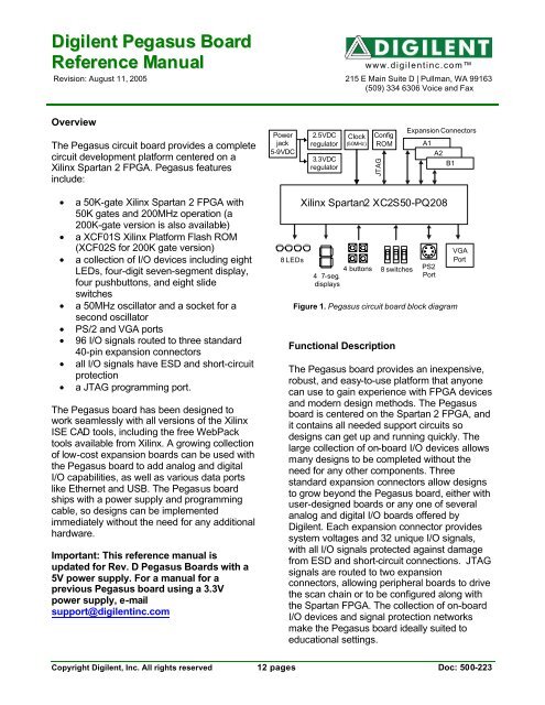
Digilent Pegasus Board Reference Manual - Digilent Inc.
Digilent Pegasus Board Reference Manual - Digilent Inc.
Digilent Pegasus Board Reference Manual - Digilent Inc.

You also want an ePaper? Increase the reach of your titles
YUMPU automatically turns print PDFs into web optimized ePapers that Google loves.
<strong>Pegasus</strong> <strong>Reference</strong> <strong>Manual</strong><strong>Digilent</strong>, <strong>Inc</strong>. The primary oscillator is connected to theGLK1 input of the Spartan 2 (pin 77) and thesecondary oscillator is connected to GCLK2(pin 182). Both clock inputs can drive a DLL onthe Spartan 2, allowing for a wide range ifinternal frequencies are up to four times higherthan the external clock signals. Any 5Voscillator in a half-size DIP package can beloaded into the secondary oscillator socket.Pushbuttons, Slide Switches, and LEDsFour pushbuttons and eight slide switches areprovided for circuit inputs. Pushbutton inputsare normally low, and they are driven high onlywhen the pushbutton is pressed. Slideswitches generate constant high or low inputsdepending on their position. Pushbutton inputsuse RC networks to provide nominal debounceand ESD protection. Slide switch inputs useonly a series resistor for protection.Eight LEDs are provided for circuit outputs.LED anodes are driven directly from the FPGAvia 470-ohm resistors, and the cathodes areconnected directly to ground. A ninth LED isprovided as a power-on LED, and a tenth LEDindicates JTAG programming status.3.3V4.7KohmsPushbuttons4.7K ohms0.1uFTo FPGASeven-Segment DisplayThe <strong>Pegasus</strong> board contains a four-digitcommon anode seven-segment LED display.The display is multiplexed, so only sevencathode signals exist to drive all 28 segmentsin the display. Four digit-enable signals drivethe common anodes and these signalsdetermine which digit the cathode signalsilluminate.Anodes are connected viatransistors for greater currentVddAN3AN2a b c d e fAN1g dpAN0Cathodes are connected toXilinx device via 100Ω resistorsFigure 4. Common anode Sseg displayThe seven anodes of each digit’s LEDs areconnected together into one “common anode”circuit node. The display has four such nodesnamed AN0 – AN3, and the signals that drivethese nodes serve as digit enablers. Driving ananode signal low enables the correspondingdigit. The cathodes of similar segments on allfour displays are connected into seven circuitnodes labeled CA through CG. Driving cathodesignals low illuminates segments on any digitwhose digit enable is low.3.3VCommon anodeSlide switches4.7KohmsTo FPGAfeagbcLEDsFromFPGA390 ohmsFigure 3. Pushbutton, slide switch, and LED circuitsda f g e d c bFigure 5. Common anode detailThis connection scheme creates a multiplexeddisplay, where driving the anode signals andcorresponding cathode patterns of each digit inwww.digilentinc.com Page 3
<strong>Pegasus</strong> <strong>Reference</strong> <strong>Manual</strong><strong>Digilent</strong>, <strong>Inc</strong>. a repeating, continuous succession can createthe appearance of a four-digit display. Each ofthe four digits will appear bright andcontinuously illuminated if the digit enablesignals are driven low once every 1 to 16ms(for a refresh frequency of 1KHz to 60Hz). Forexample, in a 60Hz refresh scheme, each digitwould be illuminated for one quarter of therefresh cycle, or 4ms. The controller mustassure that the correct cathode pattern ispresent when the corresponding anode signalis driven.AN0AN1AN2AN3Digit 0Refresh period = 1ms to 16msDigit period = Refresh / 4Digit 1 Digit 2 Digit 3Figure 6. Sseg signal timingTo illustrate the process, if AN0 is driven lowwhile CB and CC are driven low, then a “1” willbe displayed in digit position 0. Then, if AN1 isdriven low while CA, CB and CC are drivenlow, then a “7” will be displayed in digit position1. If AN0 and CB, CC are driven low for 4 ms,and then AN1 and CA, CB, CC are driven lowfor 4 ms in an endless succession, the displaywill show “71” in the rightmost two digits.Digit Cathode SignalsShown a b c d e f g0 0 0 0 0 0 0 11 1 0 0 1 1 1 12 0 0 1 0 0 1 03 0 0 0 0 1 1 04 1 0 0 1 1 0 05 0 1 0 0 1 0 06 0 1 0 0 0 0 07 0 0 0 1 1 1 18 0 0 0 0 0 0 09 0 0 0 1 1 0 0Figure 7. Cathode patterns for decimal digitsPS/2 PortThe <strong>Pegasus</strong> board includes a 6-pin mini-DINconnector that can accommodate a PS/2mouse or keyboard connection. A jumper onthe <strong>Pegasus</strong> board (J9) can beloaded to provide 5V to the PS/2port, or an external supply can beconnected to the “PS2VCC” pin ofJ9 (some PS/2 devices require 5Vto work properly).PS/2 PowerPin 22 145 3 6PS2 ConnectorPin 6Pin 1Pin 5Bottom-uphole patternFigure 8. PS/2 connectionsPin DefinitionsPin Function1 Data2 Reserved3 GND4 Vdd5 Clock6 ReservedThe PS/2 protocol uses a bi-directional twowireinterface that includes a serial data and aclock signal (the host-to-keyboard datadirection is used to send status LED data).Driver circuits on both ends of the clock anddata signals use open-collector buffers with10K pull-ups. The signals are only driven whena key is actively pressed (or when the host isactively sending LED status data). If the PS/2device is only used as an input device, thenthe host system can just use input buffers(open-collector buffers are not required).PS/2 mouse and keyboard devices use11-bitdata words that include a start bit, eight databits, and odd parity bit, and a stop bit. Datatimings are shown in the figure below. Themouse and keyboard use eight-bit datapackets that are organized differently – thekeyboard sends eight-bit key scan codes, andthe mouse sends three eight-bit data elementsto define relative mouse movements.KeyboardEach key has a single, unique scan code thatis sent whenever the corresponding key ispressed. If a key is continuously pressed formore than 570ms, its scan code is repeatedeach 104ms (but the time interval between firstand second transmission of the same code isJ9VCC33PS2VCCVUwww.digilentinc.com Page 4
<strong>Pegasus</strong> <strong>Reference</strong> <strong>Manual</strong><strong>Digilent</strong>, <strong>Inc</strong>. 570ms). When releasing a key that waspressed for more than 570ms, an “F0” key-upcode is sent, followed immediately by the keyscan code. If a key can be “shifted” to producea new character (like a capital letter), then theshift character is sent before the key scancode. Some keys, called extended keys, sendan “E0” ahead of the scan code (and they maysend more than one scan code). When anextended key is released, an “E0 F0” key-upcode is sent, followed by the scan code.Signals timings and scan codes for most keysare shown in the figure below.A host device can also send data to thekeyboard. Below is a short list of some oftenusedcommands.EDSet Num Lock, Caps Lock, and Scroll LockLEDs. After receiving an “ED”, the keyboardreturns an “FA”. Then the host sends a byteto set LED status: bit 0 sets Scroll Lock, bit 1sets Num Lock, and bit 2 sets Caps Lock.Bits 3 to 7 are ignored.EEF3FEFFEcho. Upon receiving an echo command, thekeyboard replies with “EE”.Set scan code repeat rate. The keyboardacknowledges receipt of an “F3” by returningan “FA”, after which the host sends a secondbyte to set the repeat rate.Resend. Upon receiving FE, the keyboard resendsthe last scan code sent.Reset. Resets the keyboard.The keyboard should send data to the hostonly when both the data and clock lines arehigh (or idle). Since the host is the “busmaster”, the keyboard should check to seewhether the host is sending data before drivingthe bus. To facilitate this, the clock line can beused as a “clear to send” signal. If the hostpulls the clock line low, the keyboard must notsend any data until the clock is released.MouseThe mouse outputs a clock and data signalwhen it is moved; otherwise, these signalsT CK T CKEdge 0 Edge 10CLKT SUT HLDDATA'0' start bit'1' stop bitSymbol Parameter Min MaxT CKT SUClock time30us 50usData-to-clock setup time 5us 25usT HLD Clock-to-data hold time 5us 25us~3.1ms ~570ms ~104msTiming for a two-bytescan codeScan code repeat timing(key pressed and held)Figure 9. PS/2 timingsremain at logic ‘1’. Each time the mouse iswww.digilentinc.com Page 5
<strong>Pegasus</strong> <strong>Reference</strong> <strong>Manual</strong><strong>Digilent</strong>, <strong>Inc</strong>. moved, three 11-bit words are sent from themouse to the host device. Each of the 11-bitwords contains a ‘0’ start bit, followed by eightbits of data (LSB first), followed by an oddparity bit, and terminated with a ‘1’ stop bit.Thus, each data transmission contains 33 bits,where bits 0, 11, and 22 are ‘0’ start bits, andbits 10, 21, and 32 are ‘1’ stop bits. The three8-bit data fields contain movement data asshown below. Data is valid at the falling edgeof the clock, and the clock period is 20 to30KHz.The mouse assumes a relative coordinatesystem wherein moving the mouse to the rightgenerates a positive number in the X field, andmoving to the left generates a negativenumber. Likewise, moving the mouse upgenerates a positive number in the Y field, andmoving down represents a negative number(the XS and YS bits in the status byte are thesign bits – a ‘1’ indicates a negative number).The magnitude of the X and Y numbersrepresent the rate of mouse movement – thelarger the number, the faster the mouse ismoving (the XV and YV bits in the status byteare movement overflow indicators – a ‘1’means overflow has occurred). If the mousemoves continuously, the 33-bit transmissionsare repeated every 50ms or so. The L and Rfields in the status byte indicate left and rightbutton presses (a ‘1’ indicates the button isbeing pressed).Mouse status byte X direction byte Y direction byte10 L R 0 1 XS YS XY YY P 1 0 X0 X1 X2 X3 X4 X5 X6 X7 P 1 0 Y0 Y1 Y2 Y3 Y4 Y5 Y6 Y7 P 1Idle state Start bit Stop bit Start bitStop bitStart bitStop bitIdle stateFigure 10. PS/2 mouse dataVGA PortThe five standard VGA signals red (R), green(G), blue (B), horizontal sync (HS), and verticalync (VS) are routed from FPGA pins to theVGA connector. The color signals passthrough 270-ohm resistors on the <strong>Pegasus</strong>board to create a resistor-divider with the 75-ohm VGA cable termination. This limits thevoltage at the VGA connector to the specified0V (fully-off) to 0.7V (fully-on) range. Thisthree-bit color system allows for eight differentcolors as shown in the table.Color Red Green BlueBlack 0 0 0Blue 0 0 1Green 0 1 0Cyan 0 1 1Red 1 0 0Purple 1 0 1Yellow 1 1 0White 1 1 1Table 1. Three-bit color systemCRT Display Systems BackgroundCathode ray tube (CRT)-based VGA displaysuse amplitude-modulated, moving electronbeams (or cathode rays) to display informationon a phosphor-coated screen. LCD displays usean array of switches that can impose a voltageacross a small amount of liquid crystal, therebychanging light permittivity through the crystal ona pixel-by-pixel basis. Although the followingdescription is limited to CRT displays, LCDdisplays have evolved to use the same signaltimings as CRT displays (so the “signals”discussion below pertains to both CRTs andLCDs).CRT displays use three electron beams (one forred, one for blue, and one for green) to energizethe phosphor that coats the inner side of thedisplay end of a cathode ray tube (see drawingbelow). Electron beams emanate from electronguns, which are finely-pointed heated cathodesplaced in close proximity to a positively chargedannular plate called a “grid”.www.digilentinc.com Page 6
<strong>Pegasus</strong> <strong>Reference</strong> <strong>Manual</strong><strong>Digilent</strong>, <strong>Inc</strong>. The electrostatic force imposed by the gridpulls away rays of energized electrons ascurrent flows into the cathodes. These cathoderays are initially accelerated towards the grid,but they soon fall under the influence of themuch larger electrostatic force that results fromthe entire phosphor-coated display surface ofthe CRT being charged to 20kV (or more). Theparticle rays are focused to a fine beam asthey pass through the center of the grids, andthen they accelerate to impact on thephosphor-coated display surface. Thephosphor surface glows brightly at the impactpoint, and the phosphor continues to glow forseveral hundred microseconds after the beamis removed. The larger the current fed into thecathode, the brighter the phosphor will glow.Between the grid and the display surface, thebeam passes through the neck of the CRTwhere two coils of wire produce orthogonalelectromagnetic fields. Because cathode raysare composed of charged particles (electrons),they can be deflected by these magnetic fields.Current waveforms are passed through thecoils to produce magnetic fields that interactwith the cathode rays and cause them totransverse the display surface in a “raster”pattern, horizontally from left to right andvertically from top to bottom.As the cathode ray moves over the surface ofthe display, the current sent to the electron gunscan be increased or decreased to change thebrightness of the display at the cathode rayimpact point. Information is only displayed whenthe beam is moving in the “forward” direction (leftto right and top to bottom), and not during thetime the beam is reset back to the top left edgeof the display. Much of the potential display timeis therefore lost in “blanking” periods when thebeam is reset and stabilized to begin a newhorizontal or vertical display pass.The size of the beams, the frequency at whichthe beam can be traced across the display, andthe frequency at which the electron beam can bemodulated determine the display resolution.Modern VGA displays can accommodatedifferent resolutions, and a VGA controller circuitdictates the resolution by producing timingsignals to control the raster patterns. Thecontroller must produce synchronizing pulses at5V to set the frequency at which current flowsthrough the deflection coils, and it must ensurethat video data is applied to the electron guns atthe correct time.Raster video displays define a number of “rows”that corresponds to the number of horizontalpasses the cathode makes over the display area,and a number of “columns” that corresponds toan area on each row that is assigned to one“picture element” or pixel. Typical displays useAnode (entire screen)Cathode ray tubeCathode ray tube display systemCathode rayDeflection coilsGridElectron guns(Red, Blue, Green)R,G,B signals (to guns)deflectioncontrolHigh voltage supply (>20kV)gridcontrolControl boardguncontrolSync signals(to deflection control)VGA cablewww.digilentinc.com Page 7
<strong>Pegasus</strong> <strong>Reference</strong> <strong>Manual</strong><strong>Digilent</strong>, <strong>Inc</strong>. from 240 to 1200 rows, and from 320 to 1600columns. The overall size of a display, and thenumber of rows and columns determines thesize of each pixel.Video data typically comes from a videorefresh memory, with one or more bytesassigned to each pixel location (the DIO4board uses three bits per pixel). The controllermust index into video memory as the beamsmove across the display, and retrieve andapply video data to the display at precisely thetime the electron beam is moving across agiven pixel.VGA System TimingVGA signal timings are specified, published,copyrighted, and sold by the VESAorganization (www.vesa.org). The followingVGA system timing information is provided asan example of how a VGA monitor might bedriven in 640 by 480 mode. For more preciseinformation, or for information on higher VGAfrequencies, refer to the VESA website above.A VGA controller circuit must generate the HSand VS timing signals and coordinate thedelivery of video data based on the pixel clock.The pixel clock defines the time available todisplay one pixel of information. The VS signaldefines the “refresh” frequency of the display,i.e., the frequency at which all information onthe display is redrawn. The minimum refreshfrequency is a function of the display’s phosphorand electron beam intensity, with practicalrefresh frequencies falling in the 50Hz to 120Hzrange.The number of lines to be displayed at a givenrefresh frequency defines the horizontal “retrace”frequency. For a 640-pixel by 480-row displayusing a 25MHz pixel clock and 60 +/-1Hzrefresh, the signal timings shown in the tablebelow can be derived. Timings for sync pulsewidth and front and back porch intervals (porchintervals are the pre- and post-sync pulse timesduring which information cannot be displayed)are based on observations taken from VGAdisplays.A VGA controller circuit decodes the output of ahorizontal-sync counter driven by the pixel clockto generate HS signal timings. This counter canbe used to locate any pixel location on a givenrow. Likewise, the output of a vertical-synccounter that increments with each HS pulse canbe used to generate VS signal timings, and thiscounter can be used to locate any given row.These two continually running counters can beused to form an address into video RAM. Notime relationship between the onset of the HSpulse and the onset of the VS pulse is specified,so the designer can arrange the counters toeasily form video RAM addresses, or to minimizeSymbolT ST dispT pwT fpT bpParameterSync pulse timeDisplay timePulse widthFront porchBack porchVertical SyncTime Clocks Lines16.7ms 416,800 52115.36ms64 us320 us928 us384,0001,6008,00023,20048021029Horizontal SyncTime Clocks32 us 80025.6 us 6403.84 us 96640 ns 161.92 us 48T pwT ST dispT fpT bpHSZeroDetectSetCEZeroDetectSetVSHorizontalCounterHorizontalSynchVerticalCounterVerticalSynch3.84usDetectReset64usDetectResetwww.digilentinc.com Page 8
<strong>Pegasus</strong> <strong>Reference</strong> <strong>Manual</strong><strong>Digilent</strong>, <strong>Inc</strong>. System Bus TimingSymbolParameterTime(typ)ten Time to enable after CS asserted 10nsth Hold time 1nstdoe Time to disable after OE deasserted10nsteoe Time to enable after OE asserted 15nstw Write strobe time 10nstsu Data setup time 5nstwd Write disable time 0nsModule Bus TimingSymbolParameterTime(typ)tstb Strobe time 10nstwt Strobe to wait time 10 nstwr Time to enable write 15 nstsu Data setup time 5 nsth Data hold time 5 nsWrite CycleTenThWrite Cycle*CSOEWEDB0-DB7TdoeTwTsuTeoeThASTBDSTBWAITnWRT STBT STBT WRT WTT HT HRead CycleTenThDATAT SUT HCSOEWEDB0-DB7TeoeTwdTsuRead data latch timeTdoeThThRead Cycle*ASTBDSTBWAITT STBT STBT WRT WTT HT HnWRTsuThDATA* ASTB and DSTB determine whether an address orFigure 14. Peripheral bus signals and data timings write cycle occurs. Only one should beasserted for each bus transaction.www.digilentinc.com Page 10
<strong>Pegasus</strong> <strong>Reference</strong> <strong>Manual</strong><strong>Digilent</strong>, <strong>Inc</strong>. <strong>Pegasus</strong> Expansion Connector PinoutConnector B1 Connector A1 Connector A2Pin Signal B1 Pin Signal A1 Pin Signal A239 TDO TDO 39 TDO TDO 39 GCK0 GCK040 TDI TDI 40 TDI TDI 40 GND GND37 TMS TMS 37 TMS TMS 37 n/c n/c38 TCK TCK 38 TCK TCK 38 n/c n/c35 MB1-INIT 90 35 MA1-INIT 189 35 MA2-INT 13836 GND GND 36 GND GND 36 Not used n/c33 MB1-WAIT 95 33 MA1-WAIT 192 33 MA2-WAIT 14034 M1-RST 94 34 M1-RST 191 34 MA2-RST 13931 MB1-DSTB 97 31 MA1-DSTB 194 31 MA2-DSTB 14232 MB1-WRIT 96 32 MA1-WRIT 193 32 MA2-WRIT 14129 MB1-DB7 99 29 MA1-DB7 199 29 MA2-DB7 14730 MB1-ASTB 98 30 MA1-ASTB 195 30 MA2-ASTB 14627 MB1-DB5 101 27 MA1-DB5 201 27 MA2-DB5 14928 MB1-DB6 100 28 MA1-DB6 200 28 MA2-DB6 14825 MB1-DB3 108 25 MA1-DB3 203 25 MA2-DB3 15126 MB1-DB4 102 26 MA1-DB4 202 26 MA2-DB4 15023 MB1-DB1 110 23 MA1-DB1 205 23 MA2-DB1 16024 MB1-DB2 109 24 MA1-DB2 204 24 MA2-DB2 15221 P-LSBCLK 112 21 LSBCLK 3 21 P-IO18 16222 MB1-DB0 111 22 MA1-DB0 206 22 MA2-DB0 16119 P1-DB7 114 19 DB7 5 19 P-IO16 16420 P-CSA 113 20 CSA 4 20 P-IO17 16317 P-DB6 119 17 DB6 7 17 P-IO14 16618 P-OE 115 18 OE 6 18 P-IO15 16515 P-DB5 121 15 DB5 9 15 P-IO12 16816 P-WE 120 16 WE 8 16 P-IO13 16713 P-DB4 123 13 DB4 14 13 P-IO10 17314 P-ADR5 122 14 ADR5 10 14 P-IO11 17211 P-DB3 126 11 DB3 16 11 P-IO8 17512 P-ADR4 125 12 ADR4 15 12 P-IO9 1749 P-DB2 129 9 DB2 18 9 P-IO6 17810 P-ADR3 127 10 ADR3 17 10 P-IO7 1767 P-DB1 133 7 DB1 21 7 P-IO4 1808 P-ADR2 132 8 ADR2 20 8 P-IO5 1795 P-DB0 135 5 DB0 23 5 P-IO2 1876 P-ADR1 134 6 ADR1 22 6 P-IO3 1813 VCCO VCCO 3 VCCO VCCO 3 VCCO VCCO4 P-ADR0 136 4 ADR0 24 4 P-IO1 1881 GND GND 1 GND GND 1 GND GND2 VU VU 2 VU VU 2 VU VUAccessory Port PinoutPin Name FPGA Pin Pin Name FPGA Pin1 AC0 P49 4 AC3 P472 AC1 P48 5 GND -3 AC2 P81 6 Vdd -www.digilentinc.com Page 11
<strong>Pegasus</strong> <strong>Reference</strong> <strong>Manual</strong><strong>Digilent</strong>, <strong>Inc</strong>. <strong>Pegasus</strong> FPGA Pin AssignmentsPin Function Pin Function Pin Function Pin Function1 GND 53 VCCO 105 VCCO 157 TDO2 TMS 54 MODE2 106 PROGRAM 158 GND3 LLSBCLK 55 PB-IO14 107 INIT/IO 159 TDI4 LCSA 56 PB-IO13 108 LMB1-DB3 160 LMA2-DB15 LDB7 57 BTN2 109 LMB1-DB2 161 LMA2-DB06 LOE 58 BTN1 110 LMB1-DB1 162 LPA-IO187 LDB6 59 BTN0 111 LMB1-DB0 163 LPA-IO178 LWE 60 AN0 112 LPB-LSBCLK 164 LPA-IO169 LDB5 61 CE 113 LPB-CSA 165 LPA-IO1510 LADR5 62 CD 114 LPB-DB7 166 LPA-IO1411 GND 63 DP 115 LPB-OE 167 LPA-IO1312 VCCO 64 GND 116 GND 168 LPA-IO1213 VCCINIT 65 VCCO 117 VCCO 169 GND14 LDB4 66 VCCINIT 118 VCCINIT 170 VCCO15 LADR4 67 CC 119 LPB-DB6 171 VCCINIT16 LDB3 68 CG 120 LPB-WE 172 LPA-IO1117 LADR3 69 AN1 121 LPB-DB5 173 LPA-IO1018 LDB2 70 CB 122 LPB-ADR5 174 LPA-IO919 GND 71 AN2 123 LPB-DB4 175 LPA-IO820 LADR2 72 GND 124 GND 176 LPA-IO721 LDB1 73 CF 125 LPB-ADR4 177 GND22 LADR1 74 CA 126 LPB-DB3 178 LPA-IO623 LDB0 75 AN3 127 LPB-ADR3 179 LPA-IO524 LADR0 76 VCCINIT 128 VCCINIT 180 LPA-IO425 GND 77 GCK1 129 LPB-DB2 181 LPA-IO326 VCCO 78 VCCO 130 VCCO 182 GCK227 VS 79 GND 131 GND 183 GND28 VCCINT 80 GCK0 132 LPB-ADR2 184 VCCO29 HS 81 SW7/AC2 133 LPB-DB1 185 GCK330 BLUE 82 SW6 134 LPB-ADR1 186 VCCINIT31 GRN 83 SW5 135 LPB-DB0 187 LPA-IO232 GND 84 SW4 136 LPB-ADR0 188 LPA-IO133 RED 85 GND 137 GND 189 LMA1-INT34 PS2C 86 SW3 138 LMA2-INT 190 GND35 PS2D 87 SW2 139 LMA2-RESET 191 LMA1-RESET36 LD7 88 SW1 140 LMA2-WAIT 192 LMA1-WAIT37 LD6 89 SW0 141 LMA2-WRITE 193 LMA1-WRITE38 VCCINIT 90 LMB1-INT 142 LMA2-DSTB 194 LMA1-DSTB39 VCCO 91 VCCINIT 143 VCCINIT 195 LMA1-ASTB40 MC1-DB4 92 GND 144 VCCO 196 VCCINIT41 LD5 93 GND 145 GND 197 VCCO42 LD4 94 LMB1-RESET 146 LMA2-ASTB 198 GND43 LD3 95 LMB1-WAIT 147 LMA2-DB7 199 LMA1-DB744 LD2 96 LMB1-WRITE 148 LMA2-DB6 200 LMA1-DB645 LD1 97 LMB1-DSTB 149 LMA2-DB5 201 LMA1-DB546 LD0 98 LMB1-ASTB 150 LMA2-DB4 202 LMA1-DB447 AC3 99 LMB1-DB7 151 LMA2-DB3 203 LMA1-DB348 AC1 100 LMB1-DB6 152 LMA2-DB2 204 LMA1-DB249 AC0 101 LMB1-DB5 153 DIN/D0/IO 205 LMA1-DB150 MODE1 102 LMB1-DB4 154 BTN3 206 LMA1-DB051 GND 103 GND 155 CCLK 207 TCK52 MODE0 104 DONE 156 VCCO 208 VCCOwww.digilentinc.com Page 12