VITA 46.9: Ensuring mezzanine I/O pinout interoperability for VPX ...
VITA 46.9: Ensuring mezzanine I/O pinout interoperability for VPX ...
VITA 46.9: Ensuring mezzanine I/O pinout interoperability for VPX ...

Create successful ePaper yourself
Turn your PDF publications into a flip-book with our unique Google optimized e-Paper software.
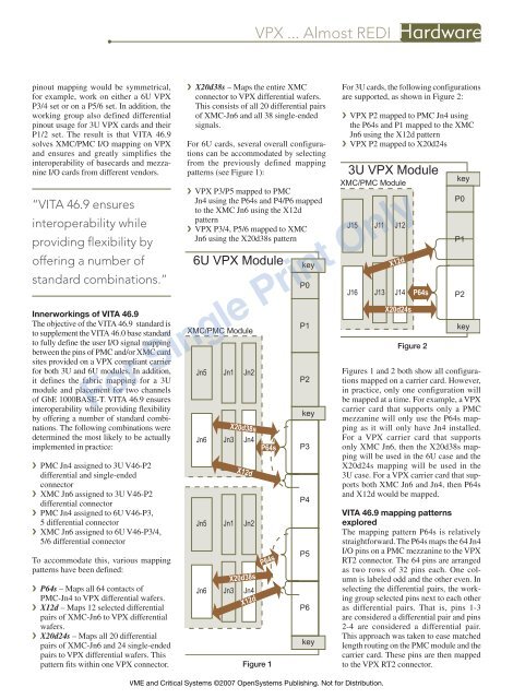
<strong>VPX</strong> ... Almost REDIHardware<strong>pinout</strong> mapping would be symmetrical,<strong>for</strong> example, work on either a 6U <strong>VPX</strong>P3/4 set or on a P5/6 set. In addition, theworking group also defined differential<strong>pinout</strong> usage <strong>for</strong> 3U <strong>VPX</strong> cards and theirP1/2 set. The result is that <strong>VITA</strong> <strong>46.9</strong>solves XMC/PMC I/O mapping on <strong>VPX</strong>and ensures and greatly simplifies the<strong>interoperability</strong> of basecards and <strong>mezzanine</strong>I/O cards from different vendors.“<strong>VITA</strong> <strong>46.9</strong> ensures<strong>interoperability</strong> whileproviding flexibility byoffering a number ofstandard combinations.”Innerworkings of <strong>VITA</strong> <strong>46.9</strong>The objective of the <strong>VITA</strong> <strong>46.9</strong> standard isto supplement the <strong>VITA</strong> 46.0 base standardto fully define the user I/O signal mappingbetween the pins of PMC and/or XMC cardsites provided on a <strong>VPX</strong> compliant carrier<strong>for</strong> both 3U and 6U modules. In addition,it defines the fabric mapping <strong>for</strong> a 3Umodule and placement <strong>for</strong> two channelsof GbE 1000BASE-T. <strong>VITA</strong> <strong>46.9</strong> ensures<strong>interoperability</strong> while providing flexibilityby offering a number of standard combinations.The following combinations weredetermined the most likely to be actuallyimplemented in practice: PMC Jn4 assigned to 3U V46-P2differential and single-endedconnector XMC Jn6 assigned to 3U V46-P2differential connector PMC Jn4 assigned to 6U V46-P3,5 differential connector XMC Jn6 assigned to 6U V46-P3/4,5/6 differential connectorTo accommodate this, various mappingpatterns have been defined: P64s – Maps all 64 contacts ofPMC-Jn4 to <strong>VPX</strong> differential wafers. X12d – Maps 12 selected differentialpairs of XMC-Jn6 to <strong>VPX</strong> differentialwafers. X20d24s – Maps all 20 differentialpairs of XMC-Jn6 and 24 single-endedpairs to <strong>VPX</strong> differential wafers. Thispattern fits within one <strong>VPX</strong> connector. X20d38s – Maps the entire XMCconnector to <strong>VPX</strong> differential wafers.This consists of all 20 differential pairsof XMC-Jn6 and all 38 single-endedsignals.For 6U cards, several overall configurationscan be accommodated by selectingfrom the previously defined mappingpatterns (see Figure 1): <strong>VPX</strong> P3/P5 mapped to PMCJn4 using the P64s and P4/P6 mappedto the XMC Jn6 using the X12dpattern <strong>VPX</strong> P3/4, P5/6 mapped to XMCJn6 using the X20d38s pattern6U <strong>VPX</strong> ModuleXMC/PMC ModuleJn5 Jn1 Jn2Jn6Jn3X20d38sJn4X12dJn5 Jn1 Jn2X20d38sJn6 Jn3 Jn4X12dP64sP64sFigure 1keyP0P1P2keyP3P4P5P6keyFor 3U cards, the following configurationsare supported, as shown in Figure 2: <strong>VPX</strong> P2 mapped to PMC Jn4 usingthe P64s and P1 mapped to the XMCJn6 using the X12d pattern <strong>VPX</strong> P2 mapped to X20d24s3U <strong>VPX</strong> ModuleXMC/PMC ModuleJ15 J11 J12J16J13X12dJ14X20d24sP64sFigure 2keyP0P1P2keyFigures 1 and 2 both show all configurationsmapped on a carrier card. However,in practice, only one configuration willbe mapped at a time. For example, a <strong>VPX</strong>carrier card that supports only a PMC<strong>mezzanine</strong> will only use the P64s mappingas it will only have Jn4 installed.For a <strong>VPX</strong> carrier card that supportsonly XMC Jn6, then the X20d38s mappingwill be used in the 6U case and theX20d24s mapping will be used in the3U case. For a <strong>VPX</strong> carrier card that supportsboth XMC Jn6 and Jn4, then P64sand X12d would be mapped.ForSinglePrintOnlyVME and Critical Systems ©2007 OpenSystems Publishing. Not <strong>for</strong> Distribution.<strong>VITA</strong> <strong>46.9</strong> mapping patternsexploredThe mapping pattern P64s is relativelystraight<strong>for</strong>ward. The P64s maps the 64 Jn4I/O pins on a PMC <strong>mezzanine</strong> to the <strong>VPX</strong>RT2 connector. The 64 pins are arrangedas two rows of 32 pins each. One columnis labeled odd and the other even. Inselecting the differential pairs, the workinggroup selected pins next to each otheras differential pairs. That is, pins 1-3are considered a differential pair and pins2-4 are considered a differential pair.This approach was taken to ease matchedlength routing on the PMC module and thecarrier card. These pins are then mappedto the <strong>VPX</strong> RT2 connector.