Embedded Computing Design - OpenSystems Media
Embedded Computing Design - OpenSystems Media
Embedded Computing Design - OpenSystems Media

You also want an ePaper? Increase the reach of your titles
YUMPU automatically turns print PDFs into web optimized ePapers that Google loves.
RSC #2 @ www.embedded-computing.com/rsc
RSC #3 @ www.embedded-computing.com/rsc
W W W. E M B E D D E D - C O M P U T I N G. C O M<br />
Vo l u m e 2 • N u m b e r 2<br />
S U M M E R 2 0 0 4<br />
CONTENTS<br />
COLUMNS<br />
7 Editor’s Foreword<br />
Switch fabrics move forward ...<br />
By Mark David Barrera<br />
8 Industry Report<br />
By Bonnie Crutcher<br />
12 Book Review<br />
ARM System Developer’s Guide<br />
By Andrew N. Sloss, Dominic Symes, and Chris Wright<br />
14 EEMBC<br />
Standardizing a powerful measurement<br />
By Markus Levy<br />
16 ZigBee Alliance<br />
Networking with Zigbee<br />
By Jon Adams<br />
19 Linux News<br />
By Bonnie Crutcher<br />
61 New Products<br />
By Eli Shapiro<br />
EVENTS<br />
SUPERCOMM<br />
June 20-24, 2004 • Chicago, Illinois<br />
www.supercomm2004.com<br />
Real-Time & <strong>Embedded</strong> <strong>Computing</strong> Conference (RTECC)<br />
June 30, 2004 • Greenbelt<br />
August 17, 2004 • Dayton<br />
www.rtecc.com<br />
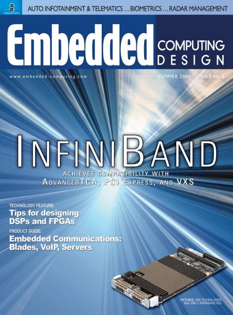
Product photo credit:<br />
SBS Technologies IB4X-PMC-2<br />
InfiniBand 4x Dual-Port PMC Host<br />
Channel Adapter (HCA)<br />
<strong>Embedded</strong><br />
<strong>Computing</strong><br />
<strong>Design</strong><br />
published by:<br />
www<br />
e m b e d d e d - c o m p u t i n g . c o m<br />
4 / Summer 2004 <strong>Embedded</strong> <strong>Computing</strong> <strong>Design</strong><br />
<strong>OpenSystems</strong><br />
Publishing TM<br />
FEATURES<br />
SPECIAL: Fabric Diversity<br />
20 InfiniBand and PCI-Express subsystems:<br />
A winning combination for embedded applications<br />
By Lori Dunbar and Steve Cook, SBS Technologies<br />
25 The current landscape of switch fabrics and RapidIO<br />
By Luc Torres, Thales Computers<br />
TECHNOLOGY: <strong>Design</strong> Tips<br />
30 Tips for designing DSPs and FPGAs<br />
By Eric Cigan, AccelChip<br />
36 Tips for designing complex FPGAs<br />
By Salil Raje, Hier <strong>Design</strong><br />
42 Leveraging FPGA coprocessors to optimize automotive<br />
infotainment and telematics systems<br />
By Paul Ekas, Altera<br />
APPLICATION: Biometrics<br />
49 New fingerprint subsystem brings biometrics to the<br />
mass market<br />
By Kevin C. Kreitzer, Analog Devices, Inc.<br />
and Alan Kasten, AuthenTec, Inc.<br />
52 Government Security<br />
Surveillance and control systems for the modern military<br />
By Steve Wigent, Performance Technologies<br />
PRODUCT GUIDE: <strong>Embedded</strong> Communications<br />
55 Blades – Servers – VoIP<br />
By Chad Lumsden<br />
E-LETTERS ONLINE<br />
July E-letter: Making the Switch to RapidIO<br />
by Paul N. Leroux, QNX Software Systems Ltd.<br />
www.embedded-computing.com/eletter<br />
FREE SUBSCRIPTIONS<br />
Subscribe to the magazine or E-letter, or change your<br />
subscription at: www.opensystems-publishing.com/subscriptions<br />
© 2004 <strong>Embedded</strong> <strong>Computing</strong> <strong>Design</strong>
And you thought SHE was<br />
sensitive<br />
What about your embedded<br />
system<br />
Just like sensing the pea under a<br />
mattress, your A/D and D/A system<br />
must detect and measure accurately<br />
too. So, start your system design<br />
with boards that handle real world<br />
irritants like temperature, drift and<br />
electrical noise.<br />
Sleep easier knowing your<br />
measurements are accurate<br />
because the effective number of<br />
bits for the whole system is close<br />
to the ideal 12, 14, 16, or 24-bit<br />
resolution of the A/D silicon.<br />
Benefit from onboard fault protection<br />
circuits that ease system<br />
integration by handling the noise<br />
and power sequencing challenges<br />
common to multi-board designs.<br />
Eliminate the need for cumbersome<br />
and complicated layers of auto-<br />
calibration software with our low<br />
drift specs designed to keep your<br />
measurements constant over time.<br />
And our wide selection of cost<br />
sensitive A/D and D/A boards is<br />
something that will make any<br />
princess happy.<br />
We invite you to check out our<br />
12, 14, 16 and 24-bit A/D and D/A<br />
single board computers from<br />
12MHz to 533MHz,<br />
including VGA,<br />
CompactFlash, ®<br />
Ethernet, GPS, CAN, wireless,<br />
and the operating system of your<br />
choice.<br />
Call now and let our technical<br />
team help smooth out those<br />
sensitive issues in your system.<br />
3730 Park Place, Montrose, CA 91020<br />
Voice (818) 244-4600 Fax (818) 244-4246<br />
info@embeddedsys.com<br />
www.embeddedsys.com<br />
EBX<br />
EPIC TM<br />
PC/104<br />
24-bit A/D<br />
Our MPC624 provides 24-bit A/D<br />
for PC/104 with four channels of<br />
instrument grade voltage measurement<br />
and/or four channels of direct<br />
connect to off-the-shelf sensors.<br />
16-bit A/D, 14-bit D/A<br />
Our headless Pentium, ® the SBC2596,<br />
offers Ethernet, GPS, CAN, DC/DC<br />
converter, and CompactFlash on<br />
EBX form factor with full 16-bit<br />
A/D and 14-bit D/A.<br />
14-bit A/D, 14-bit D/A<br />
Our SBC4495 is a 486/586 EPIC<br />
form factor with 14-bit A/D and D/A,<br />
VGA/Flat Panel, PCMCIA, wireless,<br />
and GPS.<br />
For more fully-featured A/D and D/A<br />
SBC boards, visit our web site.<br />
©2004 Micro/sys. All brand and/or product names listed are registered trademarks of their respective owners.
W W W. E M B E D D E D - C O M P U T I N G. C O M<br />
An <strong>OpenSystems</strong> Publication<br />
F<br />
R<br />
E<br />
E<br />
I<br />
N<br />
F<br />
O<br />
R<br />
M<br />
A<br />
T<br />
I<br />
O<br />
N<br />
e<br />
ISSN: Print 1542-6408, Online 1542-6459<br />
<strong>Embedded</strong> <strong>Computing</strong> <strong>Design</strong> is published quarterly by <strong>OpenSystems</strong> Publishing LLC.,<br />
30233 Jefferson Ave., St. Clair Shores, MI 48082.<br />
Subscriptions are free, upon request in writing, to persons dealing with or considering<br />
<strong>Embedded</strong> <strong>Computing</strong> <strong>Design</strong>. For others inside the U.S. and Canada, subscriptions are<br />
$24/year. For 1st class delivery outside the U.S. and Canada, subscriptions are $50/year<br />
(advance payment in U.S. funds required).<br />
Canada: Publication agreement number 40048627<br />
Return address: WDS, Station A, PO Box 54, Windsor, ON N9A 615<br />
POSTMASTER: Send address changes to<br />
<strong>Embedded</strong> <strong>Computing</strong> <strong>Design</strong><br />
13253 La Montana, Suite 207<br />
Fountain Hills, AZ 85268<br />
SALES OFFICE 586-415-6500<br />
VP OF MARKETING & SALES<br />
Patrick Hopper<br />
phopper@opensystems-publishing.com<br />
SENIOR ACCOUNT MANAGER<br />
Dennis Doyle<br />
ddoyle@opensystems-publishing.com<br />
PRINT/ONLINE MARKETING SPECIALIST<br />
Christine Long<br />
clong@opensystems-publishing.com<br />
6 / Summer 2004 <strong>Embedded</strong> <strong>Computing</strong> <strong>Design</strong><br />
ACCOUNT MANAGER<br />
Tom Varcie<br />
tvarcie@opensystems-publishing.com<br />
MARKETING REPRESENTATIVE<br />
Andrea Stabile<br />
astabile@opensystems-publishing.com<br />
FOR REPRINTS:<br />
Call the Sales Office<br />
<strong>OpenSystems</strong><br />
Publishing TM<br />
A D V E R T I S E R I N D E X<br />
Page/RSC# Advertiser Page/RSC# Advertiser<br />
18 AAEON Electronics – PCM-8500 Compact<br />
Board<br />
3701 ABIA – Cube Systems & Low Power<br />
Solutions<br />
63 ACCES I/O Products – PC/104 Analog,<br />
Digital, Relay and Serial Boards<br />
9 Acrosser Technology – 486 PC/104<br />
22 ACT/Technico – Switched Fabric Ethernet<br />
66 Advantech – Ruggedized PC Solutions<br />
35 Analog Devices – Blackfin Processor<br />
4702 Arcom Control Systems – XScale Based<br />
Single Board Computers<br />
5903 Argon Technology Corporation – Managed<br />
PC Boot Agent<br />
64 ARM – ARM Developers’ Conference<br />
62 Artesyn Technologies – ATCA and AMC<br />
24 Bustronic – Switched Fabrics<br />
6502 CG Mupac – StarFabric-Enabled Solutions<br />
7 Concurrent Technologies – VME &<br />
CompactPCI Single Board Computers<br />
67 Continuous <strong>Computing</strong> – Converging<br />
<strong>Computing</strong> and Communications<br />
11 Diamond Systems – <strong>Embedded</strong> Computer<br />
Boards<br />
13 Diversified Technology – Platforms<br />
26 <strong>Embedded</strong> Planet – <strong>Embedded</strong> PowerPC<br />
Control<br />
27 Evalue Technology – Applied <strong>Computing</strong><br />
Solutions<br />
29 Force Computers – Commercial, Rugged<br />
Board and System-Level Products<br />
38 GET Engineering – Naval Tactical Data<br />
Systems<br />
21 Grid Connect – Ethernet On A Chip<br />
40 Intel – <strong>Embedded</strong> Intel Architecture<br />
14 ITCN – VME Chassis and Mil-Std-1553 Busses<br />
5902 JK microsystems – <strong>Embedded</strong> Ethernet<br />
3702 Kontron – Systems<br />
39 Kontron – PICMG<br />
41 Kontron – Modules<br />
43 Kontron – Global Source for <strong>Embedded</strong><br />
<strong>Computing</strong> Technology<br />
51 Lanner Electronics – <strong>Embedded</strong> Platforms<br />
5901 Linux Devices – <strong>Embedded</strong> Linux<br />
19 MEN Micro – SBCs for VME, cPCI, PC/104+<br />
and Computers-On-Modules.<br />
5 Micro/Sys – 12, 14, 16, and 24-bit A/D and D/D<br />
Single Board Computers<br />
17 RLC – <strong>Embedded</strong> Controllers<br />
53 SBE – Boards: WAN, LAN, Storage, Custom<br />
2 SBS Technologies – Single Board Computers<br />
30 Sealevel Systems – Relio Systems<br />
6501 Technologic – 586 Single Board Computer<br />
61 Themis Computer – UltraSPARC COTS<br />
Solutions<br />
48 Titan – Video, Imaging and Graphics<br />
60 TME – <strong>Embedded</strong> Computer Solutions<br />
15 TME – <strong>Embedded</strong> Computer Solutions<br />
32 TME – <strong>Embedded</strong> Computer Solutions<br />
46 Tri-M Systems – Hardware Solutions for<br />
<strong>Embedded</strong> Systems<br />
54 Ultimate Solutions – Development Tools<br />
68 VersaLogic – OEM Product<br />
4701 Windows For Devices – <strong>Embedded</strong><br />
Community<br />
3 WinSystems – Systems Components<br />
PUBLISHERS<br />
John Black, Michael Hopper, Wayne Kristoff<br />
ADVERTISING/BUSINESS OFFICE<br />
30233 Jefferson Avenue<br />
St. Clair Shores, MI 48082<br />
Tel : 586-415-6500 • Fax: 586-415-4882<br />
EDITORIAL/PRODUCTION OFFICE<br />
13253 La Montana, Suite 207<br />
Fountain Hills, Arizona 85268<br />
Tel : 480-967-5581 • Fax: 480-837-6466<br />
SENIOR TECHNICAL EDITOR<br />
Mark David Barrera<br />
mbarrera@opensystems-publishing.com<br />
TECHNICAL EDITOR<br />
Chad Lumsden<br />
clumsden@opensystems-publishing.com<br />
NEWS EDITOR<br />
bicrutcher@opensystems-publishing.com<br />
NEW PRODUCTS EDITOR<br />
Eli Shapiro<br />
newproducts@opensystems-publishing.com<br />
ASSOCIATE EDITOR<br />
Anne Fisher<br />
VICE PRESIDENT OF EDITORIAL<br />
Rosemary Kristoff<br />
rkristoff@opensystems-publishing.com<br />
MANAGING EDITOR<br />
Bonnie Crutcher<br />
CONTRIBUTING WRITERS<br />
Jon Adams<br />
Markus Levy<br />
SENIOR DESIGNER<br />
Joann Toth<br />
SENIOR WEB DESIGNER<br />
Konrad Witte<br />
WEB DESIGNER<br />
Eric Okorie<br />
BUSINESS MANAGER<br />
Karen Layman<br />
CIRCULATION/OFFICE MANAGER<br />
Phyllis Thompson<br />
subscriptions@opensystems-publishing.com<br />
© 2004 <strong>Embedded</strong> <strong>Computing</strong> <strong>Design</strong>
S<br />
Switch fabrics<br />
Welcome to the special switch fabrics edition of <strong>Embedded</strong> <strong>Computing</strong> <strong>Design</strong>. This issue illustrates the ongoing intensive<br />
development of switch fabrics.<br />
The InfiniBand and PCI-Express feature, by Lori Dunbar and Steve Cook of SBS Technologies, is an in-depth discussion of<br />
connectivity issues with an emphasis on InfiniBand.<br />
The switch fabric and RapidIO landscape feature, by Luc Torres of Thales Computers, is also an in-depth connectivity discussion,<br />
but with an emphasis on RapidIO.<br />
DThese articles point out the ongoing discussions in the development of intersystem and intrasystem connections.<br />
B<br />
R<br />
Switch fabrics move forward...<br />
<strong>Design</strong> tips<br />
This issue also includes useful design information for semiconductor and system engineers.<br />
The DSP and FPGA design tips article, by Eric Cigan of AccelChip, is an overview of the benefits of using FPGAs in DSP design,<br />
and concludes with a list of recommended design rules.<br />
The complex FPGA design tips article, by Salil Raje of Hier <strong>Design</strong>, discusses advanced design topics including the benefits of<br />
early design analysis.<br />
The FPGA coprocessor article, by Paul Ekas of Altera, provides valuable information on automotive infotainment and telematic<br />
system optimization, and cost reduction.<br />
Biometrics<br />
The fingerprint recognition system article, by Kevin Kreitzer of Analog Devices, and Alan Kasten of AuthenTec, describes the<br />
development and operation of an embedded biometrics application.<br />
Radar management<br />
The radar information management article, by Steve Wigent of Performance Technologies, describes<br />
an example of the use of embedded systems in critical military applications.<br />
I hope you will find my debut issue as Sr. Technical Editor of <strong>Embedded</strong> <strong>Computing</strong> <strong>Design</strong> to be a<br />
useful addition to your engineering publications library. I encourage your comments and suggestions<br />
concerning this, and future issues.<br />
Mark David Barrera<br />
Sr. Technical Editor<br />
<strong>Embedded</strong> <strong>Computing</strong> <strong>Design</strong> Magazine<br />
mbarrera@opensystems-publishing.com<br />
Mark David Barrera<br />
RSC #7 @ www.embedded-computing.com/rsc<br />
<strong>Embedded</strong> <strong>Computing</strong> <strong>Design</strong> Summer 2004 / 7
icrutcher@opensystems-publishing.com<br />
■ INDUSTRY NEWS<br />
Rugged mobile tablet PC use expected to rise<br />
IMS Research’s most recent survey found that users of rugged<br />
mobile computers expect their consumption of tablet PCs to<br />
significantly increase during the next three years. According to<br />
IMS, this finding confirms the trend that tablet PCs will become<br />
more widely accepted in the rugged mobile computer market.<br />
An IMS survey of companies that purchased rugged mobile<br />
computers found that some 17.6 percent expected to buy tablet<br />
PCs within three years, a significant increase over current market<br />
penetration.<br />
As IMS Research analyst and report author Tim Dawson points<br />
out, “Tablet PCs are a versatile alternative to rugged handheld and<br />
vehicle-fixed PC solutions. The nature of these products means that<br />
they can be used in both handheld and vehicle-fixed applications.”<br />
For more information: www.imsresearch.com<br />
AMI Semiconductor reports record revenues<br />
in 2003<br />
AMI Semiconductor (AMIS), a designer and manufacturer of<br />
integrated mixed-signal and structured digital products for the<br />
automotive, medical, and industrial sectors, reported record<br />
revenues of $454 million in 2003, up from $345 million in 2002,<br />
helped by a strong fourth quarter. The company experienced<br />
revenue growth in each of its target end markets with communications<br />
up 56 percent and automotive, medical, and industrial<br />
growing 44, 27, and 21 percent respectively. AMIS also reported<br />
a 34 percent growth in three-year revenue from design wins<br />
over 2002.<br />
“2003 proved to be a banner year for AMI Semiconductor in all<br />
facets of the company, including our successful IPO,” said Christine<br />
King, President and CEO of AMIS.<br />
For more information: www.amis.com<br />
Augmentix closes $3 million in funding<br />
Augmentix, a provider of enhanced commercial servers for missioncritical<br />
applications, recently announced that it has closed a round<br />
of funding from Austin Ventures. An initial capital investment of<br />
$3 million will allow Augmentix to bring to market its first products,<br />
which have been in development for more than a year.<br />
“Our preliminary meetings with enthusiastic prospects have<br />
confirmed the validity of our approach to building cost-effective<br />
mission-critical servers,” said Augmentix President and CEO<br />
Chris Melson. “With the support of Austin Ventures, we can now<br />
focus on delivering systems that will enable telecommunications,<br />
government agencies, industrial automation, and medical imaging<br />
companies to keep their most demanding and important applications<br />
running without interruption.”<br />
For more information: www.augmentix.com<br />
Data I/0 announces programming support for<br />
Texas Instruments’ digital signal controller<br />
Data I/O, a provider of manual and automated programming<br />
systems, announced high volume programming support for Texas<br />
Instruments’ TMS320F2810 digital signal controller on its Sprint<br />
family of device programmers.<br />
“We are pleased to announce this support for the F2810,” said<br />
Bruce Rodgers, Data I/O Director of Semiconductor Relations<br />
and Marketing. “The automotive market is an important customer<br />
group for our company, and we expect many users will embrace<br />
this family of TI devices for their range of applications.”<br />
For more information: www.data-io.com<br />
MIPS Technologies verifies newest 24K<br />
processor family with Mentor Graphics’<br />
Vstation TBX accelerator<br />
MIPS Technologies, Inc. and Mentor Graphics Corp. recently<br />
announced that the performance of the MIPS32 24K family of<br />
processors, which operates from 400 MHz to 550 MHz worst case<br />
in a 0.13-micron process, was verified using the Mentor Graphics<br />
Vstation TBX verification accelerator.<br />
“With Mentor Graphics’ verification accelerator, we were able to<br />
boot both Linux and the Windows CE .NET operating systems. We<br />
ran thousands of tests and 1.8 billion random verification cycles<br />
per day while still meeting our internal delivery schedule. With<br />
this level of verification quality, we are delivering a 24K core that<br />
is proven, solid, and reliable,” said Don Ramsey, Director of CAD<br />
operations at MIPS Technologies.<br />
For more information: www.mentor.com<br />
WIN Enterprises unveils new website<br />
WIN Enterprises, Inc., a designer and manufacturer of embedded<br />
systems for OEMs, has unveiled www.win-ent.com, to highlight<br />
its design and manufacturing expertise.<br />
According to the company, every service required for x86-based<br />
electronic product development is outlined on the new site. The<br />
site features in-depth product information, an expanded services<br />
section, several case studies, and a Request for Quotation<br />
(RFQ) form.<br />
For more information: www.win-ent.com<br />
Sun adds SSE support to Solaris<br />
Sun has released its quarterly update for the Solaris version of<br />
the UNIX operating system, adding support for several Intel<br />
processor features and for Sun’s new UltraSparc IV processor,<br />
the company announced recently. The new version runs faster on<br />
x86 chips including Intel’s Xeon and Advanced Micro Devices’<br />
Opteron through support for Streaming SIMD Extensions (SSE)<br />
technology, which speeds operations by letting a chip run a single<br />
instruction on multiple data elements.<br />
Sun said the support is included both in Solaris itself and in its Java<br />
software and announced that server maker Rackable Systems will<br />
offer the x86 version of Solaris on its products.<br />
For more information: www.sun.com<br />
8 / Summer 2004 <strong>Embedded</strong> <strong>Computing</strong> <strong>Design</strong>
RSC #9 @ www.embedded-computing.com/rsc
Systran Corporation’s FibreXtreme Serial<br />
FPDP links increase to 50 kilometers<br />
Systran Corporation, a wholly owned subsidiary of Curtiss-Wright<br />
Controls, Inc. and the originator of the Serial FPDP protocol and<br />
developer of the FibreXtreme Serial FPDP data link, today further<br />
extended the reach of their SL100/SL240 Serial FPDP connections<br />
to up to 50 kilometers. The extension increases the original<br />
connection distance by 500 percent. According to the company,<br />
the increase enables designers of radar systems, targeting systems,<br />
and other sensor-to-processor systems to significantly increase the<br />
physical separation of the sensor and the DSP system for safety and<br />
increased system reliability.<br />
For more information: www.systran.com<br />
■ CONFERENCES & AWARDS<br />
Wireless Sensing Solutions advisory board<br />
members announced<br />
IDG World Expo, a producer of tradeshows for technology<br />
markets, and FuelDog Events, a developer of tradeshow concepts<br />
and solutions, recently announced members of the advisory board<br />
for Wireless Sensing Solutions, a new event for the burgeoning<br />
industry of wireless sensor networking. The advisory board will be<br />
responsible for developing a comprehensive program focused on<br />
the standards, interoperability, technologies, and product strategy<br />
driving the wireless sensor networking industry.<br />
Wireless Sensing Solutions will debut September 21-22, 2004 at<br />
the Donald E. Stephens Convention Center in Rosemont, IL.<br />
“The Wireless Sensing Solutions conference answers the very real<br />
need for education about the great advances achieved in wireless<br />
sensing and mesh networking technologies of late,” said advisory<br />
board member Ian Barkin, Managing Director of The FocalPoint<br />
Group. “We are excited to be an integral part of it.”<br />
For more information: www.wssconference.com<br />
■ MERGERS & ACQUISITIONS<br />
Mercury Computer acquires TGS Group<br />
Mercury Computer Systems recently announced the acquisition<br />
of TGS Group, a software developer of 3D image applications<br />
for medical imaging, biotech, oil and gas exploration, and other<br />
industries.<br />
The acquisition is for approximately $18.5 million, consisting of<br />
$6.0 million in Mercury common stock and the remainder in cash,<br />
subject to closing adjustments. The transaction is expected to close<br />
by June 30, 2004, the end of Mercury’s fiscal year.<br />
TGS will enable Mercury to develop integrated technology products<br />
for high-growth 3D imaging markets that include TGS software<br />
and Mercury’s high-performance signal and image processing<br />
multi-computers.<br />
For more information: www.mc.com<br />
Elma acquires Optima EPS<br />
Elma Electronic, Inc., a global manufacturer of electronic<br />
packaging products and rotary components, recently announced<br />
it has acquired Optima Electronic Packaging Systems, a cabinet<br />
enclosure design and manufacturing division of the Gichner<br />
Systems Group, Inc. The name will be changed to Optima EPS<br />
Corp. Components.<br />
“The acquisition of Optima provides us with a reputable,<br />
established, high quality cabinet enclosure line with expertise<br />
in customization services,” said Fred Ruegg, President of Elma<br />
Electronic, Inc. “This product line is an excellent complement to<br />
Elma’s design and manufacturing expertise in electronic hardware<br />
components, subrack enclosures, and system platforms.”<br />
For more information: www.elma.com<br />
■ PEOPLE<br />
DRS Technologies names Joseph E. Hart as<br />
vice president of marketing, aviation, and<br />
unmanned programs<br />
DRS Technologies, Inc. announced recently that Joseph E. Hart<br />
has been named Vice President of marketing, aviation, and<br />
unmanned programs, at the company’s Washington Operations in<br />
Arlington, VA.<br />
In this new position, Hart will oversee the Washington area<br />
marketing of all U.S. Navy, Marine Corps, and Air Force aviation<br />
programs, as well as all product lines associated with unmanned<br />
vehicle technology, including air, land, and maritime surface and<br />
subsurface. He joined DRS in 2002.<br />
“We are pleased to welcome Joe Hart to our Washington office.<br />
His extensive aviation experience adds tremendous depth to our<br />
team,” said Mike Bowman, the Senior Vice President of DRS’s<br />
Washington operations. “A key contributor to the development of<br />
the company’s unmanned technologies business, he successfully<br />
managed the launch of our Sentry Unmanned Aerial Vehicle (UAV)<br />
product line and was instrumental in fully developing and recently<br />
delivering the new Neptune UAV to our US Navy customer.”<br />
For more information: www.drs.com<br />
Aonix selects Ben Goodwin as COO and<br />
VP of sales North America<br />
Aonix has appointed Ben Goodwin as Chief Operations Officer<br />
and Vice President of sales for North America and the Pacific<br />
Rim. Goodwin is directly tasked with strengthening Aonix’s<br />
presence in the United States.<br />
“We are very pleased to welcome Ben back into the Aonix<br />
leadership team,” said Nicolas Hadjidakis, CEO and President of<br />
Aonix. “North America is an important market for Aonix. With<br />
Ben’s strong relationships and extensive experience in the missionand<br />
safety-critical space, we look forward to extending our US<br />
position not only in the military and aerospace industries, but also<br />
in transportation, avionics, telecom, and industrial control, where<br />
similarly complex, critical applications exist.”<br />
For more information: www.aonix.com<br />
■<br />
■<br />
■<br />
10 / Summer 2004 <strong>Embedded</strong> <strong>Computing</strong> <strong>Design</strong>
RSC #11 @ www.embedded-computing.com/rsc
ARM System Developer’s<br />
Guide<br />
By Andrew N. Sloss, Dominic Symes, and Chris Wright<br />
Reviewed by Chad Lumsden, Technical Editor<br />
Table of Contents:<br />
■ Chapter 1: ARM <strong>Embedded</strong> Systems<br />
■ Chapter 2: ARM Processor Fundamentals<br />
■ Chapter 3: Introduction to the ARM Instruction Set<br />
■ Chapter 4: Introduction to the Thumb Instruction Set<br />
■ Chapter 5: Efficient C Programming<br />
■ Chapter 6: Writing and Optimizing ARM Assembly Code<br />
■ Chapter 7: Optimized Primitives<br />
■ Chapter 8: Digital Signal Processing<br />
■ Chapter 9: Exception and Interrupt Handling<br />
■ Chapter 10: Firmware<br />
■ Chapter 11: <strong>Embedded</strong> Operating Systems<br />
■ Chapter 12: Caches<br />
■ Chapter 13: Memory Protection Units<br />
■ Chapter 14: Memory Management Units<br />
■ Chapter 15: The Future of the Architecture<br />
For embedded system developers, some of the main requirements<br />
for a successful project are a short project life,<br />
timely time-to-market turnaround, and quick and effective<br />
development of microprocessor-based products. For these reasons,<br />
the ARM architecture has become one of the most widely used<br />
32-bit architectures in the world. They are embedded in a vast<br />
number of products, and this has led to the organization of a<br />
worldwide support community. What has lacked in this development<br />
community is the need to support ARM-based embedded designs.<br />
The ARM System Developer’s Guide fills this need by describing<br />
the operation of the ARM core from a product developer’s<br />
perspective. The text assumes that the reader is experienced with<br />
embedded systems development, but is inexperienced with ARM<br />
architecture. Software design is emphasized in the text, and each<br />
chapter includes an ARM software design example that can be<br />
adapted for integration into a commercial product.<br />
The first chapter describes the philosophy behind ARM processor<br />
design and how it differs from traditional design methods. The<br />
chapter then describes the characteristics of an ARM-based<br />
embedded system. Chapter two emphasizes the core of an ARMbased<br />
system and provides an overview of popular ARM cores.<br />
Chapters three and four examine the ARM and Thumb instruction<br />
sets and point out the differences between the two assembly<br />
code variations. The chapters include the first examples of the<br />
comprehensive flow-charts, tables, drawings, and design examples<br />
that are included throughout the entire book.<br />
Chapter five provides guidelines on how to develop effective C<br />
code for the ARM architecture, while chapter six provides<br />
guidelines on the development of effective assembly code. For<br />
chapter seven, one of the most in-depth chapters in the book,<br />
the discussion turns to the optimization of primitives for specific<br />
ARM processors. Chapter eight discusses the proliferation of the<br />
ARM processor in the DSP realm which has been driven by the<br />
ever growing requirements of today’s hi-end audio and video<br />
embedded systems. Chapter nine describes how to effectively<br />
process addressing exceptions and interrupts to improve system<br />
performance.<br />
In chapter 10, the authors review several different types of user<br />
firmware available for the ARM processor, while chapter 11<br />
focuses on the broader subject of embedded operating systems.<br />
Chapters 12-14 discuss the many different solutions for memory<br />
management problems. To conclude, chapter 15 forecasts what the<br />
future may hold for ARM processor technology, and is followed by<br />
several appendices providing detailed reference on the instruction<br />
sets, cycle timing, and an array of ARM products.<br />
This nearly 700-page guide is ideal as a definitive reference source<br />
for any serious ARM-based embedded system developer.<br />
For information on how to obtain a copy of the ARM System<br />
Developer’s Guide (ISBN 1-55860-874-5), contact:<br />
Morgan Kaufmann Publishers<br />
An Imprint of Elsevier Science<br />
500 Sansome St., Suite 400<br />
San Francisco, CA 94111<br />
12 / Summer 2004 <strong>Embedded</strong> <strong>Computing</strong> <strong>Design</strong>
RSC #13 @ www.embedded-computing.com/rsc
By Markus Levy<br />
Standardizing a<br />
powerful measurement<br />
Whether you are designing a processor<br />
into a mobile phone or a high-end<br />
network router, power consumption<br />
is an important issue. Actually, in the<br />
mobile phone, energy is more important<br />
than power, as battery life is one of the main<br />
selling points. In networking equipment,<br />
or any other type of wall-powered apparatus,<br />
power must be carefully considered<br />
for the design of the power supply and to<br />
deal with cooling methods.<br />
develop standardized power measurement<br />
techniques as an additional metric<br />
that coincides with the consortium’s<br />
standardized performance measurements.<br />
Besides providing design engineers with<br />
more information, an energy metric will<br />
give processor vendors another way to<br />
highlight their products. Better yet, a<br />
performance/energy number may allow a<br />
“less than stellar” performance processor<br />
to win at the benchmark competition.<br />
news<br />
Linux<br />
NEWS<br />
Processor vendors specify typical or<br />
maximum power consumption for their<br />
devices at a given frequency and operating<br />
temperature. However, in reality, many<br />
system designers are looking for data<br />
on the behavior of processors running in<br />
situ. They want to know how much power<br />
and energy the processor consumes<br />
running the real application and not just<br />
arbitrarily chosen test vectors. In addition,<br />
for our IP vendor members. Secondly,<br />
a processor’s bcrutcher@opensystems-publishing.com<br />
consumed energy will be<br />
much different in an isolated setup compared<br />
to a processor that has capacitive<br />
loading on its memory interfaces.<br />
Providing this information for designers<br />
is the goal of a new EEMBC charter to<br />
Deriving a one-size-fits-all<br />
scheme<br />
At this point, EEMBC’s energyconsumption<br />
benchmarks are still taking<br />
shape. However, the main technical<br />
issues have been clarified. For one thing,<br />
it’s obvious that distinct methods will be<br />
needed for applying the metric to silicon<br />
devices as well as device simulations<br />
we know that an important part of the<br />
benchmarks will be in determining which<br />
portions of the system to include in the<br />
measurement. If the goal is to measure<br />
only the processor’s energy, it will be<br />
necessary to isolate it physically from the<br />
rest of the system – which poses a daunting<br />
challenge.<br />
Table 1<br />
to demonstrate a longer battery life than to<br />
blaze through an application at full clock<br />
speed and voltage. This necessity will lead<br />
to new generations of benchmarks that are<br />
targeted to completing the necessary task<br />
in an acceptable amount of time.<br />
Reference:<br />
1. Table 1 courtesy of Professor David Kaeli and Steven<br />
VanderSanden of Northeastern University Computer<br />
Architecture Research Lab.<br />
RSC #14 @ www.embedded-computing.com/rsc<br />
14 / Summer 2004 <strong>Embedded</strong> <strong>Computing</strong> <strong>Design</strong><br />
Temperature is another factor that substantially<br />
affects energy measurements.<br />
While EEMBC has determined that all<br />
of its measurements will be carried out in<br />
an ambient temperature of 70°F ± 5°, the<br />
device junction temperature has a marked<br />
effect on energy. As an example, Table 1 1<br />
lists the device current versus elapsed time<br />
for an Analog Devices BF533 Blackfin<br />
Processor. How temperature will be taken<br />
into consideration will have to be resolved<br />
during member deliberations.<br />
EEMBC’s benchmarks are traditionally<br />
focused on getting the job done as quickly<br />
as possible. However, in the “real world,”<br />
the primary challenge lies in predicting<br />
the right level of performance for the<br />
application. For some processor and/or<br />
system vendors, it may be more important<br />
EEMBC<br />
2222 Francisco Drive<br />
Suite 510-203<br />
El Dorado Hills, CA 95762<br />
Tel: 530-672-9113<br />
Fax: 530-672-9103<br />
E-mail: markus@eembc.org<br />
Website: www.eembc.org
S I D E B A R<br />
EEMBC<br />
membership<br />
growing<br />
The <strong>Embedded</strong> Microprocessor<br />
Benchmark Consortium (EEMBC)<br />
has announced that its membership<br />
has grown by 10 percent in the past few<br />
months with the addition of new board<br />
of directors and Java Subcommittee<br />
members.<br />
Since the end of 2003, the nonprofit<br />
industry-standard group has added<br />
Atmel, Cirrus Logic, and Faraday<br />
Technology to its full board members,<br />
and palmOne and Time Warner Cable<br />
to its Java Subcommittee. According to<br />
EEMBC, the growth signals increasing<br />
interest in objective performance<br />
measures for embedded processors<br />
and Java implementations.<br />
“The diversity of these five new<br />
members shows the growing acceptance<br />
and relevance of EEMBC<br />
benchmarks among and beyond<br />
the semiconductor companies that<br />
spearheaded their development,” said<br />
Markus Levy, EEMBC President. “In<br />
joining EEMBC’s Java Subcommittee,<br />
Time Warner Cable avails itself of the<br />
opportunity to select the best Java<br />
implementation in the next generation<br />
of set-top boxes, while palmOne will<br />
have an industry-standard tool for<br />
demonstrating Java performance<br />
capabilities on its handheld devices.”<br />
“For their part, our new semiconductor<br />
members – Atmel, Cirrus Logic, and<br />
Faraday Technology – are joining at an<br />
auspicious moment as the consortium<br />
is significantly updating its original<br />
application-based benchmark suites<br />
and launching new initiatives to<br />
develop benchmarks for Voice over IP<br />
(VoIP) and power consumption,” Levy<br />
added.<br />
For more information:<br />
www.eembc.org<br />
RSC #15 @ www.embedded-computing.com/rsc<br />
<strong>Embedded</strong> <strong>Computing</strong> <strong>Design</strong> Summer 2004 / 15
Zigbee Alliance<br />
Networking with ZigBee<br />
By Jon Adams<br />
ZigBee, the lightweight, robust wireless networking<br />
protocol and applications layer developed by the<br />
ZigBee Alliance, is getting close to releasing its<br />
final specification. Employing low-power, reliable, and<br />
inexpensive transceivers based upon the IEEE standard<br />
802.15.4, ZigBee devices will dramatically reduce the cost<br />
of deploying and operating wireless control and sensing<br />
networks over campuses, industrial or commercial<br />
buildings, and residential areas.<br />
IEEE 802.15.4 was released in May 2003, and since that release<br />
multiple vendors have announced single-chip silicon transceiver<br />
solutions that provide a straightforward way for non-RF-centric<br />
engineers to replace traditional, inflexible wired connectivity with<br />
wireless, without the pain that comes from building and supporting<br />
proprietary technologies. Some vendors, such as Freescale<br />
Semiconductor (a subsidiary of Motorola), offer development<br />
platforms that provide silicon, MCUs (Microcontroller Units),<br />
protocol stacks, development tools, and even reference applications<br />
to aid the developer or OEM in designing and producing their<br />
next-generation products.<br />
Let’s look at the specifics of the networking technology that<br />
ZigBee brings to the game. First, a ZigBee network, depending<br />
on the organization, can support tens of thousands of nodes. Many<br />
networks won’t be that large, but the flexibility is built-in. ZigBee<br />
allows for three different network topologies: Star Mode, Tree<br />
Mode, and Mesh Mode. ZigBee’s three network topologies are<br />
interconnectable, and each type is able to join a different topology<br />
if so desired and configured.<br />
Star Mode<br />
The simplest topology, Star Mode, is the traditional network one<br />
sees in the Wi-Fi world, where there’s a hub device (an Access<br />
Point), and then spokes that lead to a number of client devices.<br />
Figure 1<br />
For ZigBee, the star topology might be seen in simple scenarios<br />
like a small home, apartment, or other confined area where all<br />
devices are within range of the ZigBee Coordinator. While each<br />
RF hop is specified at 10-75m, practical environments with<br />
absorbing materials or conducting structures or surfaces mean that<br />
indoor ranges are probably 10-30m per hop. For the star topology,<br />
that means a network diameter of at least 20m, which is large<br />
enough for many confined environments.<br />
Tree Mode<br />
The tree mode topology provides for a different kind of network<br />
structure as shown in Figure 2.<br />
Figure 2<br />
Consider the ant living on Leaf A of an oak tree. The ant wants to<br />
visit his aunt living on Leaf N – but how to get there The ant has<br />
no difficulty on the inbound portion of the route to find the trunk<br />
– just walk on successively larger branches. Once at the trunk, the<br />
challenge is to find the branch with Leaf N out of all of the possible<br />
branches. If the addresses are distributed with respect to which<br />
branch each leaf is connected to, then even the outbound portion<br />
of the route is simple. Use the destination address to determine the<br />
route. This is similar to the way the Internet uses domain routing.<br />
Note however that each node has only one route toward the trunk,<br />
and if that route fails for some reason (tree sap or an ant-eating<br />
bug) the only option is to wait for the obstacle to clear or to find a<br />
way to build a new inbound branch bypassing the problem. ZigBee<br />
tree mode has sophisticated tree repair methods to compensate for<br />
this situation.<br />
Tree is especially valuable for sensing environments where all the<br />
devices are off mains power, potentially even running on primary<br />
batteries. Forest or agriculture management is one such space.<br />
Network beacons between adjacent connected nodes allow each<br />
device to know when the other device is listening, and they can<br />
sleep at other times to save precious battery energy. There is system<br />
latency in passing traffic (the beacon interval), but in return, the<br />
entire network can last for a very long time on battery power.<br />
Mesh Mode<br />
The mesh mode topography provides for a strongly robust, lowlatency<br />
network ideally suited for timing critical control and<br />
sensing applications, like lighting, HVAC, or machinery control<br />
(see Figure 3).<br />
Mesh mode uses the same basic address formation method as<br />
tree, handing out addresses that have a relationship to the initial<br />
16 / Summer 2004 <strong>Embedded</strong> <strong>Computing</strong> <strong>Design</strong>
Zigbee Alliance<br />
alternate routes via neighbors, and they always deliver low latency<br />
responses making them ideal for control networks where human<br />
perception times are important (e.g., turning on a light when<br />
entering a room).<br />
Meshes are by far the best choice for most ZigBee control networks.<br />
Meshes are populated by mains-powered control devices such as<br />
motor controllers, lighting load controllers, pumps, and other large<br />
load switching or controlling devices which are usually doubling<br />
as network routers due to the fact that they’re mains-powered.<br />
Input devices such as light switches, thermostats, and security<br />
sensors can take advantage of the mains-powered network devices<br />
and operate from batteries. Thus, the peel-n’-stick light switch or<br />
temperature sensor, which runs for the shelf life of an inexpensive<br />
alkaline cell is a real practicality with ZigBee.<br />
Figure 3<br />
position within the mesh, but go beyond tree in allowing for<br />
additional routes to improve robustness. Meshes are expected to be<br />
installed in buildings and facilities where the ZigBee Routers and<br />
Coordinator are mains-powered. For these devices, the receivers<br />
are always on, which allows the end devices (often battery-operated<br />
sensors, buttons, or other input devices) to sleep at all times except<br />
when an event occurs. Router/Coordinator devices hear all of their<br />
neighbors, which allows them to develop neighbor tables that<br />
record relative route quality (derived from signal strength) with<br />
respect to neighbor address. Also, since addresses are generally<br />
derived from their position in the mesh with respect to the<br />
coordinator, a node can estimate a neighbor’s position in the mesh<br />
based upon its address. Meshes heal easily due to the existence of<br />
Jon Adams is chair of the ZigBee Alliance’s<br />
Qualification Group and is the director<br />
of Radio Technology and Strategy for the<br />
Motorola SPS Wireless and Mobile Systems<br />
Group. Jon has written and spoken on these<br />
technologies and has provided regular<br />
interviews about the topics with industry<br />
analysts.<br />
Contact Jon at jta@motorola.com.<br />
Contact the alliance directly for membership and event details.<br />
ZigBee Alliance<br />
Tel: 925-275-6607 • Fax: 925-275-6691<br />
Website: www.zigbee.org<br />
RSC #17 @ www.embedded-computing.com/rsc<br />
<strong>Embedded</strong> <strong>Computing</strong> <strong>Design</strong> Summer 2004 / 17
RSC #18 @ www.embedded-computing.com/rsc
Linux<br />
news<br />
Japan’s largest grid project uses Linux<br />
Networx Cluster System<br />
At the April 7, 2004 ClusterWorld Conference & Expo, Linux<br />
Networx announced that Japan’s National Institute of Advanced<br />
Industrial Science and Technology (AIST) has purchased and<br />
installed a 556-processor Evolocity II (E2) cluster system to join<br />
the AIST Supercluster. The Supercluster, a TFlops cluster built<br />
by AIST, integrates with another computing system to form<br />
Japan’s largest distributed computing grid.<br />
AIST is Japan’s largest public research organization with the<br />
mission to research and develop industrial science and technology,<br />
geological surveys, measurement standards, and technological<br />
applications for the private sector.<br />
“The GTRC aims to become the focal point of research and<br />
development in the grid communities in Japan and Asia-Pacific<br />
region. To accomplish this goal, we must have cutting-edge cluster<br />
systems that are reliable and powerful,” said Satoshi Sekigucki,<br />
director of the GTRC. “The cluster provided by Linux Networx<br />
and SGI will be a key contributor to the success of the Grid<br />
program, and we look forward to advances the cluster will make in<br />
our research programs.”<br />
For more information: www.linuxnetworx.com<br />
“Browser-based access is supplanting dumb terminals, front<br />
panels, and other proprietary client software for monitoring and<br />
controlling embedded applications,” McObject CEO Steve Graves<br />
said. “Integrating a Web server with the device almost eliminates<br />
the need for target programming to support operator interfaces,<br />
provides a ubiquitous client, and eliminates the need to port device<br />
management software from one desktop platform to another.”<br />
Linux<br />
For more information: www.mcobject.com<br />
NEWS<br />
LinuxQuestions.org adds a Linux User<br />
Groups (LUG) forum<br />
LinuxQuestions.org is proud to announce the addition of a Linux<br />
User Group (LUG) forum. The LUG forum will allow members<br />
of Linux User Groups around the world to post announcements,<br />
attract more members, coordinate meetings, and communicate<br />
with other LUGs. It also provides a resource for people who<br />
are interested in joining a local LUG, making it easier to find one<br />
in their area. Additionally, a calendar allowing LUGs to post<br />
Linux-related events is available.<br />
For more information: www.LinuxQuestions.org<br />
Linux is a registered trademark of Linus Torvalds. Other brand or product names are<br />
registered trademarks or trademarks of the respective holders.<br />
Equator announces Starfish hardware<br />
platform for Linux-based, multi-format<br />
Video-over-IP appliances<br />
Equator Technologies, Inc., a leading provider of high-performance,<br />
programmable and power-efficient System-on-a-Chip (SoC)<br />
processors for video streaming and image processing applications,<br />
recently announced the immediate availability of Starfish<br />
– a new embedded hardware platform designed for rapid deployment<br />
of low-cost and Linux-based, multi-format video-over-IP<br />
appliances.<br />
The Starfish hardware platform features a low-cost, single<br />
BSPTM-15 processor chip that handles all system and media<br />
functions. Equator’s BSP-15 SoC processor runs Linux and system<br />
software natively while delivering high-performance audio and<br />
video processing. The BSP-15’s advanced processor architecture,<br />
strong optimizing compilers, and on-chip MMU support fullfeatured<br />
Linux with memory protection, making multi-threaded<br />
complex application software more robust.<br />
For more information: www.equator.com<br />
McObject introduces eXtremeWS<br />
tiny-footprint embedded Web server for<br />
intelligent devices on Linux<br />
McObject has announced the final beta release on Linux of<br />
eXtremeWSTM, its embeddable HTTP server for intelligent,<br />
connected devices. With a footprint of less than 30K, low CPU<br />
consumption, and support for devices without a disk or file system,<br />
eXtremeWS extends the benefits of Web browser-based access to a<br />
wide range of embedded systems including industrial controllers,<br />
communications gear, consumer electronics, and other highly<br />
resource-constrained devices.<br />
RSC #19 @ www.embedded-computing.com/rsc<br />
<strong>Embedded</strong> <strong>Computing</strong> <strong>Design</strong> Summer 2004 / 19
InfiniBand<br />
and PCI Express<br />
subsystems:<br />
A winning<br />
combination for<br />
embedded applications<br />
By Lori Dunbar, Steve Cook<br />
Because they offer such high-performance and enormous scalability, switched<br />
fabric network architectures such as the InfiniBand architecture are ideal for<br />
embedded applications that require a high-speed, low latency data transport.<br />
These applications include weather modeling, networking, radar, communications,<br />
medical imaging, storage, sonar, industrial control, and many others.<br />
But high-performance embedded<br />
applications cannot live on<br />
InfiniBand technology alone.<br />
Data-intensive applications place<br />
demanding requirements on platform<br />
hardware, particularly the I/O subsystems.<br />
As such, a third-generation (3G) I/O bus<br />
is also needed to provide high-bandwidth,<br />
low latency connectivity for chip-to-chip,<br />
adapter cards, and other interconnects<br />
such as InfiniBand technology. There are<br />
other switched fabric architectures on<br />
the market – Rapid I/O and StarFabric<br />
among them – but over time, a de facto or<br />
established standard will emerge, driven<br />
by compatibility with popular I/O bus<br />
architectures.<br />
This article will focus on the InfiniBand<br />
switched fabric network architecture,<br />
citing its features/benefits for embedded<br />
20 / Summer 2004 <strong>Embedded</strong> <strong>Computing</strong> <strong>Design</strong><br />
applications, and detailing compatible I/O<br />
bus architectures. These I/O buses include<br />
PCI Express with a higher bandwidth,<br />
and scalable I/O technology that is<br />
compatible with the current PCI software<br />
environment; VITA-41, for connectivity<br />
to legacy VMEbus-based applications;<br />
and the Advanced Telecom <strong>Computing</strong><br />
Architecture (AdvancedTCA) for the next<br />
generation of carrier grade communications<br />
equipment.<br />
In addition, because InfiniBand technology<br />
has gained market acceptance in the<br />
HPC (High Performance <strong>Computing</strong>)<br />
arena, it is likely that continuing investments<br />
in the core technology will make<br />
the technology more robust over time. And<br />
as InfiniBand technology gains critical<br />
mass, price/performance ratios should<br />
continue to improve. In short, this article<br />
will show developers why InfiniBand<br />
technology is well poised to become the<br />
defacto standard switched fabric network<br />
architecture for high-performance embedded<br />
applications.<br />
Local bus connectivity<br />
For inside-the-box communications, the<br />
most commonly used buses have been<br />
VMEbus (for embedded applications), and<br />
PCI bus (for commercial and embedded<br />
applications). The PCI bus is a multi-drop,<br />
parallel bus that is close to its practical<br />
limits of performance, and as such it cannot<br />
be easily scaled up in frequency, or<br />
down in voltage. Its synchronously clocked<br />
data transfer is signal skew limited, and<br />
the signal routing rules are at the limit.<br />
However, recent advances in high-speed,<br />
low pin count, point-to-point technologies
offer an attractive alternative for major<br />
bandwidth improvements for I/O communications.<br />
Originally called Third<br />
Generation I/O (3GIO), PCI Express<br />
is designed for use in chip-to-chip<br />
applications, and is likely to replace the<br />
PCI/PCI-X buses over time.<br />
PCI Express is defined as a serial I/O<br />
point-to-point interconnect that uses dual<br />
simplex differential pairs to communicate.<br />
The intent of this serial interconnect is<br />
to establish very high bandwidth communication<br />
over a few pins, versus low<br />
bandwidth communication over many pins.<br />
It also preserves customer investments in<br />
the PCI/PCI-X bus to facilitate migration.<br />
Celebrating its 20-year anniversary last<br />
year, the VMEbus is still going strong,<br />
especially in the military, aerospace,<br />
industrial control, and instrumentation<br />
markets. However, the need for higher<br />
performance has shaken up the VMEbus<br />
market somewhat. While military/<br />
aerospace applications are not screaming<br />
for higher bandwidth at the moment,<br />
communications and other applications are.<br />
The new VITA-41 Specifications for the<br />
VXS backplane allows fabric architectures<br />
such as InfiniBand technology to run<br />
across the P0 (Port Zero) portion of a new<br />
VME64x-type backplane, extending legacy<br />
VMEbus-based systems dramatically.<br />
As shown in Figure 1, the new VITA-41<br />
VXS backplane allows InfiniBand fabric<br />
architectures to run across the P0 portion<br />
of a new VME64x-type backplane, thereby<br />
extending legacy VMEbus-based systems.<br />
AdvancedTCA is a new bus geared for<br />
the telecom and communications market<br />
that offers Gigabit/Terabit performance.<br />
AdvancedTCA, which is primarily a<br />
packet-based, switched-blade architecture,<br />
also interfaces with InfiniBand technology<br />
and other switch fabric architectures for<br />
outside-the-box connections.<br />
Switch fabric connectivity<br />
PCI Express, the VMEbus, and<br />
AdvancedTCA were designed for internal<br />
connections, whereas InfiniBand<br />
technology provides true fabric architecture<br />
for internal and external networks.<br />
Originally known as System I/O, InfiniBand<br />
supports circuit trace, copper wire, and<br />
optical fibers. InfiniBand architecture is<br />
a combination of Intel’s Next Generation<br />
I/O (NGIO), and Future I/O from IBM,<br />
HP, and Compaq.<br />
InfiniBand technology uses switched,<br />
point-to-point channels similar to those<br />
used in mainframes. InfiniBand technology<br />
provides a data path from 500 MBps to<br />
6 GBps between each pair of nodes, and<br />
is designed as a true fabric architecture<br />
that can extend connections via internal<br />
and external networks.<br />
InfiniBand technology is implemented<br />
differently with each local bus. For example,<br />
a device called the InfiniHost ® II Ex<br />
from Mellanox can connect directly to<br />
a PCI Express 8x (20 Gbps) link, and<br />
dual 10 Gbps InfiniBand links. As an<br />
additional example, SBS Technologies<br />
Figure 1<br />
RSC #21 @ www.embedded-computing.com/rsc<br />
<strong>Embedded</strong> <strong>Computing</strong> <strong>Design</strong> Summer 2004 / 21
offers an InfiniBand 4x Dual-Port PMC<br />
Host Channel Adapter (HCA) that is<br />
ideal for a connection to a SBC in an<br />
embedded system. As shown in Figure 2,<br />
SBS Technologies IB4X-PMC-2 HCA is<br />
based on Mellanox’s InfiniHost silicon and<br />
is capable of full wire speed transmissions<br />
over InfiniBand links.<br />
With both sides matched in speed, latencies<br />
are not expected as the PCI Express-to-<br />
InfiniBand interface enables processor<br />
level bandwidth throughout the system. In<br />
short, InfiniBand extends compute nodes<br />
through the use of PCI Express into an<br />
intelligent fabric-based cluster.<br />
InfiniBand is also suited to inside-the-box<br />
connectivity. A PCI Express-to-InfiniBand<br />
bridge can be implemented on nodes within<br />
a chassis such as a single board computer<br />
(SBC) with VITA-41 standard connectors.<br />
This is useful in applications where two<br />
cards need to communicate quickly without<br />
interrupting other cards in the same<br />
Figure 2<br />
chassis. For example, an application<br />
where data acquisition, processing, and<br />
display cards in three chassis – one for<br />
data acquisition, another for data processing,<br />
and a third to display the results<br />
– communicate with a traditional system.<br />
With InfiniBand on the backplane, the<br />
HCA/InfiniBand silicon can handle the<br />
networking overhead so the acquisition<br />
and processing nodes can concentrate on<br />
their own specific tasks. InfiniBand can<br />
send the results out-of-the box directly to<br />
a user’s display computer.<br />
InfiniBand features/benefits<br />
InfiniBand has many features and benefits.<br />
With 10 Gigabits per second full-duplex<br />
bandwidth for 4X, 30 Gigabits per second<br />
for 12X, and the announcement of future<br />
bandwidths up to 120 Gigabits per second,<br />
the InfiniBand Architecture is a highperformance<br />
interconnect technology<br />
that will meet the bandwidth needs of<br />
today and well into the future. InfiniBand<br />
technology not only provides high<br />
speed, but its intelligent fabric offloads<br />
the computer’s processing system from<br />
complex overhead and housekeeping tasks.<br />
InfiniBand technology accesses memory<br />
directly with its Remote Direct Memory<br />
Access (RDMA) feature which bypasses<br />
the CPU for information transfer, and this<br />
is essential when space and computing<br />
power are critical.<br />
As such, InfiniBand technology has caught<br />
the attention of the HPC market, which<br />
uses tens to hundreds of servers organized<br />
in clusters that often run on open source<br />
operating systems such as Linux. In<br />
fact, many big companies have replaced<br />
mainframes with HPC clusters linked by<br />
InfiniBand technology, thereby achieving<br />
a huge improvement in price/performance.<br />
The success of InfiniBand technology in a<br />
commercial market such as HPC almost<br />
guarantees that the price of silicon will<br />
continue to come down due to economies<br />
of scale, and the embedded market will<br />
realize these benefits as well.<br />
RSC #22 @ www.embedded-computing.com/rsc<br />
The primary component of InfiniBand<br />
architecture is the HCA that provides<br />
22 / Summer 2004 <strong>Embedded</strong> <strong>Computing</strong> <strong>Design</strong>
transport services over the switch fabric.<br />
The HCA, or more fundamentally, the HCA<br />
silicon chip allows the bridge between<br />
PCI-X/PCI Express and InfiniBand<br />
architecture. Fabric end nodes are either<br />
host nodes with HCAs, target nodes with<br />
Target Channel Adapters (TCAs), or as<br />
SBCs/nodes with integrated InfiniBand<br />
ports. As shown in Figure 3, the primary<br />
component of InfiniBand is the HCA that<br />
provides transport services over the switch<br />
fabric. Fabric end nodes are either host<br />
nodes with HCAs, or target nodes with<br />
Target Channel Adapters (TCAs).<br />
Extensive reliability and data integrity<br />
features are built into InfiniBand. The<br />
hardware automatically checks for data<br />
integrity at every step in the transfer of a<br />
packet which guarantees that a destination<br />
will reject corrupted data, and that a<br />
corrupted operation won’t corrupt adjacent<br />
data. In addition, each device in the fabric<br />
maintains its own separate clock and power<br />
domain, ensuring that a failed device<br />
only affects its own attached hardware<br />
link and associated queue pairs, and that<br />
communications between other devices in<br />
the system are unaffected.<br />
At the physical level, the InfiniBand<br />
architecture is implemented as a pointto-point<br />
packet switched fabric, which<br />
provides a basic scaling advantage. The<br />
addressing capabilities of the InfiniBand<br />
protocol allow as many as 48,000 nodes to<br />
“InfiniBand technology<br />
accesses memory<br />
directly with its Remote<br />
Direct Memory Access<br />
(RDMA) feature which<br />
bypasses the CPU for<br />
information transfer, and<br />
this is essential when<br />
space and computing<br />
power are critical.”<br />
be supported in a single subnet, and there are<br />
no theoretical limits to the size of a system.<br />
It scales up linearly, and performance<br />
doesn’t degrade as components are added.<br />
InfiniBand architecture provides fault<br />
tolerance through redundant components.<br />
The HCAs and TCAs are dual-ported to<br />
provide redundant connections if needed<br />
for failover. Most of the components are<br />
hot plugable, so if a component fails, it<br />
can be swapped out without powering<br />
down the chassis. InfiniBand architecture<br />
offers security through partitioning, where<br />
only members of a partition can see each<br />
other while others outside the membership<br />
cannot. The partitions provide security<br />
transparently while sharing common<br />
network components. This security scheme<br />
provides the end-to-end access control and<br />
authentication services.<br />
For real-time determinism, the switch<br />
fabric technology of InfiniBand architecture<br />
goes a long way to alleviate<br />
resource contention, which guarantees an<br />
upper threshold on message latency and<br />
jitter. InfiniBand architecture is flexible<br />
enough to handle isochronous traffic such<br />
as streaming video, while at the same time<br />
it accommodates more stringent levels<br />
of determinism.<br />
And surprisingly, InfiniBand architecture<br />
is more affordable than the other network<br />
technologies. It is expected to come in at<br />
roughly $300/port for Gigabit network<br />
performance at network/telecom market<br />
prices.<br />
Figure 3<br />
Conclusion<br />
While InfiniBand architecture has caught<br />
on with the HPC market in a big way, it<br />
remains to be seen if it will become the<br />
switch fabric of choice for embedded<br />
applications. InfiniBand architecture is<br />
compatible with PCI Express at the silicon<br />
level (which is likely to be deployed<br />
everywhere), not to mention the VXS<br />
backplane via the VITA 41.1 Specification<br />
(which couples it with legacy embedded<br />
applications), as well as AdvancedTCA (the<br />
new bus for high-speed communication in<br />
the telecom market). As such, InfiniBand<br />
technology stands a very good chance to<br />
succeed as the standard switched fabric<br />
network architecture for high-performance<br />
embedded applications.<br />
InfiniHost is a registered trademark of<br />
Mellanox. Other brand or product names<br />
are registered trademarks or trademarks<br />
of the respective holders.<br />
For further information, contact Lori and<br />
Steve at:<br />
SBS Technologies<br />
Corporate Headquarters<br />
2400 Louisiana Blvd. NE Suite 5-600<br />
Albuquerque, NM 87110<br />
Tel: 800-727-1553 • Fax: 505-875-0400<br />
E-mail: ldunbar@sbs.com<br />
E-mail: scook@sbs.com<br />
Website: www.sbs.com<br />
<strong>Embedded</strong> <strong>Computing</strong> <strong>Design</strong> Summer 2004 / 23
RSC #24 @ www.embedded-computing.com/rsc
The current landscape<br />
of<br />
switch fabrics<br />
and RapidIO<br />
As system<br />
designers strive for higher<br />
levels of speed, bandwidth, and performance in<br />
embedded systems, traditional intrasystem interconnect structures<br />
based on hierarchical buses have begun to fall short in their ability to provide<br />
the necessary functions. Despite the application of novel techniques to further<br />
exploit bus-based approaches, the resulting complexity and need to balance<br />
competing design issues have limited their broad applicability.<br />
The increasing use of high-bandwidth smart peripherals, as well as the advantages<br />
of direct communications between various system devices and elements,<br />
has brought bus-based interconnect technologies under further scrutiny.<br />
To combat the inadequacies of traditional interconnect structures that have risen<br />
from the modern requirements of embedded system designers, several switch<br />
fabric technologies have come into play – each vying for its own foothold in<br />
the market.<br />
Although there are over 60 switch fabrics currently documented, with several<br />
more anticipated to show up on the scene, there are only a few that utilize an<br />
open architecture platform, thereby making them available to the broadest<br />
number of users and increasing their chances of utilization in the marketplace.<br />
Here, we’ll examine some of the most widely adopted open architecture fabrics<br />
to provide an overview and comparison of each, then we’ll focus on some recent<br />
developments to RapidIO, one of the leading open architecture switch fabrics.<br />
By Luc Torres<br />
The Ethernet legacy<br />
Because Ethernet is one of the original<br />
switch fabric technologies, it stands to<br />
reason that it is one of the most widely<br />
used. However, because of Ethernet’s<br />
slower performance, its use has been<br />
primarily in the field of industrial control<br />
and medical imaging. Faster versions<br />
of Ethernet, both gigabit and 10-gigabit<br />
versions, are in development and will help<br />
expand its use in different applications.<br />
However, Ethernet commands a significant<br />
amount of a system’s processor load, since<br />
it mandates that data be shared when a<br />
series of I/O packets are sent. This decreases<br />
some system functionality, since<br />
much of the processor’s capacity is used<br />
to transfer the data packets.<br />
The InfiniBand factor<br />
The InfiniBand Trade Association<br />
(www.infinibandta.org), a membersupported<br />
organization that heads the<br />
development of the InfiniBand protocol,<br />
defines the architecture as a unified<br />
fabric that takes I/O outside of the<br />
box and provides a mechanism to share<br />
I/O interconnects among many servers.<br />
<strong>Embedded</strong> <strong>Computing</strong> <strong>Design</strong> Summer 2004 / 25
Because Infiniband can incorporate other fabrics, it can efficiently connect storage and<br />
communications networks and server clusters together, while delivering an I/O infrastructure<br />
that will produce the efficiency, reliability, and scalability that data centers demand.<br />
Unlike Ethernet, Infiniband requires little to no processor load, making it better suited<br />
for data-intensive applications. Also, it enables the processor to share memory, although<br />
systems incorporating this fabric still suffer from slower processing speeds.<br />
The PCI Express approach<br />
PCI Express, originally introduced by Intel in 2001 as 3GIO (3rd Generation I/O), was<br />
designed to provide higher bandwidth and faster speed as well as to address chip-to-chip<br />
connections, out-of-the box connections, and add-on-card connections. It consists of<br />
multiple, point-to-point serial connections called lanes that can be used to create an I/O<br />
interconnect with a linearly-scalable bandwidth.<br />
PCI Express also enables processors to<br />
share some system resources, such as<br />
memory, increasing the functionality of<br />
the overall system.<br />
The StarFabric standard<br />
Also an extremely popular switch fabric,<br />
StarFabric was originally developed by<br />
StarGen. The organization now tasked<br />
with the development and promotion<br />
of this standard is the StarFabric Trade<br />
Association (www.starfabric.org), also<br />
a nonprofit, open membership industry<br />
group.<br />
StarFabric is an open interconnect standard<br />
that provides high levels of scalability,<br />
performance, and availability in a wide<br />
range of systems. It supports multiple<br />
classes of traffic for added flexibility and<br />
enhancements to systems while leveraging<br />
existing standards-based software and<br />
hardware investments.<br />
As with Infiniband and PCI Express,<br />
StarFabric enables the resources of a<br />
system to be shared, including memory,<br />
which enables the load on the processor<br />
to be greatly reduced.<br />
RapidIO…the future fabric<br />
of choice<br />
RapidIO, the last of the open interconnect<br />
standards that we’ll discuss, was designed<br />
to be compatible with the most popular<br />
integrated communications processors,<br />
host processors, and networking digital<br />
signal processors.<br />
According to the RapidIO Trade<br />
Association (www.rapidio.org), it is a<br />
high-performance, packet-switched,<br />
interconnect technology that addresses the<br />
embedded industry’s need for reliability,<br />
increased bandwidth, and faster bus<br />
speeds in an intrasystem interconnect. The<br />
RapidIO interconnect allows chip-to-chip<br />
and board-to-board communications at<br />
performance levels scaling to ten gigabits<br />
per second and beyond.<br />
RapidIO has had some significant advancements<br />
take place over the past few<br />
months. In December 2003, the International<br />
Standards Organization (ISO)<br />
and the International Electrotechnical<br />
Committee (IEC) ratified the RapidIO 1.2<br />
interconnect specification as ISO/IEC DIS<br />
18372. To date, RapidIO is the only one<br />
of the over 60 switch fabrics currently<br />
available to receive this designation.<br />
RSC #26 @ www.embedded-computing.com/rsc<br />
The ratification of a standard by ISO<br />
(www.iso.ch) requires that both vendors<br />
and end users of the technology develop<br />
the standard in an open forum that fosters<br />
26 / Summer 2004 <strong>Embedded</strong> <strong>Computing</strong> <strong>Design</strong>
input, feedback, and communication from<br />
all parties involved.<br />
The ISO’s website states that standards are<br />
developed when “the need for a standard<br />
is felt by an industry or business sector,<br />
which communicates the requirement to<br />
one of ISO’s national members. In order<br />
to use resources most efficiently, ISO<br />
only launches the development of new<br />
standards for which there is clearly a<br />
market requirement.”<br />
The desire for RapidIO’s ISO recognition<br />
was driven by key original equipment<br />
manufacturers (OEMs) and by the RapidIO<br />
Trade Association, which engaged with<br />
the ECMA, originally called the European<br />
Computer Manufacturers Association,<br />
out of Geneva, Switzerland. Through the<br />
ECMA, a liaison working group, TC42,<br />
was formed to help facilitate the adoption<br />
of the standard.<br />
The other significant development for<br />
RapidIO was the first peer-to-peer RapidIO<br />
exchange that recently took place on two<br />
of Thales Computers’ PowerNode3 cards<br />
equipped with two RapidIO PMCs (see<br />
Figure 1).<br />
RapidIO’s 3-layer hierarchical architecture includes the physical layer at the low end,<br />
which mediates device-level interfaces and electrical characteristics; the transport layer that<br />
enables the correct routing of packets from sender to recipient; and the layer that defines<br />
packet formats and the overall protocol, the logical layer.<br />
RapidIO has been designed to minimize transaction overhead, which in turn reduces<br />
latency and maximizes bandwidth. The switched nature of RapidIO enables it to provide<br />
both multicast routing (sending a packet to multiple connected devices), and source<br />
routing (sending a packet only to a specific source-defined destination device). Source<br />
routing means that the transaction is routed according to the destination ID specified by<br />
the source device.<br />
Benefits for embedded applications<br />
Because of its relatively small packet size (maximum data payload of 256 bytes), as well<br />
as its ability to forward messages prior to complete receipt, a key feature of RapidIO is<br />
that it maximizes throughput and minimizes latency during message routing.<br />
With these basic attributes in mind, it is useful to consider how RapidIO can play a role<br />
in both existing legacy systems and new systems. Legacy systems especially benefit from<br />
the transparency of RapidIO, since these systems typically utilize one or more generations<br />
of memory-mapped I/O software. RapidIO’s load/store architecture, which is similar to<br />
PCI, enables system designers to map a full PCI bus, including interrupts, while using the<br />
existing software drivers.<br />
RapidIO’s physical characteristics, such as low power consumption and a limited silicon<br />
footprint (transistor count), are ideal for harsh environments. Again, both new and legacy<br />
systems benefit, since low power draw and space efficiency are primary concerns. The low<br />
pin count of RapidIO also enables designers to preserve user-defined pins for existing or<br />
new applications.<br />
Figure 1<br />
Phase II of Thales’ expansion of RapidIO<br />
on its processor cards is to build a wider topology<br />
of four cards, and ultimately expand<br />
the exchange on up to 12. Additionally,<br />
the company’s Serial RapidIO cards are<br />
due out towards the end of Q3 2004.<br />
With these recent developments, the embedded<br />
industry will see the expansion of<br />
RapidIO in even more products to increase<br />
efficiency and meet today’s embedded<br />
system requirements.<br />
A RapidIO overview<br />
Particularly suited for systems that incorporate<br />
multiple devices in a tightly<br />
coupled architecture, such as real-time<br />
embedded applications, RapidIO provides<br />
all of the necessary tools to facilitate data<br />
movement in the control plane.<br />
RSC #27 @ www.embedded-computing.com/rsc<br />
<strong>Embedded</strong> <strong>Computing</strong> <strong>Design</strong> Summer 2004 / 27
Hardware-based error detection and recovery inherent in RapidIO, when appropriately<br />
configured, enable the fabric to provide redundancy at both the data link and switch levels.<br />
A high-throughput signal processing application using RapidIO is shown in Figure 2.<br />
“Minimal hardware and<br />
software modification are<br />
required to implement<br />
RapidIO on existing<br />
backplanes...”<br />
Data requiring priority-based delivery can<br />
be transferred using RapidIO, enabling<br />
a smooth transition from existing busbased<br />
approaches. Minimal hardware<br />
and software modification are required<br />
to implement RapidIO on existing backplanes,<br />
so it can be easily added during<br />
scheduled LRU replacements or upgrades.<br />
Figure 2<br />
RapidIO also offers scalability, enabling it to accommodate multiple intrasystem connection<br />
requirements. RapidIO provides high-speed data links between a single-board computer<br />
(SBC) and one or more PMC carriers as well as extremely high throughput for onboard<br />
data pathways between memory and processor units on smaller systems. RapidIO as a<br />
carrier for PCI Mezzanine extensions is shown in Figure 3.<br />
Figure 3<br />
For bigger systems, not only can RapidIO provide distributed packet switching for between<br />
4 and 10 SBCs and their attached sensors, it can also be used in a more expansive full mesh<br />
VXS application, as well as an external switch between multiple chassis or racks.<br />
RapidIO’s ability to accommodate multiple operating frequencies and bandwidths enables<br />
the optimization of multiple connection modes. The Parallel RapidIO specification<br />
defines four possible operating frequencies from 250 MHz to 1 GHz, and 8-bit and 16-bit<br />
bandwidths; the Serial RapidIO specification defines three operating frequencies from 1.25<br />
to 3.125 GHz, and two widths 1x and 4x.<br />
In each direction within the RapidIO link, data bandwidths range from a Gbps, in Serial<br />
1.25 GHz @ 1x, to approximately 60 Gbps, in Parallel 1 GHz @ 16-bits. <strong>Embedded</strong> VME<br />
systems benefit from the multiple connections available when implementing RapidIO.<br />
A configuration of RapidIO-based signal processing network using eight dual processors<br />
is shown in Figure 4.<br />
Figure 4<br />
In its upper performance ranges, RapidIO<br />
provides bandwidth comparable to<br />
Infiniband, Fibre Channel, or high-speed<br />
Ethernet. However, these technologies are<br />
more appropriately targeted to intersystem,<br />
rather than intrasystem connections.<br />
Each fabric has its own unique purpose<br />
but, in general, they cannot supply the<br />
compatibility provided by RapidIO’s<br />
load/store architecture, or the capability<br />
for supporting deterministic performance<br />
that would enable them to be useful for<br />
intrasystem interconnects, especially when<br />
upgrading or enhancing existing legacy<br />
systems. At this point, RapidIO provides<br />
the best combination of high bandwidth,<br />
low latency, transparency, and adaptability<br />
required to support the next generation<br />
of embedded systems and their attached<br />
devices.<br />
Luc Torres,<br />
Marketing Product<br />
Manager for Thales<br />
Computers in<br />
Toulon, France, has<br />
extensive project and<br />
product management<br />
experience. He<br />
has held various<br />
managerial positions in the engineering<br />
and marketing departments of IBM<br />
Corporation and Hewlett-Packard. Luc<br />
has a degree in Electrical Engineering.<br />
For further information, contact Luc at:<br />
Thales Computers<br />
3100 Spring Forest Road<br />
Raleigh, NC 27616<br />
Tel: 800-848-2330 • Fax: 919-231-8001<br />
E-mail: lto@thalescomputers.fr<br />
Website: www.thalescomputers.com<br />
28 / Summer 2004 <strong>Embedded</strong> <strong>Computing</strong> <strong>Design</strong>
RSC #29 @ www.embedded-computing.com/rsc
TIPS<br />
By Eric Cigan<br />
In this article, Eric gives an overview of the benefits of using FPGAs in DSP design<br />
and concludes with a list of recommended design rules.<br />
Challenges of FPGA-based<br />
DSP design<br />
Not long ago, designers of highperformance,<br />
digital signal processing<br />
systems (DSPs) had two alternatives for<br />
implementation – general purpose DSPs<br />
or ASICs. General-purpose DSPs, such<br />
as those from TI, Agere, Motorola, and<br />
Analog Devices are special-purpose<br />
microprocessors optimized for common<br />
DSP operations. The benefit of generalpurpose<br />
DSPs is that they are the fastest<br />
method to get an algorithm running<br />
because they offer a comprehensive development<br />
environment, with tools for<br />
code analysis, debugging, and rapid<br />
prototyping. The disadvantage of DSPs is<br />
that ultimately they execute instructions<br />
serially, setting an upper limit on the<br />
chip’s throughput.<br />
ASICs offer the ability to break through<br />
these performance limitations. Custom<br />
ASIC design lets the designer employ the<br />
optimal mix of resources on a chip and to<br />
place them in close physical proximity to<br />
minimize delays. Moreover, ASICs are<br />
ideal for use in portable electronics since<br />
the flexibility of ASIC design allows the use<br />
of processes and architectures optimized<br />
for lower power consumption. The drawbacks<br />
of ASICs are considerable:<br />
■ They need to be fabricated.<br />
■ They require more time to design.<br />
■ They require more complex and expensive<br />
development tools.<br />
■ A single design flaw could lead to a<br />
design respin causing additional cost<br />
and delay.<br />
In the past, given these two choices, most<br />
designers avoided ASICs unless absolutely<br />
necessary.<br />
Two trends have recently changed<br />
the landscape. First, the demand for<br />
high-performance DSPs has increased<br />
dramatically due in part to the growth in<br />
multimedia and communications systems.<br />
Products as diverse as 3G wireless base<br />
stations, medical diagnostic imaging<br />
equipment – even driver-assist systems<br />
that will automatically park a car – would<br />
be inconceivable without the use of<br />
advanced DSP algorithms. The throughput<br />
requirements of these systems has strained<br />
the abilities of general-purpose DSPs.<br />
For example, one leading manufacturer<br />
of advanced echo cancellation systems<br />
incorporated more than 25 generalpurpose<br />
DSPs on a single board to meet<br />
their performance goals.<br />
A new generation of programmable chips<br />
has emerged as an alternative to standard<br />
DSPs. Platform FPGAs such as Altera’s<br />
Stratix II and Xilinx’s Virtex II, incorporate<br />
arrays of dedicated multipliers, embedded<br />
memory, and high-speed I/O that make<br />
them ideal for DSP applications. The<br />
RSC #30 @ www.embedded-computing.com/rsc<br />
30 / Summer 2004 <strong>Embedded</strong> <strong>Computing</strong> <strong>Design</strong>
silicon resources of an FPGA lead to<br />
staggering performance gains – while the<br />
fastest general purpose can deliver up to<br />
5 billion MAC/s (multiply-accumulate<br />
per second), leading FPGA devices can<br />
deliver more than 500 billion MAC/s –<br />
that’s more than 100x faster. What’s more,<br />
channelized applications such as those<br />
common to wireless communications<br />
naturally lend themselves to parallel implementations<br />
in FPGAs. Growth rates<br />
in processing speed requirements versus<br />
capabilities are shown in Figure 1 1 . A<br />
comparison of general purpose DSPs<br />
versus FPGAs is shown in Table 1 2 .<br />
Tips for DSP design<br />
Let’s now take a close look at how designers<br />
navigate the challenges of using FPGAs in<br />
design to avoid prolonged design cycles<br />
or reduce the component cost for end<br />
products. It comes down to the following<br />
basic rules.<br />
1<br />
Figure 1<br />
Rule #1<br />
Start at the beginning.<br />
Complex DSP designs start with an<br />
algorithm developer who creates the initial<br />
design based on existing designs and<br />
experience. According to the DSP market<br />
research firm Forward Concepts, the leading<br />
tool for algorithm design is MATLAB<br />
from MathWorks. Using the MATLAB<br />
language, algorithm developers can create<br />
designs in a natural and productive form<br />
and may tap into an immense wealth of<br />
designs, scripts, and engineering knowhow<br />
available only in the MATLAB<br />
language. Though designers can choose<br />
from other options including blocklevel<br />
environments, such as Simulink<br />
or SPW, or languages based on C/C++,<br />
these environments are less widely used<br />
and there may not be as many designs<br />
available for them. Moreover, many<br />
constructs used in DSP designs – such as<br />
looping, repeated structures, and 2- or 3-<br />
dimensional data arrays – are much easier<br />
to represent in MATLAB than in blocklevel<br />
environments. Once the algorithm<br />
is created in MATLAB, it can be readily<br />
shared or partitioned across a design team<br />
and reused over time.<br />
2<br />
Rule #2<br />
Avoid recopying your work<br />
(or alternatively, “Don’t get<br />
lost in translation”).<br />
Once the algorithm is available, the rest<br />
of the design team, including hardware<br />
designers, software developers, and system<br />
designers who integrated the design<br />
components, swings into motion. In the<br />
past, the completed algorithm in MATLAB<br />
became the executable specification,<br />
which meant that the hardware designer<br />
and software developers needed to recreate<br />
the design.<br />
Many embedded systems developers<br />
are accustomed to implementing DSP<br />
algorithms on general purpose DSPs in C<br />
or assembly language. This puts hardware<br />
and software engineers into the role of<br />
translating designs from one language to<br />
another, creating many opportunities for inserting<br />
errors with the attendant debugging<br />
process. To avoid this process altogether,<br />
companies are looking to architectural<br />
synthesis tools that use the MATLAB<br />
M-file as the golden source for downstream<br />
design, automatically synthesizing the<br />
design at the Register Transfer Level<br />
(RTL). Coupled with traditional RTL<br />
synthesis tools that can synthesize RTL to<br />
gate-level implementation, this establishes<br />
an unbroken design flow from algorithmic<br />
creation to hardware implementation.<br />
The top-down design process is shown in<br />
Figure 2.<br />
Function<br />
Industry leading, general<br />
purpose, DSP processor core<br />
Industry leading<br />
platform FPGA<br />
8x8 Multiply Accumulate 4.8 Billion MACps 1 Trillion MACps<br />
(MAC) f clk = 600 MHz f clk = 300 MHz<br />
FIR Filter<br />
– 256 Taps, Linear phase 9.3 Msps 300 Msps<br />
– 16-bit data/coefficients f clk = 600 MHz f clk = 300 MHz<br />
Complex FFT 10 µs 1 µs<br />
– 1024 point, 16-bit data f clk = 600 MHz f clk = 150 MHz<br />
Viterbi decoding 500 channels at 7.95 Kbps 155 Mbps (OC-3 rates)<br />
throughput<br />
for a total of 3.9 Mbps<br />
Reed-Solomon decoding 4.1 Mbps 10 Gbps (OC-192 rates)<br />
throughput f clk = 600 MHz f clk = 85 MHz<br />
Turbo convolutional Six 2 Mbps data streams 5.4 Mbps<br />
decoder throughput (6 iterations) (6 iterations)<br />
Table 1<br />
Figure 2<br />
<strong>Embedded</strong> <strong>Computing</strong> <strong>Design</strong> Summer 2004 / 31
3Rule #3<br />
Always check your work –<br />
use a verification flow that is<br />
complete.<br />
In any design process, it’s essential to be<br />
able to verify that the design meets the<br />
higher level specifications. If the design<br />
starts as a floating-point algorithm in<br />
MATLAB – also called an M-file – the<br />
fixed-point M-file should behave within<br />
an acceptable range of the floating-point<br />
M-file. The RTL implementation should<br />
then conform precisely to the fixed-point<br />
M-file – in other words, the RTL should<br />
be bit-true to the floating-point M-file.<br />
RSC #32 @ www.embedded-computing.com/rsc<br />
But how does the engineer determine that<br />
the design matches all the way through<br />
The proven method for verifying designs<br />
in top-down flows is via a testbench that<br />
feeds the design under test with its input<br />
stimulus and monitors whether its outputs<br />
match the expected results. <strong>Design</strong>ers<br />
should create testbenches that allow this<br />
methodology to be employed using HDL<br />
simulators, but better yet, they should seek<br />
out tools that automatically generate an<br />
RTL testbench from the original design<br />
and use an HDL simulator to simulate and<br />
functionally verify the design including<br />
4bit-true operation.<br />
Rule #4<br />
Don’t reinvent the wheel.<br />
DSP systems incorporate a number of<br />
building blocks that are common to most<br />
designs – FIR and IIR filters, fast Fourier<br />
transforms and discrete cosine transforms,<br />
channel coding, etc. Developing these<br />
functions from scratch comes at great<br />
expense; in fact, according to Berkeley<br />
<strong>Design</strong> Technology, Inc., developing a<br />
new FFT in silicon can consume up to six<br />
months. <strong>Design</strong>ers need to adopt tools and<br />
techniques that provide access to a large<br />
and growing variety of DSP intellectual<br />
property (IP) that is geared towards DSP<br />
design. While there are many sources for<br />
IP in hard form (laid out on target silicon)<br />
or in soft form (delivered in synthesizeable<br />
RTL), typically there is no corresponding<br />
simulation model available in MATLAB.<br />
This breaks the verification flow, making<br />
it difficult for the algorithm developer<br />
and the hardware designer to validate that<br />
the algorithm is faithfully represented<br />
in silicon.<br />
5<br />
Rule #5<br />
Use your budget wisely.<br />
DSP algorithms are almost always<br />
developed using floating-point arithmetic,<br />
giving the algorithm developer the ability<br />
to evaluate a design in its best case<br />
scenario. While general-purpose DSPs are<br />
typically designed to perform 16- or 32-bit<br />
32 / Summer 2004 <strong>Embedded</strong> <strong>Computing</strong> <strong>Design</strong>
arithmetic, implementing algorithms in<br />
FPGAs or ASICs gives the designer the<br />
ability to independently control the number<br />
of bits used to represent each number<br />
in the algorithm. Using too may bits can<br />
be costly – a 40% increase in the number<br />
of bits in a multiplier can double its area<br />
in silicon – but using too few can lead to<br />
overflows or instabilities. When choosing<br />
tools for implementing DSP algorithms<br />
in silicon, designers should evaluate tools<br />
that help automate this floating-point to<br />
fixed-point conversion process.<br />
6<br />
Rule #6<br />
Keep your options open<br />
with vendor-independent,<br />
technology-independent flow.<br />
As designers, we are all increasingly<br />
under pressure to cut costs, which often<br />
leads to having to select the supplier who<br />
can provide the lowest price, the best<br />
availability, etc. The tools available in the<br />
market fall into two categories.<br />
Vendor-supplied tools are available from<br />
companies offering FPGA devices for<br />
DSP and provide integrated environments<br />
spanning graphical design entry, IP<br />
block libraries, and RTL simulation and<br />
synthesis tools. But, these tools offer<br />
libraries of DSP functions that can only<br />
target a single vendor’s devices. To convert<br />
a design from one vendor’s tools to another<br />
is at best a time-consuming and errorprone<br />
process, leaving the designer at the<br />
mercy of the vendor in terms of the cost<br />
and availability.<br />
Vendor-independent tools provide a more<br />
flexible alternative. Once the design is<br />
captured, it can easily be retargeted from<br />
one device family to another from the<br />
same vendor, and can even be retargeted to<br />
an entirely different family of FPGAs. Yet<br />
another advantage of vendor-independent<br />
flows involves the need to retarget the same<br />
design to different silicon technologies.<br />
Companies find that they can meet their<br />
need for first silicon using FPGAs, and<br />
then incorporate structured ASICs or<br />
ASICs as they become available from<br />
product lines. While vendor-supplied tools<br />
provide IP that is only available for FPGA<br />
devices, vendor-independent tools allow<br />
designers to retarget the designs without<br />
changing the golden design source.<br />
7<br />
Rule #7<br />
Given the time, you can<br />
always make a design better<br />
– use design exploration.<br />
Almost invariably, getting the functionality<br />
of the design correct is just the beginning<br />
– then begins the pursuit of improving<br />
performance to make specs and trying<br />
to shrink to a smaller device or go to a<br />
slower speed grade to cut costs. Hardware<br />
engineers have an arsenal of tools and<br />
tricks at their disposal, but working at<br />
gate-level – even at RTL level – has its<br />
limits. Inserting intermediate registers<br />
can be difficult. Optimizing quantization<br />
throughout a design is particularly tedious<br />
and error-prone when changing at the RTL<br />
level. And, if the algorithm developer<br />
comes up with a brilliant new idea two<br />
weeks into the hardware design, chances<br />
are that the project manager will decide to<br />
stick with the old design rather than risk<br />
the entire project schedule.<br />
“To convert a design from<br />
one vendor’s tools to<br />
another is at best a<br />
time-consuming and<br />
error-prone process...”<br />
The greatest benefits can be realized<br />
by keeping the original floating-point<br />
MATLAB source file as the golden source<br />
for all design and using algorithmic<br />
synthesis tools that synthesize from<br />
MATLAB to RTL. Using architectural<br />
synthesis tools such as AccelChip DSP<br />
Synthesis, the algorithm designer can<br />
make changes to the design well into<br />
the flow, resynthesize to RTL, and work<br />
with the hardware designer to determine<br />
whether the design performance and<br />
device utilization has improved. Possible<br />
trade-offs given different levels of abstraction<br />
are shown in Figure 3.<br />
Figure 3<br />
Wrapping up<br />
Implementing DSP algorithms in silicon<br />
used to be a task reserved for only the<br />
most highly skilled and best equipped<br />
design teams. The demand for a more<br />
efficient path from algorithm to an ASIC<br />
or FPGA has given rise to a new breed of<br />
EDA companies, such as AccelChip, that<br />
bridge the gap between DSP algorithm<br />
development and silicon. Architectural<br />
synthesis tools such as this accelerate<br />
design and implementation by automatically<br />
synthesizing algorithms written<br />
in floating-point MATLAB model to<br />
synthesizable VHDL or Verilog models<br />
suitable for standard ASIC and FPGA<br />
design flows. AccelChip’s toolset also<br />
enables rapid design exploration targeting<br />
fidelity, performance, area, and cost<br />
tradeoffs for optimal results while using<br />
MATLAB as a golden source.<br />
Eric Cigan is the Product Marketing<br />
Manager for AccelChip Inc., and is<br />
responsible for product planning and<br />
promotion for the AccelChip product<br />
family. He has more than fourteen years’<br />
experience in the EDA industry.<br />
Reference:<br />
1. Xilinx, June 2003.<br />
2. Xilinx website.<br />
For further information, contact Eric at:<br />
AccelChip Inc.<br />
1900 McCarthy Blvd., Suite 204<br />
Milpitas, CA 95035<br />
Tel: 408-943-0700 • Fax: 408-943-0661<br />
E-mail: eric.cigan@accelchip.com<br />
Website: www.accelchip.com<br />
<strong>Embedded</strong> <strong>Computing</strong> <strong>Design</strong> Summer 2004 / 33
RSC #35 @ www.embedded-computing.com/rsc
Tips for designing<br />
complex FPGAs<br />
By Salil Raje<br />
Field Programmable Gate Arrays (FPGAs) are becoming more attractive than<br />
Application Specific Integrated Circuits (ASICs) to design teams developing nextgeneration<br />
electronic products. That’s due to a variety of reasons including their<br />
increased gate counts, versatility, and lower development and manufacturing costs.<br />
FPGA devices are now being fabricated in advanced, ultra-deep submicron technology<br />
with multi-million gate capacity, and clock speeds approaching 400 MHz. With these<br />
larger, more complex FPGAs come new design challenges, including problems associated<br />
with interconnect delay. In this article, Salil provides tips for FPGA design.<br />
Interconnect delay<br />
As witnessed when high gate-count, deep submicron ASIC designs<br />
first appeared, interconnect delay accounted for as much as 70 to<br />
90 percent of overall circuit delay as feature sizes shrunk below<br />
0.18µm. Large designs also impact cycle time because of increased<br />
place and route runtimes, and an increased number of design<br />
iterations needed to reach performance goals. Unfortunately,<br />
Electronics <strong>Design</strong> Automation (EDA) software used to design<br />
FPGAs has remained largely unchanged over the years, and is<br />
unable to adequately address these problems.<br />
Advanced EDA tools<br />
What’s needed are advanced ASIC-style EDA software tools and<br />
methodologies that provide FPGA designers hierarchical, blockbased<br />
design techniques to identify, analyze, and correct problems<br />
early in the design cycle. This, in turn, will lead to fewer design<br />
iterations. Advantages to implementing advanced ASIC-style<br />
techniques include quicker incremental design changes, improved<br />
performance, Intellectual Property (IP) reuse, faster place and<br />
route, and tighter utilization control. <strong>Design</strong>ers perform early<br />
analysis and planning to maximize performance, and thereby avoid<br />
lengthy and repeated iterations.<br />
Hierarchical design<br />
The latest advancements in FPGA software provide hierarchical<br />
design capabilities that enable designers to partition their physical<br />
design into smaller, more manageable pieces. This significantly<br />
reduces the time to understand, verify, and implement the design.<br />
Partitioning also provides an incremental design methodology<br />
that reduces iteration times for implementing Engineering Change<br />
Orders (ECOs). Breaking a design into smaller pieces can also<br />
reduce runtimes, and the computer resources necessary to place<br />
and route the design.<br />
Place and route<br />
Using the latest FPGA design tools, designers can improve circuit<br />
performance by applying advanced floorplanning and static timing<br />
analysis techniques early in the design process. <strong>Design</strong>ers can use<br />
early congestion analysis to help them select the appropriate FPGA<br />
device, and optimally place the logic within it. This results in a<br />
reduced number of iterations between each phase of the design<br />
process, and a reduced overall time to reach timing closure.<br />
Place and route has far greater difficulty with designs that are<br />
flattened – that is, without hierarchy – yet most FPGA software<br />
36 / Summer 2004 <strong>Embedded</strong> <strong>Computing</strong> <strong>Design</strong>
still operates on a flat netlist. With a flat methodology, even a minor<br />
design change isolated within a single logic block necessitates a<br />
complete rerouting of the entire netlist. Not only is place and route<br />
lengthy for a flattened netlist, it may take many iterations before<br />
the design again reaches the desired performance.<br />
Using ASIC-style design techniques, designers draw on hierarchy<br />
to help place and route achieve better results, often using less<br />
computational resources. By breaking their designs into smaller<br />
blocks, they don’t need to run place and route on the entire design<br />
each time they make an incremental design change. Instead, they run<br />
place and route on the block affected by the design change, while<br />
they leave the rest of the physical implementation intact. Using<br />
such a block-based flow, they can also sequentially implement and<br />
assemble their designs. They can start with the most critical blocks,<br />
and successively place and route additional blocks as designers<br />
complete the logic contained within.<br />
When designing using a flat methodology, a designer often tries<br />
to reach timing goals by trying multiple routing runs, each with<br />
different random seed values, hoping that one of them will produce<br />
a design with adequate performance. A hierarchical methodology<br />
provides a more deterministic process, by enabling designers to<br />
define area groups to steer place and route towards acceptable<br />
timing values. This serves to further stabilize the place and route<br />
process, which makes the results more reliable and predictable.<br />
Parameter management<br />
<strong>Design</strong>ers of large FPGAs iterate their physical implementations<br />
many times because they are trying to cope with too many<br />
RSC #3701 @ www.embedded-computing.com/rsc<br />
RSC #3702 @ <strong>Embedded</strong> www.embedded-computing.com/rsc<br />
<strong>Computing</strong> <strong>Design</strong> Summer 2004 / 37
simultaneous physical parameters such as connectivity, utilization,<br />
I/O placement, clock regions, power, and timing. Without<br />
ASIC-style techniques, there is little guidance for designers<br />
to know which parameters must be manipulated to reach their<br />
requirements until place and route has already occurred. Worse,<br />
many requirements are interrelated; manipulating parameters<br />
to achieve one requirement often causes problems in achieving<br />
several others. Consequently, designers spend too much time<br />
iterating their designs.<br />
Floorplanning<br />
ASIC-style design tools help designers reach their requirements,<br />
prior to place and route, through early design analysis<br />
tightly coupled with floorplanning. With floorplanning and<br />
analysis, the designer can substantially reduce the number and<br />
length of place and route iterations by reviewing early feedback<br />
about the physical design.<br />
For example, early connectivity analysis may uncover a potential<br />
area of routing congestion. The designer can then change the<br />
floorplan to alleviate the problem, rather than wait for lengthy and<br />
inconclusive place and route results. By adjusting the floorplan,<br />
place and route algorithms have the necessary partitioning, block<br />
arrangement, and physical constraints for guiding place and route<br />
to an early success. More efficient floorplans generally lead to<br />
improved timing, and reduced place and route time.<br />
Static timing analysis<br />
Advanced FPGA design tools also provide physical optimization<br />
later in the design cycle, to address implementation problems<br />
that may arise after place and route. For instance, designers can<br />
run static timing analysis to find all the remaining critical paths<br />
in their design that do not meet timing requirements. They can<br />
then grab all the logic in these critical paths, and place them in<br />
a small block, thereby constraining interconnect and minimizing<br />
delay. The designer can then run a timing analysis to see if<br />
performance has benefited. By this process, designers get nearly<br />
instantaneous feedback, rather than waiting for hours of place and<br />
route to complete.<br />
Utilization<br />
Utilization is an important aspect of FPGA design. In some cases,<br />
it’s necessary to crowd as much logic into a given device as<br />
possible to meet production volume requirements. In other cases,<br />
some amount of spare space is desirable to accommodate bug<br />
fixes, naturally occurring design changes, ECOs, or even future<br />
planned field upgrades.<br />
Using block-based, hierarchical design techniques, it is easier<br />
to control utilization. <strong>Design</strong>ers trying to maximize utilization<br />
can set utilization controls to a given level, then run blocklevel<br />
place and route. If it produces successful results, they<br />
can change the utilization setting to shrink the block, then rerun<br />
block-level place and route. This process can continue<br />
until place and route fails, which means the designer has<br />
achieved the maximum possible utilization for the given block.<br />
<strong>Design</strong>ers who need to leave some amount of spare space in<br />
their designs can use a lower utilization setting for blocks where<br />
extra space is needed. A wise technique is to leave more space in<br />
blocks that have yet to be verified to accommodate anticipated bug<br />
fixes. <strong>Design</strong>ers may need less spare space in blocks that are<br />
RSC #38 @ www.embedded-computing.com/rsc<br />
38 / Summer 2004 <strong>Embedded</strong> <strong>Computing</strong> <strong>Design</strong>
field-proven, since it is unlikely that extra space will be needed<br />
to fix bugs within them. <strong>Design</strong>ers can also create hierarchical<br />
blocks that make efficient use of fixed resources such as RAM<br />
and multipliers.<br />
<strong>Design</strong> workflow<br />
Like ASIC designers, FPGA designers can accelerate design time<br />
by working as a team, and by reusing intellectual property from<br />
previous designs. Using ASIC-style design techniques enables<br />
teamwork and IP reuse. <strong>Design</strong>ers can take a block-based approach<br />
to divide their work into more manageable pieces, and assign<br />
responsibilities of designing them to individual team members.<br />
<strong>Design</strong>ers can also reuse blocks from previous designs, or even<br />
purchase them from a third party to save design and verification<br />
time.<br />
By employing ASIC-style techniques, designers can fully<br />
characterize their design blocks by freezing the placement within<br />
them so that power, timing, and other characteristics remain<br />
constant wherever they are used. They know that these blocks meet<br />
their physical requirements, and they can connect them to form<br />
larger designs that also meet their requirements.<br />
An example<br />
One challenge when designing with today’s complex FPGAs is that<br />
they have a limited amount of internal memory, and moving data<br />
to and from external memory frequently becomes a bottleneck. It<br />
would save a significant amount of time if FPGA designers could<br />
reuse standard high-speed memory interface blocks, with consistent<br />
performance, from one design to another.<br />
Figure 1 shows how one company designing FPGAs did just that.<br />
In this case, they used the PlanAhead software from Hier <strong>Design</strong>,<br />
to create the memory interface blocks and to reuse them with<br />
floorplanning. Using the tool they were able to lock down and<br />
ensure the consistent performance of critical memory interface<br />
blocks such as PCI and DDR. This ASIC-style flow created and<br />
managed the physical constraints for all the logic inside of the<br />
memory interface blocks, which led to a successful place and<br />
route. Figure 1 shows reused external memory interface blocks<br />
within a floorplan.<br />
Figure 1<br />
RSC #39 @ www.embedded-computing.com/rsc<br />
<strong>Embedded</strong> <strong>Computing</strong> <strong>Design</strong> Summer 2004 / 39
RSC #40 @ www.embedded-computing.com/rsc
The same reuse methodology also comes in handy for internal,<br />
block-level interface logic. Figure 2 shows module interfaces as IP<br />
blocks, locked down for reliable performance so they can be reused<br />
on other designs.<br />
Figure 2<br />
In this case, there was a PowerPC core (shown in yellow) that was<br />
surrounded by IP blocks that interface it to the rest of the design. As<br />
with the memory interface blocks, the logic blocks that surround<br />
the PowerPC core were locked down using physical constraints<br />
created and managed by an ASIC-style methodology.<br />
Conclusion<br />
FPGA designers are grappling with long place and route time, too<br />
many design iterations, and difficulty reaching and maintaining<br />
physical design requirements. They can overcome these problems<br />
by adopting ASIC-style techniques that enable them to reach design<br />
closure faster, improve performance, reuse intellectual property<br />
with consistent results, and ease incremental design changes.<br />
Salil Raje is the Chief Technology Officer<br />
(CTO) and cofounder of Hier <strong>Design</strong>.<br />
Previously, he was director of research and<br />
development at Monterey <strong>Design</strong> Systems<br />
where he was responsible for the development<br />
of physical prototype and analysis software.<br />
At Monterey, he was awarded four patents,<br />
with another two that are pending. Prior to<br />
Monterey, he worked at IBM’s T.J. Watson Research Center.<br />
Dr. Raje received a Bachelor of Technology degree in Electrical<br />
Engineering from the Indian Institute of Technology, in Madras,<br />
India. He completed a Master of Science degree, and a Ph.D. in<br />
Computer Science at Northwestern University in Chicago.<br />
For further information, contact Salil at:<br />
Hier <strong>Design</strong>, Inc.<br />
2350 Mission College Boulevard • Suite 850<br />
Santa Clara, CA 95054<br />
Tel: 408-982-8240 • Fax: 408-982-3838<br />
E-mail: salil@hierdesign.com • Website: www.hierdesign.com<br />
RSC #41 @ www.embedded-computing.com/rsc<br />
<strong>Embedded</strong> <strong>Computing</strong> <strong>Design</strong> Summer 2004 / 41
Leveraging FPGA<br />
coprocessors<br />
to optimize<br />
automotive<br />
infotainment<br />
and telematics<br />
systems<br />
By Paul Ekas<br />
High-end automotive infotainment systems<br />
integrating data communications, location<br />
services, and video entertainment require highperformance<br />
programmable processing that<br />
can be optimally delivered by integrating FPGA<br />
coprocessors into mainstream automotive telematic system<br />
architectures. This article describes the requirements for an automotive<br />
entertainment system, discusses a mainstream system architecture, and will identify how<br />
an FPGA coprocessor can be integrated into both the hardware and software architecture to address<br />
high-performance processing requirements, flexibility requirements, and cost reduction objectives.<br />
Entertainment electronics are becoming a primary source<br />
of differentiation between luxury automobiles, thus<br />
driving a rapid evolution of features and capabilities<br />
that challenge designers with performance, cost, and<br />
flexibility trade-offs. High-end applications can include satellite<br />
radio, rear-seat entertainment, navigation, all types of audio<br />
playback, voice synthesis and recognition, as well as other<br />
new applications.<br />
The core technology drivers for automotive entertainment<br />
systems have significant differences from historical automotive<br />
applications. Unlike any other area of automotive electronics, these<br />
entertainment applications are highly visible and have rapidly<br />
changing requirements. In addition, out-of-date entertainment<br />
systems will be a major weakness in selling new cars and may<br />
become a key factor in resale value and the cost of leasing.<br />
Traditional automotive electronics are driven by mass<br />
standardization with long product life cycles, low cost, and<br />
extended temperature requirements. These requirements do<br />
not go away for vehicular based entertainment systems. Instead<br />
of long product life cycles occurring with minimal evolution,<br />
however, designers are challenged to design systems that support<br />
long life cycles that will experience rapid evolutions in system<br />
capabilities. These new requirements demand flexibility and<br />
performance not available in traditional Application Specific<br />
Standard Product (ASSP)-based system architectures.<br />
The baseline architectures for in-vehicle entertainment systems are<br />
now designed to be capable of supporting a flat screen monitor<br />
with a graphical human interface capable of displaying dynamic<br />
maps and automobile information. These architectures are<br />
centered around a highly standardized micro-controller, a variety<br />
of standard interfaces, and simple hardware acceleration to support<br />
the required low-end graphics processing. This architecture<br />
addresses the requirements for the mid-range entertainment<br />
systems of the automotive market at a very low cost, while<br />
enabling expansion to high-end applications for the top-tier luxury<br />
automotive market. The top-tier applications include video imaging<br />
and communications. The various standards supporting these<br />
applications (Video: MPEG2, MPEG4, H.264; Communications:<br />
GSM/EDGE, WCDMA, 1xEVDO, satellite radio, satellite TV,<br />
digital video broadcast, Wi-Fi) are based on multiple, evolving<br />
signal processing algorithms. These algorithms demand extremely<br />
42 / Summer 2004 <strong>Embedded</strong> <strong>Computing</strong> <strong>Design</strong>
high programmable processing performance. There are three<br />
semiconductor technologies that can be utilized to implement<br />
these highly complex algorithms.<br />
These three technologies include programmable Digital Signal<br />
Processors (DSPs), Application Specific Standard Products<br />
(ASSPs), and Field Programmable Gate Arrays (FPGAs). The<br />
DSP provides a high-performance programmable processor<br />
specifically designed for signal processing applications. DSP<br />
processors are extremely flexible, low-power, and cost efficient,<br />
but lack hardware acceleration capabilities and do not provide the<br />
necessary compute power for today’s leading image processing<br />
and wireless communications algorithms. ASSPs, which often<br />
include DSP processors, provide optimized solutions for single<br />
video or communications standards, but cannot be programmed<br />
to adapt to different standards. FPGAs, on the other hand, provide<br />
both very high performance processing and are programmable<br />
for adaptation to many applications and standards. Unlike the<br />
other two technologies, FPGAs deliver both the flexibility and<br />
performance required to cover all the potential algorithms.<br />
The baseline telematics architecture previously described requires<br />
additional processing chips to handle the high-end applications.<br />
These additional chips, generally ASICs and ASSPs integrate with<br />
the processor through a memory or video processing bus and thus<br />
become application-specific coprocessors. One of the powerful<br />
ways to use an FPGA is as a replacement for this applicationspecific<br />
hardware. Coupling the FPGA to a processor is known<br />
as FPGA coprocessing. Using the FPGA in this way enables new<br />
application-specific accelerators to be downloaded on demand<br />
into the FPGA to assist in any high performance application.<br />
This concept is being widely used for advanced military multistandard<br />
radios and is called Software Defined Radio (SDR). In<br />
SDR, a single radio unit can automatically adapt to different radio<br />
standards with a push of a button. This not only helps future-proof<br />
equipment, it also reduces the number of custom processors that<br />
sit idly by while a different task is being performed. These soft<br />
radio techniques can be utilized in the automotive market for both<br />
communications and video applications.<br />
The flexibility an FPGA provides for video processing and wireless<br />
connectivity can also save costs and increase system value. Today’s<br />
baseline architectures require add-on ASSPs for each new video<br />
codec or wireless standard supported. Substituting one FPGA<br />
to replace multiple ASSPs reduces the number of architecture<br />
permutations that must be deployed and maintained over the life of<br />
a vehicle. Extending the baseline in-vehicle entertainment system<br />
architecture to include an FPGA enables a single high-end platform<br />
that can be programmed across a wide range of video and wireless<br />
standards and features. This approach fits in well with advanced<br />
automotive entertainment system architectures.<br />
An example of a leading-edge automotive entertainment system<br />
architecture 1 has been published by Delphi Delco Electronics<br />
Systems corporation. The platform leverages a standard SH-4<br />
microprocessor and a companion ASIC, the Hitachi HD64404<br />
Amanda peripheral, to deliver the baseline functionality required<br />
for the middle 80 percent of the automotive market. This system<br />
provides a common control processor with a standard API layer that<br />
enables the abstraction of hardware peripherals and coprocessors.<br />
The companion ASIC provides a baseline set of peripherals and an<br />
integrated graphics processor. The graphics processor is capable<br />
of supporting interactive graphics and scaling functions, but does<br />
not provide video codec functionality or other DSP applications.<br />
This system provides baseline functionality for all entertainment<br />
applications, but still requires additional ASICs or ASSPs for<br />
video codec and wireless communications functionality.<br />
RSC #43 @ www.embedded-computing.com/rsc<br />
<strong>Embedded</strong> <strong>Computing</strong> <strong>Design</strong> Summer 2004 / 43
The Amanda companion chip in the Delphi architecture (see<br />
Figures 1, 2) uses two processing buses, the Pixel Bus for<br />
high-performance dataflows such as video processing, and the<br />
Register Bus for control applications. Each bus connects to the<br />
SH-4 MPX bus and an external memory interface. This combination<br />
of buses and memory interfaces provide the perfect interface<br />
to support a flexible video codec and wireless communications<br />
platform based on an FPGA coprocessor.<br />
Figure 1<br />
Figure 2<br />
FPGA coprocessing enables tight integration with a control<br />
or DSP processor to offload major algorithmic processing, while<br />
keeping a standard programming interface resident on the control<br />
processor. The integration works best when the primary dataflow<br />
of an algorithm stays on the FPGA or related memories. The<br />
algorithm is controlled by a much slower control signal from the<br />
control processor.<br />
This type of architecture can be applied to wireless communications<br />
to support the digital processing in GSM/EDGE, WCDMA,<br />
1xEVDO, and the different permutations of 802.11 with a single<br />
FPGA. The alternative is a unique hardware design for each standard<br />
thus multiplying costs and board area.<br />
In addition, FPGA coprocessing, applied to image processing,<br />
can enable support of multiple video codecs including MPEG2,<br />
MPEG4, and H.264 with a single FPGA. In fact, it can utilize the<br />
same FPGA as that used for the wireless communications.<br />
An FPGA coprocessor integrates with a processor based system<br />
through Direct Memory Access (DMA)-based interfaces. The<br />
software layer on the embedded processor includes an application<br />
interface for each coprocessor that includes<br />
an initialization routine that loads<br />
the FPGA with the appropriate application<br />
coprocessor. Once the application<br />
is initialized, software calls to the coprocessor<br />
control parameters, timing,<br />
and the flow of data into and out of the<br />
coprocessor. Depending on the standard<br />
being implemented, there may be a high<br />
level of interaction between the FPGA<br />
coprocessor and the control processor, or<br />
the FPGA coprocessor may be completely<br />
self-contained. In such cases the control<br />
processor simply loads the algorithm and<br />
gets out of the way.<br />
Each program image loaded onto the<br />
FPGA needs to integrate into the<br />
surrounding system. Using an FPGA<br />
for programmable functions requires a<br />
well defined system interface that each<br />
FPGA-based accelerator relies on for<br />
communication. In general, the FPGA<br />
will have multiple interfaces that connect<br />
to a control processor, memory, and<br />
other external peripherals or connectors.<br />
The FPGA may also contain several<br />
coprocessors simultaneously that all share<br />
a single interface to the control processor.<br />
Each peripheral or coprocessor can have<br />
additional buses for high-performance<br />
dataflow processing.<br />
In the case of a video codec, there will be<br />
an input source and an output destination.<br />
The video input interface in the Delphi<br />
system architecture is part of the Amanda<br />
companion ASIC and utilizes the ITU-R<br />
BT.656 interface for streaming video. This<br />
can be post-scaled and manipulated by<br />
the ASIC to fit a variety of different display<br />
panels. The FPGA will likely need to<br />
connect to two other buses, the memory<br />
bus on the companion chip and the<br />
PCI/MPX bus of the host control processor,<br />
which also connects to the<br />
companion chip. Through these three connections, the FPGA<br />
can support video and communications applications with<br />
high-bandwidth communication through the memory interface<br />
and control communication through the PCI/MPX bus.<br />
The FPGA provides a reprogrammable platform for applicationspecific<br />
processing architectures that complements the host<br />
processor. The FPGA program, however, is fundamentally<br />
different from that of a standard processor architecture. An FPGA<br />
provides a high-performance hardware fabric with programmable<br />
logic elements, routing, DSP processing blocks, memory, and<br />
I/O. The system architecture of an FPGA is executed in much the<br />
same manner as that for a standard ASSP where the dedicated<br />
44 / Summer 2004 <strong>Embedded</strong> <strong>Computing</strong> <strong>Design</strong>
functionality of the system is designed and implemented through<br />
hardware and software development tools. The output of these<br />
tools is a binary image that when loaded onto the FPGA, defines<br />
the functionality of all the programmable logic elements, routing,<br />
DSP processing blocks, etc. This binary image can be loaded by<br />
the host processor during the run-time of the system. A variety<br />
of different program images can be created to support MPEG2,<br />
MPEG4, H.264, GSM/EDGE, WCDMA, 1xEVDO, GPS, 3D<br />
graphics accelerators, or any other algorithms that may go into<br />
an automotive telematics system. Depending on the user’s menu<br />
selection in the entertainment system, the specific application<br />
program will be downloaded by the host processor into the<br />
FPGA and will then be under the host processor control.<br />
“Using an FPGA for<br />
programmable functions requires<br />
a well defined system interface<br />
that each FPGA-based accelerator<br />
relies on for communication.”<br />
Controlling a dedicated hardware accelerator from a host processor<br />
is typically done through a register and memory interface with<br />
each register controlling some aspect of the hardware accelerator<br />
operation. This is true for the default companion chip in the<br />
Delphi system and will be true for each coprocessor architecture<br />
downloaded into a companion FPGA. Using the FPGA, it is a<br />
straightforward task to standardize on a register and memory<br />
interface to control any coprocessor that is programmed into the<br />
device. This standard interface may define how to read and write<br />
data to the coprocessor, how to start and stop it, how to reset it,<br />
and include a set of registers for controlling application specific<br />
operation. All of these registers will be part of a linear address<br />
map within the FPGA so that it is easy for the software physical<br />
device drivers to access the registers.<br />
The software physical device drivers for a coprocessor provide a<br />
higher level of abstraction than the register interface implemented<br />
in the hardware. The software drivers provide a mapping from<br />
algorithmic parameters of the system to the control registers so<br />
that the application software is easier to write and maintain. The<br />
higher layer model device drivers remain<br />
portable across changes in implementation<br />
of the underlying hardware. The software<br />
architecture within the Delphi system<br />
provides a strong framework for supporting<br />
algorithm implementation either in<br />
software or hardware coprocessors, since<br />
it provides a couple of layers of abstraction<br />
that separates the algorithmic implementation<br />
from its physical implementation in<br />
hardware or software. FPGA coprocessors<br />
fit very nicely into the Delphi software<br />
and hardware architecture.<br />
high-performance processing. The key challenges in implementing<br />
FPGA coprocessors include designing the various hardware<br />
accelerators for an FPGA, integrating the hardware accelerator<br />
with the external control processor, and creating a software<br />
layer that controls the hardware accelerator. The hardware<br />
accelerators required include mainstream algorithms for video<br />
and communications. These applications have a broad market,<br />
which has evolved to support specialty companies that focus on<br />
designing standard specific Intellectual Property (IP) hardware<br />
accelerators. These companies provide off-the-shelf algorithms<br />
that can be directly implemented in leading, low-cost FPGAs. It<br />
is possible to buy commercially available IP blocks for MPEG2,<br />
MPEG4, H.264, Wi-Fi, and many other video and communications<br />
standards. An example MPEG4 decoder IP block diagram from<br />
Amphion Corporation is shown in Figure 3 that is available for<br />
ASIC or FPGA applications.<br />
The next step is integrating the hardware accelerator in the FPGA<br />
with the external busses for control, data input, and data output.<br />
A new category of development tool is available that enable<br />
designers to easily perform this integration. Using SOPC Builder,<br />
the system integration tool from Altera, designers select the IP<br />
blocks from a list of available IP. Upon selection, a parameterized<br />
menu appears showing different architectural options the user<br />
has control over prior to implementation. Once the parameters<br />
are set, the block is included in a list of other peripherals and<br />
processors being integrated by the engineer. Once each individual<br />
IP block has been selected and parameterized, they need to be<br />
integrated into an processing architecture.<br />
SOPC Builder enables the designer to define a high-performance<br />
switch architecture that interconnects the various hardware<br />
accelerators and peripherals to the external host processor. This<br />
switch architecture is defined through mouse clicking on an<br />
intuitive matrix representation of the block interconnection. Once<br />
the architecture is defined, SOPC Builder automatically assembles<br />
the various IPs together and generates a Hardware Description<br />
Language description for automatic synthesis to the final FPGA<br />
program. This final program is then downloaded onto the FPGA<br />
at run-time to implement a specific algorithm coprocessor.<br />
After hardware integration is complete, a software physical device<br />
driver is required that separates high-level software control from<br />
the detailed register and memory map architecture used to control<br />
the hardware accelerator. The register and memory fields required<br />
to control a hardware accelerator are standard components of the<br />
parameterized IP blocks. The integration of multiple peripherals<br />
FPGAs are being designed into many<br />
systems whose basic architecture is similar<br />
to that of the Delphi system architecture.<br />
These systems include one or more<br />
control or DSP processors and utilize<br />
the FPGA to accelerate tasks that require Figure 3<br />
<strong>Embedded</strong> <strong>Computing</strong> <strong>Design</strong> Summer 2004 / 45
and accelerators,<br />
however, requires<br />
a register and memory map of all<br />
programmable features implemented onto the<br />
FPGA. SOPC Builder automatically creates this register and<br />
memory map while it assembles the IP into the user defined switch<br />
architecture.<br />
Each IP block contains a predefined set of software physical<br />
device drivers for use on an external host processor to control<br />
the IP block. SOPC Builder automatically assembles the various<br />
software physical device drivers and automatically associates<br />
each driver with the appropriate register and memory map<br />
associated with the IP block it controls. In this way, SOPC Builder<br />
automatically creates and integrates the hardware and software<br />
architecture of the FPGA coprocessor and the control<br />
processor. SOPC Builder was developed to address the rapidly<br />
evolving capabilities of FPGAs and their increasing ability to<br />
absorb complex system implementation.<br />
Since their introduction 20 years ago, programmable logic<br />
devices have been rapidly evolving from low-level glue logic to<br />
the lowest cost, highest performance programmable processing.<br />
Two key factors have driven this advance in FPGA performance<br />
and reduction in cost: FPGA architecture evolution and the<br />
ways in which FPGAs leverage semiconductor technology. The<br />
architecture of FPGAs provide arrays of programmable logic<br />
elements that are grouped together with programmable routing.<br />
In early low-density FPGAs, this enabled the interconnection of<br />
simple processing elements. As the density of FPGAs increased,<br />
the arrayed architecture enabled massive parallel processing.<br />
FPGA architectures have evolved to include memory blocks,<br />
DSP blocks, and programmable I/O throughout the processing<br />
array. The resulting processing architectures can easily meet the<br />
performance requirements of automotive telematics.<br />
The other key driver of FPGA evolution is process technology<br />
and its impact on performance and cost. FPGAs utilize the latest<br />
generations of process technology to increase density, performance,<br />
and lower costs. At the same time, FPGAs are used to accelerate<br />
the development of process technologies. FPGAs are valuable in<br />
the development of semiconductor process technology because<br />
they utilize a regular structure that goes to high volume production<br />
early in its lifecycle. The regular structure of FPGAs enables the<br />
collection of good statistics for measuring production defects,<br />
which is critical for fine-tuning process technology to achieve<br />
ultra-high manufacturing yields. The symbiotic relationship<br />
between FPGAs and process technology has enabled a huge<br />
increase in FPGA density and a related decrease in component<br />
price. As a result, today’s low-cost FPGAs such as Altera’s Cyclone<br />
series of devices are cost competitive with dedicated ASICs<br />
and ASSPs.<br />
RSC #46 @ www.embedded-computing.com/rsc<br />
Automotive entertainment systems are rapidly evolving, both<br />
technologically and as a point of differentiation among automobiles.<br />
Leading-edge system architectures are designed to serve<br />
the majority of the mainstream automotive market, while enabling<br />
high-end differentiation through additional supporting<br />
ASSPs and software. FPGAs provide a complementary<br />
high-performance and flexible coprocessing platform that<br />
consolidates the functionality of many companion ASSPs into<br />
one reprogrammable platform. FPGA coprocessors fit nicely<br />
into mainstream automotive entertainment architectures like the<br />
Delphi architecture described. By using FPGA coprocessors as<br />
part of high-end automotive entertainment system architectures,<br />
automobile companies can provide a multitude of high-end video<br />
46 / Summer 2004 <strong>Embedded</strong> <strong>Computing</strong> <strong>Design</strong>
and communication features through software programming that<br />
cannot be enabled by ASSPs alone. Using FPGAs to facilitate highend<br />
flexible automotive entertainment architectures can enable the<br />
ability to upsell new features at the time of the vehicle sale and<br />
throughout the lifetime of the vehicle. The ability to enhance an<br />
automotive entertainment system, at the time of sale and thereafter,<br />
can increase the value of the car when it is initially sold, as well as<br />
later, when the resale value of a previously leased vehicle remains<br />
an important component in auto manufacturer’s profitability.<br />
Reference:<br />
1 “Mobile Multi <strong>Media</strong> Open <strong>Computing</strong> Platform” by Phil Motz, Arch Wills, Jill<br />
Hersberger, Mike Laur, Delphi Delco Electronics Systems Corp. – SAE 2001 World<br />
Congress March 5-8, 2001<br />
Paul Ekas joined Altera in August 2002<br />
as the Senior DSP Marketing Manager<br />
in charge of the company’s Code:DSP<br />
corporate marketing initiative. Ekas has<br />
more than 17 years of business experience in<br />
electronic design automation and complex<br />
semiconductor systems. He holds a BSEE and<br />
MSEE from the University of Washington.<br />
For further information, contact Paul at:<br />
Altera Corporation<br />
101 Innovation Drive • San Jose, CA 95134<br />
Tel: 408-544-8388 • Fax: 408-544-7280<br />
E-mail: pekas@altera.com • Website: www.altera.com<br />
RSC #4701 @ www.embedded-computing.com/rsc<br />
RSC #4702 @ www.embedded-computing.com/rsc<br />
<strong>Embedded</strong> <strong>Computing</strong> <strong>Design</strong> Summer 2004 / 47
RSC #48 @ www.embedded-computing.com/rsc
By Kevin C. Kreitzer, Alan Kasten<br />
New<br />
fingerprint<br />
subsystem<br />
brings<br />
biometrics<br />
to the<br />
mass market<br />
Fingerprint sensor<br />
provider AuthenTec,<br />
Inc. needed a more powerful<br />
microprocessor for their<br />
next generation <strong>Embedded</strong><br />
Developers Kit (EDK) – one<br />
that could perform ever<br />
more complicated matching<br />
algorithms in less than half<br />
a second, yet was cheap<br />
enough for use in consumer<br />
products. Surprisingly,<br />
the solution came from a<br />
traditional DSP company.<br />
Introduction<br />
The AuthenTec AFS8600 EDK is a reference design that customers may embed directly<br />
into their products, or customize to their needs. As the latest in a series of EDKs for<br />
various AuthenTec sensor families, it offers fingerprint biometric solutions for around<br />
$35, helping to fuel the 60% growth through 2005 predicted by the International<br />
Biometric Group.<br />
Sensing the fingerprint<br />
There are two parts to fingerprint authentication – sensing and match detection. How do<br />
you sense a fingerprint This reference design uses the AuthenTec FingerLoc ® AFS8600,<br />
with its patented TruePrint ® technology. Competing solutions are typically optical or<br />
capacitance-based. Because optical sensors can only see the surface of the skin, their<br />
images are degraded if the fingerprint is contaminated with dirt or oil. DC Capacitive<br />
sensors are also surface-based imagers. They detect the fingerprint ridges and valleys, and<br />
their performance degrades if the finger surface is worn or dry. TruePrint avoids these<br />
issues by using RF technology to measure below the surface of the skin to the live layer.<br />
Match accuracies are measured in terms of the False Accept Rate (FAR – the probability<br />
of matching a non-matching fingerprint), and the False Reject Rate (FRR – the probability<br />
of incorrectly rejecting a matching finger). The AFS 8600 achieves an industry leading<br />
FAR < 1/10000, and FRR < 1/1000.<br />
Matching the fingerprint<br />
Sensing the fingerprint is only half the battle. A processor must then take the raw sensor<br />
data, reduce it to a manageable data base, and perform match validation. AuthenTec has<br />
developed proprietary matching library software to perform this function. The software<br />
requirements were C source code, to be able to perform a one-to-one fingerprint match in<br />
less than 500 ms, and to achieve match scores within acceptable tolerances of the library<br />
reference model. As the matching algorithms become more sophisticated, more processor<br />
muscle is required to obtain the 500 ms match time. In addition, AuthenTec wanted to<br />
reduce the cost in order to make consumer grade products viable.<br />
<strong>Embedded</strong> <strong>Computing</strong> <strong>Design</strong> Summer 2004 / 49
Building the product<br />
The EDK hardware consists of the sensor, a processor, a boot Flash, and an SDRAM. The<br />
sensor can be connected to the processor with any number of serial interfaces. In this case,<br />
a UART was chosen in order to leave the SPI port open for host communications. A number<br />
of additional interface configurations are possible using an optional connector interface.<br />
The AFS8600 EDK block diagram is shown in Figure 3.<br />
The answer<br />
The answer came from an unlikely source.<br />
Analog Devices, Inc., which is traditionally<br />
known for its DSPs, has introduced the<br />
ADSP-BF531 as a new low cost member<br />
of its Blackfin family. The Blackfin<br />
performs microcontroller functions with<br />
dexterity comparable to its DSP functions.<br />
In this application, the ADSP-BF531 was<br />
essentially an inexpensive 800 MIPS<br />
microprocessor. The sensor side of the<br />
AFS8600 is shown in Figure 1, and the<br />
processor side is shown in Figure 2.<br />
Figure 3<br />
Figure 1<br />
The ADSP-BF531 has 32 Kbytes of internal code SRAM, and 20 Kbytes of internal data<br />
SRAM. If necessary, 16 Kbytes of internal code SRAM, and 16 Kbytes of internal data<br />
SRAM may be configured as cache instead. Because of the large size of the fingerprint<br />
matching library, nearly all of the code and data went into external SDRAM. The caches<br />
would have to perform extremely well in this circumstance, and they did not disappoint.<br />
Table 1 lists the average times for a one-to-one match. Note that the times are well below<br />
the 500 ms requirement. It should be noted that the core clock could be reduced to half of<br />
its peak rate, and still achieve the required match time. Because the Blackfin can lower its<br />
core voltage when the clock rate is reduced, this can result in a significant reduction to the<br />
Blackfin’s already low active power consumption.<br />
Core Clock Bus Clock Average Match Time<br />
396 MHz 132 MHz 167 ms<br />
198 MHz 132 MHz 336 ms<br />
Figure 2<br />
Table 1<br />
Validation<br />
To validate the match time results, a test was run on the Blackfin to compare its match<br />
scores to those obtained with the same matcher library running on a PC. This was<br />
accomplished with canned fingerprint images so that the enroll and verify images are<br />
identical. If the match scores computed on the embedded platform are identical to those<br />
on the PC, then there is confidence that there are no compiler bugs or idiosyncrasies in<br />
the embedded platform that would cause the matcher to malfunction or give incorrect<br />
results. The test was performed with two sets of five different canned images. The match<br />
scores from the Blackfin were identical bit-for-bit to those from the PC – a rare occurrence<br />
for an embedded processor.<br />
50 / Summer 2004 <strong>Embedded</strong> <strong>Computing</strong> <strong>Design</strong>
“A number of<br />
additional interface<br />
configurations are<br />
possible using an<br />
optional connector<br />
interface.”<br />
years at Harris Semiconductor in various roles, including device engineering, process<br />
engineering, yield enhancement, engineering management, and marketing. Kasten holds<br />
a BSEE degree from the University of California, has three patents to his credit, and is<br />
fluent in several Asian languages.<br />
For further information, contact Alan at:<br />
AuthenTec, Inc.<br />
709 S. Harbor City Blvd. • Melbourne, FL 32901<br />
Tel: 321-308-1344 • Fax: 321-308-1430<br />
E-mail: al.kasten@authentec.com • Website: www.authentec.com<br />
FingerLoc and TruePrint are registered trademarks of AuthenTec, Inc. Blackfin is a registered trademark<br />
of Analog Devices, Inc. Other brand or product names are registered trademarks or trademarks of the<br />
respective holders.<br />
Conclusion<br />
The excellent match accuracy of the<br />
AFS8600 combined with the 800 MIPS<br />
performance and low-cost of the ADSP-<br />
BF531 have made fingerprint biometrics<br />
viable for consumer market adoption.<br />
Kevin C. Kreitzer is a Senior Field<br />
Applications Engineer with Analog<br />
Devices, Inc. in St. Petersburg, Florida<br />
where he supports DSP and embedded<br />
processor products.<br />
He has Bachelor of<br />
Science and Master<br />
of Engineering<br />
degrees in Electrical<br />
Engineering from the<br />
University of Florida,<br />
specializing in DSP<br />
and Communications.<br />
Prior to joining<br />
Analog Devices in 2000, Kreitzer spent 11<br />
years designing Software-Defined Radios<br />
with various defense contractors.<br />
For further information, contact Kevin at:<br />
Analog Devices, Inc.<br />
5172 Venetian Blvd. N.E.<br />
St. Petersburg, FL 33703<br />
Tel: 727-521-6614<br />
E-mail: kevin.kreitzer@analog.com<br />
Website: www.analog.com<br />
Alan Kasten is an Applications Engineer<br />
with AuthenTec, Inc. in Melbourne,<br />
Florida. He helped<br />
to found AuthenTec<br />
when it was first<br />
spun-off from Harris<br />
Semiconductor<br />
in 1998, and has<br />
been with the Company<br />
ever since.<br />
Kasten worked<br />
for more than 20<br />
RSC #51 @ www.embedded-computing.com/rsc<br />
<strong>Embedded</strong> <strong>Computing</strong> <strong>Design</strong> Summer 2004 / 51
Surveillance and control systems for the modern military<br />
The modern military is becoming more networked. This<br />
facilitates all forms of communications and can also enhance<br />
the safety of modern military tactical training programs.<br />
This article will discuss how Performance Technologies’ MPS800<br />
Communications Server and Radar Receiver Protocol are being<br />
used in a Wide Area Network (WAN) designed by Digicomp<br />
Research for the United States Joint Forces Command’s Joint<br />
Combat Identification Exercise (JCIDEX).<br />
JCIDEX<br />
JCIDEX conducts large-scale tactical training exercises to evaluate<br />
and assess integration and interoperability of systems to improve<br />
tactics, techniques, and procedures across all combat mission<br />
areas. During training exercises, an evaluation or warning area is<br />
established and monitored to ensure that the military participants<br />
stay within the designated warning area established for the exercise.<br />
Additionally, the warning area must also be monitored to ensure<br />
civilian aircraft do not enter the area.<br />
By Steve Wigent<br />
Aircraft radar management<br />
Digicomp has designed a surveillance and control system that<br />
utilizes a WAN to manage radar data from multiple sources so that<br />
aircraft can be tracked, displayed, and monitored. The system is<br />
the first of its kind used by JCIDEX to manage evaluation airspace.<br />
The Performance Technologies Radar Protocol and the MPS800<br />
Communications Server are used to ensure the awareness of<br />
military participants, and any civilian traffic that may mistakenly<br />
enter the field of play. During one JCIDEX exercise, the Digicomp<br />
system monitored more than 350 air events flown within 15,000<br />
square miles of airspace over a period of 60 hours.<br />
The Radar Receiver Protocol, running entirely on the MPS800,<br />
can be configured independently for each of the eight serial ports<br />
the MPS800 offers and supports a number of different radar<br />
formats, including CD-2, TPS-43, ASTERIX (RAMP), and<br />
Thompson-CSF. Performance Technologies provides the ability<br />
to receive and transmit these formats from remote sites over<br />
significant distances.<br />
The network incorporates a number of MPS800s that are connected<br />
via Ethernet to a central location. Radar data is received on<br />
a MPS800’s serial line, and the appropriate radar protocol strips<br />
out the radar particulars (e.g. headers, idle messages), and then<br />
retransmits the payload over Ethernet to a central server on the<br />
network for further processing and eventual display/monitoring<br />
on a radar operator’s console. A example of this type of WAN is<br />
shown in Figure 1.<br />
The MPS800 can connect up to eight serial lines of data that can<br />
carry a number of different protocols (HDLC, Radar, X.25, Frame<br />
Relay, etc.). Each serial line can be accessed simultaneously by<br />
multiple clients. The MPS800 is a WAN/LAN data communication<br />
server that attaches to LANs to provide wide-area connectivity.<br />
Figure 1<br />
The MPS800 also provides one 10/100 Ethernet port for connecting<br />
the LAN to the WAN. This capability makes the MPS800<br />
ideal for applications that require an intelligent WAN/LAN<br />
bridge, WAN/LAN gateway device, or a remote WAN connectivity<br />
server. Through TCP/IP connections and Performance<br />
Technologies’ MPS-API, virtually all computers and workstations<br />
on the LAN can access information from this server.<br />
In the Digicomp system, the MPS800 is being used as a WAN/LAN<br />
bridge, and the radar protocol is being used to carry the data. This<br />
surveillance and control system is one example of how the modern<br />
military is using Commercial Off The Shelf (COTS) products to<br />
become networked.<br />
Steve Wigent has served as Product Manager,<br />
Network Access Products for Performance<br />
Technologies for the past five years. Prior to<br />
joining Performance Technologies, he held<br />
various product management and marketing<br />
positions. Steve holds a Bachelor of Science<br />
in Electricity and Electronics Technology with<br />
a concentrated study in Telecommunications<br />
and Micro Computer Architecture from<br />
Central Missouri State University.<br />
For further information, contact Steve at:<br />
Performance Technologies<br />
205 Indigo Creek Drive • Rochester, NY 14626<br />
Tel: 585-256-0200 • Fax: 585-256-0791<br />
E-mail: scw@pt.com • Website: www.pt.com<br />
52 / Summer 2004 <strong>Embedded</strong> <strong>Computing</strong> <strong>Design</strong>
RSC #53 @ www.embedded-computing.com/rsc
RSC #54 @ www.embedded-computing.com/rsc
Blades – Servers – VoIP<br />
By Chad Lumsden<br />
Blades<br />
Company Name/Model No. Description Web Address<br />
ACT/Technico<br />
RaidStor<br />
Adlink Technology<br />
cPCIS-3100BLS<br />
Adtron<br />
Apcon<br />
IC6C<br />
IC6HB<br />
www.acttechnico.com<br />
A 6U, single-slot, CompactPCI, network-attached storage blade • High-availability and hot-swap capable • PICMG 2.16 packet switched<br />
backplane compatible • 120 Gbyte per blade capacity • Dual 10/100Base-Tx Ethernet ports • Automatic failover • Compatible with fabric<br />
switches • RAID 0, 1 • Supports NFS, web server, bootp, and FTP<br />
www.adlinktech.com<br />
A CompactPCI blade server • Standard 6U CompactPCI form factor • 9-slot backplane for standlone system board or compute blade<br />
• Built-in 400W AC-input, dual redundant power supply • One 3.5" and three 5.25" drive bays • Alarm module for monitoring chassis<br />
temperature and fan status • Switch, drive bays, and redundant power supply are protected by door • Redundant cooling architecture<br />
• <strong>Design</strong>ed for NEBS Level 3 installation<br />
www.adtron.com<br />
The Adtron IC6C is a self-contained storage blade on a single-slot, 6U, CompactPCI plug-in card • PIO mode 4, Multiword DMA mode<br />
2, Ultra DMA mode 2 compatible • Flexible fixed/removable configurations • No additional software drivers are required for operation<br />
as an IDE boot and data storage system • HDD storage with one or two hard disk drives • Fixed/removable storage with one hard disk<br />
drive and one removable device • Removable devices may be either a CD-ROM, CD-RW, or DVD/CD+/-RW unit for software loads and<br />
data backups • Configurations for either PCI or off-board connection • Rear transition boards available for IDE, SCSI-3, and USB 2.0<br />
A 6U, CompactPCI storage blade • PIO mode 4, Multiword DMA, and Ultra DMA compatible • Provides up to 160 Gbytes of fixed hard<br />
disk storage or up to 8 Gbytes of solid-state Flash storage • IPMI support • Rear Transition Boards available for IDE and USB 2.0<br />
www.apcon.com<br />
A modular, single-blade, physical layer switch • Supports APCON’s entire technology range, including 1-, 2-, and 10-Gbit/sec Fibre<br />
Intellapatch 16 Channel, 10/100/1000Base-T and SONET OC-3, OC-12, and OC-48 • Uses either SFP or XFP transceivers • Part of the APCON family of<br />
physical layer switches that are available in 16- and 32-port fixed models, and 64- and 144-port multi-blade switches<br />
Artesyn Communication<br />
www.artesyncp.com<br />
Katana 3750<br />
Katana 750i<br />
Katana750v<br />
SpiderWareSG<br />
SpiderWareSS7<br />
A CompactPCI real-time processing blade • Three IBM PowerPC PPC750FX processor complexes running at 800 MHz • Fully compliant<br />
with PICMG 2.16 PSB specification • Managed Gigabit Ethernet switch • System management bus (PICMG 2.9) with IPMI controller<br />
• Up to 512 Mbytes DDR ECC SDRAM in SODIMM package per processor • Up to 64 Mbytes linear Flash per processor • 10/100Base-T<br />
with front access • Console serial I/O, EEPROM, and real-time clock per processor • VxWorks and Linux support<br />
A real-time processing blade in a standard, single-slot CompactPCI packet switched backplane (cPSB) form factor • PowerPC 750FX<br />
processor at 800 MHz • PICMG 2.16, dual 1000Base-T cPSB node • Dual PMC expansion sites • System management bus (PICMG 2.9)<br />
with IPMI peripheral controller • Up to 1 Gbyte of DDR SDRAM with ECC in SODIMM package • Up to 128 Mbytes of linear Flash •<br />
Real-time clock with supercap backup • 10/100Base-T with front access • 64 Kbytes serial EEPROM for nonvolatile storage • VxWorks<br />
board support package • TimeSys real-time Linux SDK<br />
A CompactPCI Packet Switching Backplane (cPSB) blade • IBM PowerPC 750FX processor at 800 MHz • Marvell MV64360 system<br />
controller • Up to 1 GB of SDRAM and 128 MB of Flash memory • Two Gigabit Ethernet channels and one 10/100Base-T channel •<br />
Dual PTMC sites support 32-bit PCI data transfers at 33 or 66 MHz and are equipped with dedicated CTBus and RMII interfaces that<br />
facilitate collaborative processing and provide direct access to external TDM and packet data sources • Fully compliant with PICMG<br />
2.16 • Supports PICMG 2.9 system management bus • Available with turnkey software for a variety of signaling, network interface,<br />
gateway, and network processing applications • Supports TimeSys real-time Linux, VxWorks 5.5/Tornado 2.2, a reference kernel port<br />
for GPL Linux, and a PowerPC boot loader (PPCBoot) with power-on self test • Complies with all major safety, EMC, and environmental<br />
standards<br />
An off-the-shelf, plug-and-play SIGTRAN blade for SS7 signaling over IP • Supports an M2UA signaling gateway (SG) • Optional<br />
off-the-shelf <strong>Media</strong> Gateway Controller (MGC) signalling functionality • Eight SS7-M2UA signalling channels per blade • Standard<br />
higher level APIs • Professional services available • A selection of SS7 upper layer country variants are available off-the-shelf<br />
A signaling blade for SS7 applications • 64 to 128 SS7 channels per blade • Standardized STREAMS-based API • Eight or 16 E1/T1<br />
spans per blade • MTP1 and MTP2 SS7 layers • Optional MTP3 layer support on host processor board • Option for blade-based host<br />
processor with Linux support • STREAMS-based interlayer protocol and application communications • 10/100Base-Tx Ethernet<br />
• Available in cPSB, CompactPCI, or PMC form factors<br />
<strong>Embedded</strong> <strong>Computing</strong> <strong>Design</strong> Summer 2004 / 55
Blades<br />
Company Name/Model No. Description Web Address<br />
Diversified Technology<br />
cPB-4305<br />
www.dtims.com<br />
A PICMG 2.16-compliant CompactPCI PSB compute blade • Optimized for use as a system master or peripheral processor in Ethernet<br />
PSB CompactPCI platforms • Uses a low power, 1.2 GHz Mobile Intel Pentium 4 processor-M with 512 Kbytes L2 cache • Intel 845E<br />
chipset with 400 MHz front-side bus • Up to 2 Gbytes ECC DDR200/266 SDRAM • Two 10/100/1000Base-T Ethernet auto-negotiating<br />
controllers onboard • Ultra DMA/100 IDE 2.5" hard drive or 32-bit/33 MHz PMC site • PS/2 keyboard and mouse interfaces • USB and<br />
serial ports • Floppy interface • SVGA controller • Forsakes a CompactPCI bridge to reduce cost<br />
cPB-4321<br />
cPB-4610<br />
A PICMG 2.16 compliant CompactPCI processor blade • Low power Intel 1 GHz Pentium III processor with 256 Kbytes L2 cache • Intel<br />
440GX chipset, with 100 MHz front side bus • 512 Mbytes or 1 Gbyte ECC SDRAM • Two 10/100 Base-T Ethernet controllers • Ultra<br />
DMA/33 IDE hard drive • 32-bit/33-MHz PMC site • PS/2 keyboard and mouse interfaces • USB and serial ports • Floppy interface<br />
• SVGA CRT controller • Optional CD-ROM drive mezzanine card • Optional IDE-compatible CompactFlash carrier card<br />
A PICMG 2.16-compliant, Pentium M-based processor blade • Intel Pentium M processor with 1-Mbyte L2 cache • Intel 855PM<br />
chipset with 400-MHz FSB • 256 Mbytes to 1 Gbyte of ECC DDR SDRAM • Onboard SCSI controller • 10/100Base-T Ethernet interface<br />
• Onboard mini IDE Flash drive and two 32-bit/33-MHz PMC sites; one PIM connection • 6U x 4HP, system processor • PICMG 2.16 and<br />
2.1 R2.0 compliant<br />
cPC-4325<br />
Extreme Engineering<br />
XCalibur1000<br />
Interactive Circuits and Systems Ltd.<br />
PCI Software Radio<br />
Memory Blade<br />
A system/peripheral processor blade • One or two Intel Pentium III processors at 933 MHz with 512 Kbytes L2 cache • ServerWorks<br />
LE-T chipset with 133 MHz front-side bus • Up to 1 Gbyte ECC SDRAM • PCI video with 2 Mbytes SDRAM • Two Gigabit and one Fast<br />
Ethernet interfaces • Optional onboard 2.5" Ultra DMA/33 EIDE drive or CompactFlash drive carrier • 6U x 4HP, operates as system or<br />
peripheral processor • Optional mezzanine I/O expansion card with dual PMC and dual Fibre Channel interfaces and backplane bridge<br />
• PICMG 2.16, 2.1 R2.0, and 2.9 R1.0 compliant<br />
www.xes-inc.com<br />
A 6U CompactPCI blade • Single or dual IBM 750FX processors • Supports Broadcom’s Super E-Commerce Processor, (BCM5821)<br />
with encryption performance of 4000 1024-bit RSA transactions per second and 3000 IKE negotiations per second • 300-Mbit/sec bulk<br />
SSL encryption • 470Mbit/sec IPsec performance • Front panel serial ports and dual Gigabit Ethernet ports • Dual PCI-X PMC module<br />
sites • PrPMCs can be added • Runs in system or non-system mode • Dual SODIMM SDRAM sockets support 128 Mbytes to 2 Gbytes<br />
of DDR memory at 266 MHz • VxWorks software support<br />
www.ics-ltd.com<br />
A software radio blade • ICS-554, ICS-564, or ICS-572 integrated with up to a 4-Gbyte memory PMC module for onboard data storage<br />
• Over 300 Mbytes/sec sustained data storage rate • Single-slot solution • 64-bit, 66-MHz PCI host interface on the PMC modules<br />
• Software support for Windows, Solaris, and Linux<br />
PCI Software Radio<br />
PowerPC DSP Blade<br />
PCI Software Radio<br />
TI C64 DSP Blade<br />
A software radio blade • ICS-554, ICS-564, or ICS-572 integrated with quad 7410 PowerPC DSP • Up to two PMC modules per card<br />
• Single-slot solution • Large onboard memory for each DSP • Direct data transfer to VME P2 user I/O from each PMC site • 64-bit,<br />
66 MHz PCI host interface on the PMC modules • Software support for VxWorks, Linux, and Solaris • Custom coding of baseband<br />
processing<br />
A software radio blade • ICS-554, ICS-564, or ICS-572 integrated with quad C64 DSP module • Single-slot solution • Large onboard<br />
memory • Direct data transfer to processor via P4 user I/O • 64-bit, 66-MHz PCI host interface on the PMC modules • Software support<br />
for Windows, Linux, and Solaris • Custom coding of baseband processing in Xilinx FPGA<br />
PCI Software Radio<br />
XILINX FPGA Blade<br />
Interphase<br />
iNAV Series<br />
Motorola Computer Group<br />
CPIP5365<br />
NEXCOM International<br />
NexBlade HS318A<br />
A software radio blade • ICS-554, ICS-564, or ICS-572 integrated with Virtex-II based FPGA PMC module to supplement the onboard<br />
FPGA • Single-slot solution • Large onboard memory • Direct data transfer to processor via P4 user I/O • 64-bit, 66 MHz PCI host<br />
interface on the PMC modules • Software support for Windows, Linux, and Solaris • Custom coding of baseband processing in Xilinx<br />
FPGA<br />
www.interphase.com<br />
A series of communications blades that enable datacom gateway-on-a-slot functionality • Includes the iNAV 4000 and the iNAV 3000<br />
• The iNAV 4000 Network Processor Blade is an application-ready module with lower-layer network protocol stacks and a variety<br />
of the protocol interworking functions needed for broadband applications • Offers simultaneous IP routing, ATM switching, and<br />
interworking capabilities for an array of other network protocols including PPP, Packets over SONET (POS), Inverse Multiplexing for<br />
ATM (IMA), and more • Enables bridging of non-congruent networks • Powered by the Wintegra Winpath Packet Processor • The iNAV<br />
3000 Telecom Carrier Blade is equipped with dual PMC/PTMC expansion sites for maximized per-slot density • Includes an eight-port<br />
Fast Ethernet switch, a 2048 DS-0 TDM switch, and an H.110 interface<br />
mcg.motorola.com<br />
A peripheral slot controller • Can be customized with PMC modules to create an application-specific network blade • 850 MHz Pentium<br />
III BGA2 processor • Intel 440GX chipset • 100 MHz FSB frequency • Up to 1 Gbyte PC100 SDRAM • Dual 10/100 Mbit Ethernet • PICMG<br />
2.16 node-slot compliant • PICMG 2.9 support • Two USB channels • Two asynchronous serial ports • PS/2 keyboard/mouse • Real-time<br />
clock • Watchdog timer • One bi-directional IEEE-1284 compliant parallel port • Two 32/64-bit PMC expansion slots • Optional on-board<br />
2.5” EIDE hard drive • Software support includes Windows 2000, Linux, and VxWorks<br />
www.nexcom.com<br />
A series of blades • 3U, 19" rack chassis built with 9/10 or 18/20 blades • Pentium III Celeron or Pentium III; Socket 370 • Patent-pending<br />
intelligent CF-KVM switch for CD-ROM, FDD, keyboard, VGA, mouse • Four different blades for different applications: 1-slot blade<br />
for high density, 2-slot blade for I/O expandability, or mixed blades in the same chassis • Expandable to P4 blades • NEXCARE<br />
server management for health monitoring and remote control through serial port or LAN • 100Base-T LANx3 or 1000Base-Tx<br />
LANx2+100BaseTx-LANx1 per blade • CPU blades, power modules, cooling fans, and other modules are hot swappable<br />
56 / Summer 2004 <strong>Embedded</strong> <strong>Computing</strong> <strong>Design</strong>
Company Name/Model No. Description Web Address<br />
Performance Technologies<br />
CPC5702<br />
www.pt.com<br />
A PICMG 2.16-compliant single board computer • 1.6 GHz Pentium M processor • 400 MHz front-side bus • Single-slot, 6U CompactPCI<br />
board • Supports CompactPCI bus • PCI-to-PCI bridge interfaces to 32-bit or 64-bit CompactPCI bus operating at 33 or 66 MHz<br />
• Supports up to 2 Gbytes of DDR SDRAM with ECC at 3.2 Gbytes/sec peak bandwidth • 1 Mbyte firmware hub • Battery-backed<br />
real-time clock • Support for Performance Technologies’ NexusWare Linux-based development environment • Supports Windows<br />
2000/XP, Linux, and VxWorks operating systems • 0°C to 55°C operating temperature<br />
CPC7301<br />
SG5600 Signaling<br />
Gateway Blade<br />
ZT 5541<br />
ZT 4804<br />
ZT 4805<br />
ZT 4806<br />
ZT 4807e<br />
ZT 7102<br />
RadiSys Corp<br />
EPC-3311<br />
EPC-3412<br />
SBS Technologies<br />
HDTBlade<br />
VoABlade<br />
Voiceboard<br />
TDM to Packet<br />
Processor<br />
An intelligent CompactPCI shelf manager • Dedicated 600MHz processor manages all IPMI-based components • Fault-tolerant<br />
operation with active/standby dual-ISM redundancy • Star topology provides enhanced reliability • Synchronization between<br />
active/standby ISMs • Out-of-band management with dedicated Ethernet interface • Secure, fail-safe, and remote ISM firmware<br />
updates via network • Hot-swap support for field-replaceable components • Compatible with IPnexus packet-based, IPMI-compliant<br />
products • PICMG 2.1, PICMG 2.9, and PICMG 2.16 compatible • Manages via IPMI protocol • Multiple management standards: SNMP,<br />
IPMI, RMCP, Telnet, and SSH • Command Line Interface (CLI) integrates scripts with ISM • CLI access through SSH or Telnet • ISM<br />
API allows integration with third-party applications • Web-based interface<br />
A PICMG 2.16-compliant signaling gateway blade • Carrier-grade system-in-a-slot • Standards-based IETF SIGTRAN IP/SS7 protocols<br />
• Reliable and robust software and hardware • H.110 bus support<br />
A peripheral master CPU board with a 500 MHz Pentium III processor • Processor is a new high-density, ball grid array (BGA) device<br />
that combines high density and high performance in a low profile package for mobile and communications applications • 100 MHz<br />
system bus • Dual 10/100Base-T Ethernet network interfaces • Two PMC mezzanine sites • Hard drive • 512 Mbytes of memory • AGP<br />
Video • Operating systems support includes WindowsNT, Linux, and VxWorks<br />
A rear-panel transition board with alarm outputs • SMBus interface for alarm control • Six jumper-selectable relay outputs • Two<br />
jumper-selectable user inputs • Host Hot-Swap activation through bottom ejector latch circuitry • Internal floppy and IDE interfaces<br />
• Rear-panel switches for alarming, reset, and Hot-Swap initiate<br />
A rear-panel transition board • Internal CompactFlash-selectable as master or slave • Two internal IDE interfaces • External rear-panel<br />
interface connectors for the host CPU include two Ethernet connectors, two serial ports, keyboard/mouse, VGA, and USB • Reset<br />
request • Four-pin power connector for external media • Internal connectors for legacy interfaces (floppy, LPT) • Unique Serial ID<br />
provided by a DS2401<br />
A 6U, single-slot, rear-panel transition board • <strong>Design</strong>ed to function in the 80mm rear-panel slot of a CompactPCI system that accepts<br />
6U boards • Rear-panel I/O interfaces • Internal floppy and IDE interfaces • Rear-panel reset switch • Rear-panel LEDs<br />
A rear-panel transition board • PICMG 2.16 compliant • Rear-panel interfaces include: Ethernet link and activity status LEDs, two serial<br />
ports, keyboard/mouse-combination PS/2 connector, VGA, and 2 USB connectors • Internal floppy and IDE interfaces • Rear-panel<br />
reset and NMI switches • Rear-panel LEDs (hot-swap and IDE activity) • Internal CompactFlash interface<br />
A chassis management module • High-density 3U CompactPCI form factor • Works within PICMG 2.16- and 2.9-compliant components<br />
• Utilizes IPMI in a star topology • Provides isolated I2C signals for each slot • 10/100Base-T Ethernet available at the front or rear<br />
panel • RS-232 (command-line interface) available at the front or rear panel • DB15 telco alarm interface at the front panel • Supports<br />
multiple management standards including SNMP, IPMI, and Telnet comprehensive monitoring for health, status, and component<br />
presence • Out-of-band, network-accessible management interface • XScale processor design • Hot-add/hot-swap support for all<br />
IPMI-based field-replaceable components • Individual slot power control for power-on sequencing supports 21 slots when integrated<br />
into a custom backplane or chassis<br />
www.radisys.com<br />
A high-throughput CPU blade • 1 GHz Pentium III processor • Gigabit Ethernet • 2 Gbytes SDRAM • Single-slot PICMG 2.16 processor<br />
• 133 MHz processor system bus • Two PMC sites • Two tri-mode (10/100/1000) Ethernet links • DMA access<br />
A PICMG 2.16-compliant CPU blade • Full PICMG 2.16 and 2.9 compliance • 1.2 GHz Mobile Intel Pentium 4 Processor-M • Intel 845E<br />
with ICH4 chipset • 400 MHz front-side bus • One 184-pin DIMM socket for up to 2 Gbytes of DDR200 ECC SDRAM • One 32-bit PMC<br />
expansion site • Optional IDE hard drive (occupies the PMC site) • Intelligent Platform Management Interface (IPMI) • Front-panel<br />
reset switch and COM1 port • 6U CompactPCI form factor<br />
www.sbs.com<br />
A high-density CompactPCI T1/E1 blade for edge and enterprise-level communications systems • <strong>Design</strong>ed for applications requiring<br />
high-performance monitoring of multiple T1/E1 ports • 32 T1/E1 ports supporting 1024 HDLC channels • 6U CompactPCI board compliant<br />
to PICMG 2.16 R1.0 • IPMI subsystem monitors system status • Includes a PowerPC-based PMC card running Linux for control I/O •<br />
Includes a Linux support package<br />
A 6U, single-slot CompactPCI blade for transmitting voice and data over an integrated ATM network • 66 MHz/64-bit CompactPCI<br />
interface • Capable of sending and receiving a total of 2048 simultaneous voice and data virtual circuits over a single fiber-optic<br />
connection at speeds up to 155 Mbytes/sec • ATM AAL1, AAL2, and AAL5 support on intelligent ATM interface card • Bidirectional<br />
voice channel capacity • Onboard OC-3/STM-1 optical physical interface (PHY) • Two 10/100Base-T Ethernet MAC/PHYs accessed<br />
through front I/O • Supports up to 2048 full-duplex AAL1 VCs without Channel Associated Signaling (CAS) or up to 1023 full-duplex<br />
AAL1 or AAL2 with CAS • High-bandwidth intersystem communication interfaces include H.110 TDM bus • High-level host processor<br />
APIs • Driver development kits available<br />
www.voiceboard.com<br />
A processor blade for converting TDM data to IP packets • HDLC frame extraction, insertion, and CRC checking • 56K or 64K data handling<br />
• Programmable ring buffer sizes for real-time and data capture modules • Generation of user-specified data patterns • Selection<br />
of any 1024 time slots (512 bidirectional channels) from the H.110 TDM backplane • IP data streaming via dual 10/100Base-T Ethernet<br />
ports • RTP or AAL packetizing of data streams • Data time stamping • Independent control of each channel’s real-time streaming and<br />
buffered memory data capture modes • PICMG 2.16 PSB compliant • Selectable data capture termination modes with snapshot data<br />
capture mode • May be optionally equipped with eight software selectable T1/E1/J1 span network interfaces<br />
<strong>Embedded</strong> <strong>Computing</strong> <strong>Design</strong> Summer 2004 / 57
Servers – VoIP<br />
Company Name Model No. Web Address<br />
Adlink Technology<br />
www.adlinktech.com<br />
cPCIS-3300BLS series<br />
cPCIS-6125<br />
Advantech<br />
www.advantech.com<br />
RS-100<br />
RS-200-RF<br />
SPC-200<br />
SPC-201<br />
ZA-101S<br />
American Megatrends<br />
www.ami.com<br />
Indium<br />
Anatel<br />
www.anatel.com<br />
TAP-804N<br />
TAP-806<br />
TAP-810<br />
Appliance-Lab<br />
www.app-lab.com<br />
ICurBox CyberNode<br />
CyberNode Lite<br />
Arbor Technology<br />
www.arborsolution.com<br />
HiCORE-i6311<br />
Arista<br />
www.aristaipc.com<br />
HiServer 310<br />
Power Racer 201<br />
Power Racer 700<br />
Power Racer 800<br />
Power Racer RS-100<br />
AudioCodes<br />
www.audiocodes.com<br />
MGCP<br />
MP-100<br />
MP-104<br />
MP-108<br />
TP-400<br />
TP-610<br />
VoicePacketizer<br />
Avocent Corporation<br />
www.avocent.com<br />
AutoView 1000R<br />
AutoView 2000R<br />
Broadax<br />
www.bsicomputer.com<br />
PServer R9<br />
PServer V9<br />
Celestix<br />
www.celestix.com<br />
Taurus<br />
Centura<br />
www.centurasoft.com<br />
eSNAPP 2.0<br />
Cepoint<br />
www.cepoint.com<br />
RAMBO 2200-IT<br />
Crystal Group<br />
www.crystalpc.com<br />
CS200<br />
Diversified Technology<br />
www.dtims.com<br />
CRM120A<br />
CRM220A<br />
FieldServer<br />
www.fieldserver.com<br />
FS-B2010<br />
Force Computers<br />
www.forcecomputers.com<br />
Centellis CO 28000-10U<br />
CPCI-735/736<br />
CPSB-560<br />
FES-4203/533<br />
FES-4204<br />
PowerServer 4204-1U<br />
GAO Research<br />
www.gaoresearch.com<br />
VolP ‘C54x<br />
GE Fanuc Automation www.gefanuc.com/embedded<br />
CP721<br />
CP723<br />
GNP<br />
www.gnp.com<br />
cNode<br />
ComputeNode<br />
cServer<br />
I-BUS<br />
www.ibus.com<br />
Continuon 8U/CHP<br />
58 / Summer 2004 <strong>Embedded</strong> <strong>Computing</strong> <strong>Design</strong><br />
Servers<br />
VoIP<br />
Company Name Model No. Web Address<br />
I-BUS (continued)<br />
www.ibus.com<br />
Continuon 8U/CHS<br />
Continuon 8U/CP<br />
Iskratel<br />
www.iskratel.ru<br />
Calidia<br />
ITOX<br />
www.itox.com<br />
Baby Cobra<br />
King Cobra<br />
Little Dragon Series<br />
Kallastra Inc.<br />
www.kallastra.com<br />
KeyTrunk500 Series<br />
Kane <strong>Computing</strong><br />
www.kanecomputing.com<br />
Voice + Fax over IP<br />
Lanner Electronics<br />
www.lannerinc.com<br />
SB-162<br />
SB-262<br />
Lantronix<br />
www.lantronix.com<br />
USNET IAP<br />
USNET Web Server<br />
Marathon<br />
www.marathon-int.com<br />
Ultra Tokay<br />
<strong>Media</strong>trix<br />
www.mediatrix.com<br />
Softphone<br />
Motorola Computer Group<br />
mcg.motorola.com<br />
WTRB500<br />
NetCentrex<br />
www.netcentrex.net<br />
SVI<br />
NETsilicon<br />
www.netsilicon.com<br />
NET+Lx<br />
NEXCOM International<br />
www.nexcom.com<br />
NexBlade Servers<br />
Octasic<br />
www.octastic.com<br />
OCT9600 Series<br />
One Stop Systems<br />
www.onestopsystems.com<br />
OSS-ENCL-3U-SERVER<br />
Performance Technologies<br />
www.pt.com<br />
MTN4100<br />
Portwell<br />
www.portwell.com<br />
NAR-7060<br />
Rauch Medien<br />
www.rauchmedien.com<br />
Prolinium 1850<br />
Sealevel Systems<br />
www.sealevel.com<br />
SeaLINK<br />
Sequoia<br />
www.sequoia.co.uk<br />
Axiom AX6113<br />
Siliconrax Sliger<br />
www.siliconrax-sliger.com<br />
DEMI<br />
CTI-400D<br />
SKY Computers<br />
www.skycomputers.com<br />
SMARTpac 600<br />
SSV Software Systems<br />
www.ssv-embedded.de<br />
ADNP/1486<br />
Sun Microsystems<br />
www.sun.com<br />
Netra ct 400<br />
Netra ct 800<br />
Ultra AXe<br />
Synergetic Micro Systems<br />
www.synergetic.com<br />
<strong>Embedded</strong>Comm EC-1<br />
Telco Systems<br />
www.telco.com<br />
EdgeGate CPE<br />
Themis Computer<br />
www.themis.com<br />
RES-22XE<br />
RES-31i4<br />
T-210<br />
Trenton Technology<br />
www.trentontechnology.com<br />
ULE<br />
Tundo Corporation<br />
www.tundo.com<br />
NTS Release 3.3<br />
UVNetworks<br />
www.uvnetworks.com<br />
UV30 WebBox<br />
WebBox 1000<br />
VoicePump<br />
www.voicepump.com<br />
VoicePump-6000<br />
Servers<br />
VoIP
RSC #5901 @ www.embedded-computing.com/rsc<br />
RSC #5902 @ www.embedded-computing.com/rsc<br />
RSC #5903 @ www.embedded-computing.com/rsc<br />
<strong>Embedded</strong> <strong>Computing</strong> <strong>Design</strong> Summer 2004 / 59
RSC #60 @ www.embedded-computing.com/rsc
By Eli Shapiro<br />
TABLE OF CONTENTS<br />
ARINC ............................................................. 61<br />
Blades ............................................................ 61<br />
Board Accessories ............................................ 61<br />
Bridge: PCI-to-PCI ........................................... 62<br />
Chips & Cores: FPGA ........................................ 62<br />
Datacom: Serial Controller ............................... 62<br />
Datacom: WLAN .............................................. 62<br />
Development Platform .................................... 62<br />
DSP Resource Boards ...................................... 62<br />
Gateways ........................................................ 63<br />
Mass Storage: Serial ........................................ 63<br />
Memory: General Purpose .............................. 63<br />
Power Supply .................................................. 63<br />
Processor: Pentium .......................................... 63<br />
Processor: PowerPC ......................................... 63<br />
Prototyping and Debugging Aids ..................... 65<br />
Prototyping and Debugging: JTAG ................... 65<br />
Radar/Sonar .................................................. 65<br />
Software: Development Tool ............................ 65<br />
System Boards ................................................ 66<br />
System Monitoring .......................................... 66<br />
Telecom: T1/E1 ............................................... 66<br />
Thermal Management ..................................... 66<br />
Turnkey System .............................................. 66<br />
Wireless: Bluetooth ......................................... 66<br />
10/100/1000 Gigabit Ethernet copper egress ports<br />
located on the front panel and three copper 10/100/1000<br />
ports on the rear panel of the board. Aggregation,<br />
Quality of Service (QoS), and mirroring are supported<br />
on the switch board • System management of<br />
temperatures and voltages monitored via the IPMI<br />
(Intelligent Platform Management Interface) supporting<br />
the 1.5 protocols • Two serial management ports,<br />
reset switch, and status LEDs for all ports integrated<br />
into the front bracket<br />
SBS Technologies, Inc.<br />
Website: www.sbs.com<br />
Model: HDTBlade RSC No: 17450<br />
A high-density CompactPCI T1/E1 blade for edge<br />
and enterprise-level communications systems •<br />
<strong>Design</strong>ed for applications requiring high-performance<br />
monitoring of multiple T1/E1 ports • 32 T1/E1 ports<br />
supporting 1024 HDLC channels • 6U CompactPCI<br />
board compliant to PICMG 2.16 R1.0 • IPMI subsystem<br />
monitors system status • Includes a PowerPC-based<br />
PMC card running Linux for control I/O • Includes a<br />
Linux support package<br />
BOARD ACCESSORIES<br />
SMA Computers<br />
Website: www.SMAcomputers.com<br />
Model: CPU1.2RIO RSC No: 17495<br />
A rear I/O extension board for use with all versions<br />
of the SMA CompactMAX CPU1.2 host computer<br />
• Provides access to the interfaces on the rear I/O<br />
J2 connector of the host • Available with a 4HP front<br />
panel (CPU1.2RIO-41) with one USB port, two<br />
Fast Ethernet ports, one PS/2 port, and one serial<br />
interface, or 8HP front panel that also includes one<br />
extra serial and one extra USB interface, as well as a<br />
DVI connector<br />
ARINC<br />
Condor Engineering<br />
Website: www.condoreng.com<br />
Model: CEI-830 RSC No: 17472<br />
A high-density ARINC 429 PMC module • Up to 16<br />
transmit and 16 receive channels in a single slot • Highperformance,<br />
high-density interface with large buffers<br />
• 66-MHz PCI bus • Optional ruggedized, extended<br />
operating temperature configurations • Conductioncooled<br />
versions available • High-level software API<br />
for VxWorks, Windows 95/98/Me/NT/2000/XP • Fully<br />
independent channel operation • Supports maximum<br />
data throughput on all channels simultaneously •<br />
Independent, software-programmable bit rates for all<br />
channels • Optional IRIG B receiver/generator<br />
BLADES<br />
Diversified Technology, Inc.<br />
Website: www.dtims.com<br />
Model: ATS-1136 RSC No: 17487<br />
An AdvancedTCA switch blade • Supports the fabric<br />
through the AdvancedTCA 3.1 Ethernet specification<br />
option • Switches both the base and the fabric at<br />
Gigabyte Ethernet wire-speed • 36 Gigabit Ethernet<br />
ports in the 8U mechanical specification defined by<br />
industry standards • AdvancedTCA Base Interface<br />
supports 16 AdvancedTCA payload slots • Two<br />
RSC #61 @ www.embedded-computing.com/rsc<br />
<strong>Embedded</strong> <strong>Computing</strong> <strong>Design</strong> Summer 2004 / 61
BRIDGE: PCI-TO-PCI<br />
Pericom Semiconductor<br />
Website: www.pericom.com<br />
Model: PI7C815xA/B RSC No: 17434<br />
Performance-enhanced 32-bit, two-port PCI-to-PCI<br />
bridge devices that support both 33- and 66-MHz<br />
frequencies • Asynchronous mode support • Intel<br />
compatible • Supports nine secondary bus masters<br />
(four secondary bus masters with 8152x) • 5V and 3.3V<br />
signaling • Extended commercial temperature range<br />
CHIPS & CORES: FPGA<br />
Acromag, Inc.<br />
Website: www.acromag.com<br />
Model: PMC-DX500/DX2000 RSC No: 17410<br />
A line of reconfigurable FPGA PMC I/O modules<br />
• Cost/performance mix suitable for mid-level computing<br />
functions • Xilinx Virtex-II FPGAs with 500K<br />
(PMC-DX500) and 2M (PMC-DX2000) system gates<br />
• Up to 1 Mb of on-chip memory and 9 Mb of onboard<br />
SRAM • I/O configurations available to process TTL,<br />
differential RS-422, and LVDS digital I/O signals •<br />
Fast PCI interface with 32-bit/66-MHz bus mastering<br />
• Supports dual DMA channel data transfer to the<br />
CPU • Available with either 64 bidirectional TTL I/O<br />
lines, 32 RS-422 differential I/O lines, or 32 LVDS I/O<br />
lines • Extended temperature (-40˚ to +85˚C) models<br />
available • Software support for Windows, QNX,<br />
VxWorks, and other operating systems<br />
Pentek, Inc.<br />
Website: www.pentek.com<br />
Model: 6251 RSC No: 17473<br />
A configurable logic FPGA VIM-2 module • Supports<br />
high-performance custom signal processing • Up to<br />
two FPDP or LVDS I/O front-panel interfaces • Xilinx<br />
Virtex-II Pro series FPGAs • FPGA configuration<br />
package includes VHDL source code and design<br />
examples • FPGA configuration code can be downloaded<br />
from processor nodes or stored in non-volatile<br />
EEPROM • Onboard auxiliary SDRAM and Flash<br />
memory • Factory-installed cores available<br />
DATACOM: SERIAL CONTROLLER<br />
Tews Technologies LLC<br />
Website: www.tews.com<br />
Model: TIP115 RSC No: 17406<br />
A five-channel synchronous serial interface (SSI)<br />
interface • Single-size IP module; interface according<br />
to the IndustryPack specification • Operates in<br />
standard SSI interface controller mode and in listenonly<br />
mode • SSI data word length programmable from 1<br />
bit to 32 bits • Binary or Gray-Code data word encoding<br />
• Parity: odd, even, or without • 1s to 15s SSI clock<br />
rate • EIA-422 encoder inputs galvanically isolated<br />
by high-speed optocouplers • 0˚C to +70˚C operating<br />
temperature range<br />
DATACOM: WLAN<br />
SMC Networks<br />
Website: www.smc.com<br />
Model: SMC2512W-B/AG RSC No: 17477<br />
A set of two high-power wireless PCI cards for<br />
802.11b (SMC2512W-B) and universal 2.4/5 GHz<br />
(SMC2512W-AG) applications • The SMC2512W-B<br />
provides 802.11b connectivity with up to 200mW of<br />
transmit power, operating range of up to 2,700 feet, and<br />
seamless operation on any 802.11b or 802.11g network<br />
• The SMC2512W-AG provides universal connectivity<br />
to any 802.11a, b, or g network, 100mW of transmit<br />
power, and an operating range of up to 2,145 feet<br />
• Includes an EZ Installation wizard • Fully compliant<br />
to IEEE 802.11 standards • Both models support WPA<br />
and user authentication via RADIUS 802.1x, EAP, LEAP,<br />
and PEAP<br />
DEVELOPMENT PLATFORM<br />
Kane <strong>Computing</strong><br />
Website: www.kanecomputing.com<br />
Model: VSIP RSC No: 17749<br />
A Video Security over Internet Protocol (VSIP)<br />
development platform • Includes a ready-to-use<br />
TMS320DM642 digital media processor-based<br />
development board, including relevant peripherals<br />
and accessories • <strong>Embedded</strong> software, including<br />
audio/video compression libraries, applicationoriented<br />
algorithms and application samples in<br />
source code • PC supervision application including<br />
decode and embedded platform control • Complete<br />
set of documentation • Comprehensive development<br />
environment including DSP development tools,<br />
programmable logic development tools, and emulator<br />
for DSP<br />
Schroff<br />
Website: www.schroff.us<br />
Model: 5-slot Integrated System RSC No: 17455<br />
5U, 5-slot integrated AdvancedTCA system for<br />
deployment or development applications • 5-slot fullmesh<br />
backplane with two hub slots • Cooling scheme<br />
supports up to 200W per slot • Optional dual-redundant<br />
hot-swap shelf managers • Suitable for deployment in<br />
NEBS applications • Independent fan controller • Dual<br />
48V inputs on the rear • Access to the top board for<br />
debug • Shielding • 19-inch rackmount capability<br />
RSC #62 @ www.embedded-computing.com/rsc<br />
DSP RESOURCE BOARDS<br />
Innovative Integration<br />
Website: www.innovative-dsp.com<br />
Model: Delfin RSC No: 17458<br />
A 64-bit PCI DSP card • 150-MHz TMS320C6711 DSP<br />
(floating point) • 32 simultaneous channels, up to 192<br />
KHz, 24-bit input • 8 or 16 input channel configurations<br />
available • Six channels, 192-KHz, 24-bit output • 64 bits<br />
digital I/O • 32 MB of SDRAM • 32/64-bit PCI, 33 MHz,<br />
5V/3.3V<br />
62 / Summer 2004 <strong>Embedded</strong> <strong>Computing</strong> <strong>Design</strong>
GATEWAYS<br />
FieldServer<br />
Website: www.fieldserver.com<br />
Model: EtherNet/IP Gateway RSC No: 17446<br />
A gateway that enables interfacing between Ethernet/<br />
IP devices and a wide range of devices found in the<br />
process control and building automation industries<br />
• Device driver library supports more than 70 different<br />
protocols, including DF1, DH+, DNP, ControlNet, SNMP,<br />
Profibus, and Modbus • Companion drivers available<br />
for fire alarm panels, HVAC equipment, chillers, boilers,<br />
and other equipment • Available in the single-port<br />
FS-B20 Series version or the multiport FS-B40 Series<br />
model • True protocol translator<br />
HMS Industrial Networks, Inc.<br />
Website: www.anybus.com<br />
Model: AnyBus-x RSC No: 17409<br />
A family of gateway products for connecting any two<br />
industrial networks • Supports 15 different Fieldbus<br />
networks, such as PROFIBUS, DeviceNet, CANopen,<br />
and CC-Link, as well as an Ethernet version with<br />
Modbus/TCP, EtherNet/IP protocol, e-mail client,<br />
and embedded Web server • <strong>Design</strong>ed for use in<br />
automated industrial plants where different Fieldbus<br />
networks are used • Rugged metal housing is usable<br />
in harsh industrial environments with standard DIN<br />
rail mounting, IP 20 rating, and 24V power supplies<br />
• Supports fanless operation in the industrial<br />
temperature range • Modular design based on two<br />
embedded AnyBus communication modules and one<br />
additional gateway processor • 10 diagnostic LEDs<br />
indicate communication status and gateway status<br />
• Incorporates both master and slave interfaces and<br />
is capable of creating more than 120 combinations<br />
with no programming necessary • Configurable via<br />
auto-baudrate, DIP switches, terminal emulators<br />
(RS-232 interface), firmware download, setting of<br />
I/O sizes, status, version handling, and EDS and GDS<br />
configuration files<br />
MASS STORAGE: SERIAL<br />
Dynatem, Inc.<br />
Website: www.dynatem.com<br />
Model: PMCX-SATA RSC No: 17445<br />
A high-performance, quad-channel, Serial ATA<br />
(SATA) interface PMC-X mezzanine • Four channels<br />
of Serial ATA accessible from the front panel • Each<br />
channel has a maximum transfer rate of 1.5 Gbps<br />
• Uses Intel’s 31244 Serial ATA controller • 64-bit/<br />
133-MHz PCI-X interface • Backward compatible<br />
with 32- and 64-bit PMCs from 33 MHz • Compliant<br />
with SATA 1.0 and SATA II (extensions to SATA 1.0)<br />
• Windows NT/2000/XP and Linux drivers available<br />
MEMORY: GENERAL PURPOSE<br />
Chrislin Industries, Inc.<br />
Website: www.chrislin.com<br />
Model: CI-PCI-FC RSC No: 16643<br />
A high-speed SDRAM memory buffer that interfaces<br />
to the PCI bus • Bursts up to 528 MBps on the<br />
PCI bus • 256 MB to over 2 GB on one full PCI card<br />
• 64-bit/66-MHz PCI 2.2 compliant • Four ports of VITA<br />
17.1 duplex Fiber ports • Four ports of local pointto-point<br />
ports • Programmable serial transfer rates<br />
of 1 GBps and up to 3.7 GBps • Pluggable SFP optic<br />
tranceivers • Upgradeable memory options available<br />
• Dual independent memory arrays • Block and<br />
scatter/gather DMA transfers • LED indicators: PCI,<br />
FC, ALU, CHA, CHB, CHD, CHK, and ERR<br />
• Available as 150W (ZWS150PAF) and 240W<br />
(ZWS240PAF) models • Suitable for powering motors<br />
and printers where a peak current demand is needed<br />
for a short duration • 85 to 265VAC input voltage range<br />
• Power Factor Correction (PFC) circuitry to meet<br />
EN61000-3-2 standards • Available with 24V, 36V, or<br />
48V outputs • Available in open-frame, L-bracket, or<br />
fully enclosed configurations • Molex, JST, or screwterminal<br />
connections • Meets Class B EMI standards<br />
• Safety approved to UL60950, CSA60950, EN60950,<br />
and EN50178 specifications • CE marked • Meets<br />
EN61000-4-X immunity standards<br />
PROCESSOR: PENTIUM<br />
Inova Computers, Inc.<br />
Website: www.inova-computers.de<br />
Model: ICP-PM RSC No: 17411<br />
A hot-swappable, 3U, single-slot (4HP) CompactPCI<br />
processor board • Accommodates a 1.6-GHz Pentium<br />
M processor which can be clocked from 600 MHz<br />
to 1.8 GHz in 200-MHz steps using BIOS selection • SiS<br />
chipset supports up to 1.5 GB of 33-MHz DDR RAM<br />
• Automatically configured as either a system master<br />
or system slave • Intelligent I/O configuration utility<br />
and a backup BIOS • Two USB interfaces • VGA port<br />
on the front panel • One combination Fast/Gigabit<br />
Ethernet interface and one Fast Ethernet interface<br />
• Rear-panel I/O includes an LPT/floppy interface, ATA<br />
133 interface, COM 1 and COM 2 ports, VGA graphics,<br />
and interfaces to a keyboard, mouse, and beeper<br />
• Optional dual-slot (8HP) front panel with additional<br />
I/O • CompactFlash socket with a standard IDE<br />
interface • Configurable for 64-bit CompactPCI • Fully<br />
x86 compatible • Supports popular operating systems,<br />
including Linux, QNX, VxWorks, and Windows • Also<br />
available in Pentium 4-M and extended-temperature<br />
models<br />
PROCESSOR: POWERPC<br />
Motorola Computer Group<br />
Website: mcg.motorola.com<br />
Model: ATCA Blade RSC No: 17736<br />
An AdvancedTCA system controller and switching<br />
blade • Motorola MPC7447 1 GHz PowerPC<br />
POWER SUPPLY<br />
Lambda Electronics<br />
Website: www.lambdapower.com<br />
Model: ZWSxxxPAF Series RSC No: 17453<br />
Power supply series that can deliver 200 percent of<br />
the nominal current rating for up to 10 seconds<br />
RSC #63 @ www.embedded-computing.com/rsc<br />
<strong>Embedded</strong> <strong>Computing</strong> <strong>Design</strong> Summer 2004 / 63
RSC #64 @ www.embedded-computing.com/rsc
microprocessor • 512 MB to 1 GB SDRAM • PMC-based,<br />
40-GB hard disk drive standard • Fully compliant with<br />
AdvancedTCA (PICMG 3.X) standards • Combines<br />
system control and fabric switching on a single blade<br />
• PICMG 3.0 base fabric switching, PICMG 3.1 data<br />
fabric switching<br />
PROTOTYPING AND DEBUGGING AIDS<br />
Lyrtech<br />
Website: www.lyrtech.com<br />
Model: SignalWAVe RSC No: 17436<br />
An entry-level DSP/FPGA development board,<br />
optimized for audio, video, and wireless applications<br />
• TMS3206713 DSP from Texas Instruments • Xilinx<br />
XC2V3000 Virtex-II FPGA • High-speed ADC and DAC<br />
up to 65 MHz • Video encoder and decoder • Audio<br />
codec • Supports co-simulation, real-time processing,<br />
and hardware-in-the-loop<br />
PROTOTYPING AND DEBUGGING: JTAG<br />
JTAG Technologies B.V.<br />
Website: www.jtag.com<br />
Model: JT 37x7/TSI DataBlaster RSC No: 17435<br />
A boundary controller with auto-select of Ethernet,<br />
FireWire, and USB 2.0/1.1 interfaces • Scalable<br />
architecture allows smooth expansion to match testing<br />
and Flash ISP application requirements • Modular<br />
hardware and software for easy integration and customized<br />
configurations • Connects to a wide variety<br />
of computing platforms • Supports local and network<br />
interfaces via Ethernet port • Gang operation for highvolume<br />
parallel programming and testing using a single<br />
controller • Multiple controllers support high production<br />
throughput • Automatic matching of TCK speed<br />
to maximize chain performance, up to guaranteed<br />
40-MHz continuous data rate • Programmable TCK<br />
speed • Unlimited target memory width (1 bit to more<br />
than 64 Kbit) for Flash programming • Enhanced<br />
Throughput Technology (ETT) • Independent control<br />
of four TAPs per controller • Fully applicationcompatible<br />
with JT 3710 DataBlaster (no recompilation<br />
needed) • Supplied with JT 2147QuadPOD system<br />
with programmable signal drivers/sensors, highperformance<br />
signal integrity, and long-distance<br />
capability • Fully hardware compatible with existing<br />
POD configurations<br />
RSC #6501 @ www.embedded-computing.com/rsc<br />
RADAR/SONAR<br />
Primagraphics<br />
Website: www.primag.co.uk<br />
Model: Advantage Xi RSC No: 17407<br />
A COTS radar scan converter card in half-size PCI<br />
form factor • <strong>Design</strong>ed for applications including<br />
command and control consoles, vessel traffic display<br />
systems, and radar head monitors • Uses<br />
Primagraphics’ White-Powell algorithm • Scan conversion<br />
rates of more than 3M pixels per second<br />
for plan position indicator (PPI) and B-scan display<br />
formats • Accepts digital video (DVI) from a graphics<br />
card • Radar picture is combined with the graphics<br />
using a digital keying technique that allows graphics<br />
to be displayed as an overlay to the radar video or<br />
as an underlay that is semi-transparently mixed<br />
with the radar • Outputs both analog RGB and digital<br />
DVI-D video at programmable screen resolutions up to<br />
1600 x 1280<br />
SOFTWARE: DEVELOPMENT TOOL<br />
Agilent Technologies<br />
Website: www.agilent.com<br />
Model: VEE Pro 7.0 RSC No: 17454<br />
A standards-based graphical programming environment<br />
• Uses a graphical environment to handle<br />
all common measurement tasks in design and<br />
manufacturing, including connecting instruments,<br />
RSC #6502 @ www.embedded-computing.com/rsc<br />
<strong>Embedded</strong> <strong>Computing</strong> <strong>Design</strong> Summer 2004 / 65
measurement, analysis, and reporting • Enhancements<br />
to version 7.0 include: quick and simple access<br />
within the Microsoft .NET framework, undo and redo,<br />
property editing, expanded panel editing such as visible<br />
grid, rubberband, and object alignment • Supports<br />
direct LAN and USB-connected instrumentation using<br />
industry-standard protocols • Supports industrystandard<br />
IVI-COM instrument drivers<br />
SYSTEM BOARDS<br />
Adlink Technology America, Inc.<br />
Website: www.adlinktech.com<br />
Model: M815E RSC No: 17449<br />
A long-life, industrial Micro-ATX motherboard with<br />
onboard 10/100Base-T LAN, AGP 4X 2D/3D VGA,<br />
and AC97 audio • Supports Pentium III processors<br />
at up to 1.4 GHz • Up to 512 MB of PC-133 SDRAM<br />
• CompactFlash socket • Two available ISA slots and<br />
three available PCI slots • 4 MB video RAM cache<br />
• Supports low-wattage VIA C3 processors<br />
SYSTEM MONITORING<br />
Dawn VME Products, Inc.<br />
Website: www.dawnvme.com<br />
Model: Model 426 RSC No: 17496<br />
A bus-independent system health monitor/controller<br />
board that uses Dawn’s RuSH µP technology • Optimized<br />
for deployment in a commercial or COTS chassis<br />
with a VME, VME64x, or CompactPCI backplane<br />
• Connects to thermocouples, fans, and power supply<br />
input and output voltages • Onboard microprocessor,<br />
RS-232, and Ethernet ports • Accessible via Web<br />
browser or terminal emulator over the Internet • Does<br />
not use a backplane slot<br />
TELECOM: T1/E1<br />
N.A.T. GmbH<br />
Website: www.nateurope.com<br />
Model: NPMC-8280-4E1/T1/J1 RSC No: 17408<br />
A quad E1/T1/J1 PMC telecommunication interface<br />
board • Based on the MPC8280 PowerQUICC II<br />
processor at 300 or 450 MHz • Four E1/T1/J1 ports<br />
with RJ-45 connectors, an RS-232 port, and a<br />
10/100Base-T Ethernet interface on the front panel<br />
• H.110 TDM bus controller • Up to 256 MB of DRAM<br />
and either 16 or 32 MB of onboard erasable Flash<br />
memory • BSPs available for VxWorks and Linux<br />
THERMAL MANAGEMENT<br />
Acromag, Inc.<br />
Website: www.acromag.com<br />
Model: BusWorks 900EN Series RSC No: 17448<br />
Six-channel input modules for interfacing thermocouple<br />
and millivolt signals directly to an Ethernet<br />
Modbus/TCP 10/100 network • Operates independently<br />
of any bus coupler or I/O rack • No special<br />
system power supply required; operates on 15VDC<br />
to 36VDC power supplies • Configurable using a standard<br />
Web browser • Accepts thermocouple/millivolt<br />
inputs with user-selectable ranges for Type J, K, T,<br />
R, S, E, B, or N sensors and bipolar ±100mV or ±1VDC<br />
signals • 16-bit Sigma-Delta A/D converters and built-in<br />
CJC sensors • Three-way 1,500VAC isolation between<br />
the input, network, and power circuits • Each module<br />
supports up to 10 sockets, allowing communication<br />
with multiple masters • Built-in watchdog timers<br />
• Internal microcontroller with integrated nonvolatile<br />
memory for configuration parameters<br />
TURNKEY SYSTEM<br />
Advantech Technologies<br />
Website: www.advantech.com<br />
Model: PPC-174T RSC No: 17475<br />
A Pentium 4 processor-based panel PC with a 17" LCD<br />
display • Intel 845GV chipset with integrated graphics<br />
controller • Supports Intel HyperThreading technology<br />
• Intel Pentium 4 processor at up to 3.06 GHz • AC97<br />
audio with Dolby Digital 5.1 surround sound • Up to 2<br />
GB of DDR SDRAM • Onboard PCI Ethernet controller<br />
• Two PCI sockets for expansion • Built-in CD-ROM<br />
and floppy disk drives • CompactFlash socket • Two<br />
PCMCIA Type II slots • Four USB 2.0 ports • Removable<br />
3.5" HDD bay • Resistive, capacitive, or surface<br />
acoustic wave touchscreen options • Follows the<br />
VESA mounting standard • Suitable for industrial and<br />
HMI applications<br />
WIRELESS: BLUETOOTH<br />
AVX Corporation<br />
Website: www.avxcorp.com<br />
Model: RB06 RSC No: 17437<br />
A Bluetooth RF module for Code Division Multiple<br />
Access (CDMA) mobile phones • Developed and<br />
manufactured by Kyocera Corporation • Incorporates<br />
the Broadcom BCM2004 Bluetooth radio chip to<br />
optimize the function of the module for QUALCOMM’s<br />
MSM solutions • 5.0mm x 4.0mm x 1.4mm • Certified<br />
compliant with Bluetooth version 1.1 and 1.2 • Low<br />
power consumption during sending (36mA to 70mA)<br />
and receiving (38mA) RF signals • <strong>Embedded</strong> 2.4-GHz<br />
band pass filter in the LTCC substrate • Reception<br />
sensitivity to -88dBm or below • Standby power<br />
consumption of less than 50µA<br />
RSC #66 @ www.embedded-computing.com/rsc<br />
66 / Summer 2004 <strong>Embedded</strong> <strong>Computing</strong> <strong>Design</strong>
RSC #67 @ www.embedded-computing.com/rsc
RSC #68 @ www.embedded-computing.com/rsc