Embedded Computing Design - OpenSystems Media
Embedded Computing Design - OpenSystems Media
Embedded Computing Design - OpenSystems Media

Create successful ePaper yourself
Turn your PDF publications into a flip-book with our unique Google optimized e-Paper software.
functionality of the system is designed and implemented through<br />
hardware and software development tools. The output of these<br />
tools is a binary image that when loaded onto the FPGA, defines<br />
the functionality of all the programmable logic elements, routing,<br />
DSP processing blocks, etc. This binary image can be loaded by<br />
the host processor during the run-time of the system. A variety<br />
of different program images can be created to support MPEG2,<br />
MPEG4, H.264, GSM/EDGE, WCDMA, 1xEVDO, GPS, 3D<br />
graphics accelerators, or any other algorithms that may go into<br />
an automotive telematics system. Depending on the user’s menu<br />
selection in the entertainment system, the specific application<br />
program will be downloaded by the host processor into the<br />
FPGA and will then be under the host processor control.<br />
“Using an FPGA for<br />
programmable functions requires<br />
a well defined system interface<br />
that each FPGA-based accelerator<br />
relies on for communication.”<br />
Controlling a dedicated hardware accelerator from a host processor<br />
is typically done through a register and memory interface with<br />
each register controlling some aspect of the hardware accelerator<br />
operation. This is true for the default companion chip in the<br />
Delphi system and will be true for each coprocessor architecture<br />
downloaded into a companion FPGA. Using the FPGA, it is a<br />
straightforward task to standardize on a register and memory<br />
interface to control any coprocessor that is programmed into the<br />
device. This standard interface may define how to read and write<br />
data to the coprocessor, how to start and stop it, how to reset it,<br />
and include a set of registers for controlling application specific<br />
operation. All of these registers will be part of a linear address<br />
map within the FPGA so that it is easy for the software physical<br />
device drivers to access the registers.<br />
The software physical device drivers for a coprocessor provide a<br />
higher level of abstraction than the register interface implemented<br />
in the hardware. The software drivers provide a mapping from<br />
algorithmic parameters of the system to the control registers so<br />
that the application software is easier to write and maintain. The<br />
higher layer model device drivers remain<br />
portable across changes in implementation<br />
of the underlying hardware. The software<br />
architecture within the Delphi system<br />
provides a strong framework for supporting<br />
algorithm implementation either in<br />
software or hardware coprocessors, since<br />
it provides a couple of layers of abstraction<br />
that separates the algorithmic implementation<br />
from its physical implementation in<br />
hardware or software. FPGA coprocessors<br />
fit very nicely into the Delphi software<br />
and hardware architecture.<br />
high-performance processing. The key challenges in implementing<br />
FPGA coprocessors include designing the various hardware<br />
accelerators for an FPGA, integrating the hardware accelerator<br />
with the external control processor, and creating a software<br />
layer that controls the hardware accelerator. The hardware<br />
accelerators required include mainstream algorithms for video<br />
and communications. These applications have a broad market,<br />
which has evolved to support specialty companies that focus on<br />
designing standard specific Intellectual Property (IP) hardware<br />
accelerators. These companies provide off-the-shelf algorithms<br />
that can be directly implemented in leading, low-cost FPGAs. It<br />
is possible to buy commercially available IP blocks for MPEG2,<br />
MPEG4, H.264, Wi-Fi, and many other video and communications<br />
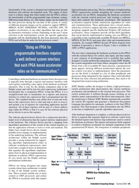
standards. An example MPEG4 decoder IP block diagram from<br />
Amphion Corporation is shown in Figure 3 that is available for<br />
ASIC or FPGA applications.<br />
The next step is integrating the hardware accelerator in the FPGA<br />
with the external busses for control, data input, and data output.<br />
A new category of development tool is available that enable<br />
designers to easily perform this integration. Using SOPC Builder,<br />
the system integration tool from Altera, designers select the IP<br />
blocks from a list of available IP. Upon selection, a parameterized<br />
menu appears showing different architectural options the user<br />
has control over prior to implementation. Once the parameters<br />
are set, the block is included in a list of other peripherals and<br />
processors being integrated by the engineer. Once each individual<br />
IP block has been selected and parameterized, they need to be<br />
integrated into an processing architecture.<br />
SOPC Builder enables the designer to define a high-performance<br />
switch architecture that interconnects the various hardware<br />
accelerators and peripherals to the external host processor. This<br />
switch architecture is defined through mouse clicking on an<br />
intuitive matrix representation of the block interconnection. Once<br />
the architecture is defined, SOPC Builder automatically assembles<br />
the various IPs together and generates a Hardware Description<br />
Language description for automatic synthesis to the final FPGA<br />
program. This final program is then downloaded onto the FPGA<br />
at run-time to implement a specific algorithm coprocessor.<br />
After hardware integration is complete, a software physical device<br />
driver is required that separates high-level software control from<br />
the detailed register and memory map architecture used to control<br />
the hardware accelerator. The register and memory fields required<br />
to control a hardware accelerator are standard components of the<br />
parameterized IP blocks. The integration of multiple peripherals<br />
FPGAs are being designed into many<br />
systems whose basic architecture is similar<br />
to that of the Delphi system architecture.<br />
These systems include one or more<br />
control or DSP processors and utilize<br />
the FPGA to accelerate tasks that require Figure 3<br />
<strong>Embedded</strong> <strong>Computing</strong> <strong>Design</strong> Summer 2004 / 45