Embedded Computing Design - OpenSystems Media
Embedded Computing Design - OpenSystems Media
Embedded Computing Design - OpenSystems Media
Create successful ePaper yourself
Turn your PDF publications into a flip-book with our unique Google optimized e-Paper software.
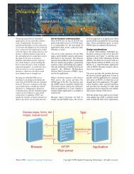
The Amanda companion chip in the Delphi architecture (see<br />
Figures 1, 2) uses two processing buses, the Pixel Bus for<br />
high-performance dataflows such as video processing, and the<br />
Register Bus for control applications. Each bus connects to the<br />
SH-4 MPX bus and an external memory interface. This combination<br />
of buses and memory interfaces provide the perfect interface<br />
to support a flexible video codec and wireless communications<br />
platform based on an FPGA coprocessor.<br />
Figure 1<br />
Figure 2<br />
FPGA coprocessing enables tight integration with a control<br />
or DSP processor to offload major algorithmic processing, while<br />
keeping a standard programming interface resident on the control<br />
processor. The integration works best when the primary dataflow<br />
of an algorithm stays on the FPGA or related memories. The<br />
algorithm is controlled by a much slower control signal from the<br />
control processor.<br />
This type of architecture can be applied to wireless communications<br />
to support the digital processing in GSM/EDGE, WCDMA,<br />
1xEVDO, and the different permutations of 802.11 with a single<br />
FPGA. The alternative is a unique hardware design for each standard<br />
thus multiplying costs and board area.<br />
In addition, FPGA coprocessing, applied to image processing,<br />
can enable support of multiple video codecs including MPEG2,<br />
MPEG4, and H.264 with a single FPGA. In fact, it can utilize the<br />
same FPGA as that used for the wireless communications.<br />
An FPGA coprocessor integrates with a processor based system<br />
through Direct Memory Access (DMA)-based interfaces. The<br />
software layer on the embedded processor includes an application<br />
interface for each coprocessor that includes<br />
an initialization routine that loads<br />
the FPGA with the appropriate application<br />
coprocessor. Once the application<br />
is initialized, software calls to the coprocessor<br />
control parameters, timing,<br />
and the flow of data into and out of the<br />
coprocessor. Depending on the standard<br />
being implemented, there may be a high<br />
level of interaction between the FPGA<br />
coprocessor and the control processor, or<br />
the FPGA coprocessor may be completely<br />
self-contained. In such cases the control<br />
processor simply loads the algorithm and<br />
gets out of the way.<br />
Each program image loaded onto the<br />
FPGA needs to integrate into the<br />
surrounding system. Using an FPGA<br />
for programmable functions requires a<br />
well defined system interface that each<br />
FPGA-based accelerator relies on for<br />
communication. In general, the FPGA<br />
will have multiple interfaces that connect<br />
to a control processor, memory, and<br />
other external peripherals or connectors.<br />
The FPGA may also contain several<br />
coprocessors simultaneously that all share<br />
a single interface to the control processor.<br />
Each peripheral or coprocessor can have<br />
additional buses for high-performance<br />
dataflow processing.<br />
In the case of a video codec, there will be<br />
an input source and an output destination.<br />
The video input interface in the Delphi<br />
system architecture is part of the Amanda<br />
companion ASIC and utilizes the ITU-R<br />
BT.656 interface for streaming video. This<br />
can be post-scaled and manipulated by<br />
the ASIC to fit a variety of different display<br />
panels. The FPGA will likely need to<br />
connect to two other buses, the memory<br />
bus on the companion chip and the<br />
PCI/MPX bus of the host control processor,<br />
which also connects to the<br />
companion chip. Through these three connections, the FPGA<br />
can support video and communications applications with<br />
high-bandwidth communication through the memory interface<br />
and control communication through the PCI/MPX bus.<br />
The FPGA provides a reprogrammable platform for applicationspecific<br />
processing architectures that complements the host<br />
processor. The FPGA program, however, is fundamentally<br />
different from that of a standard processor architecture. An FPGA<br />
provides a high-performance hardware fabric with programmable<br />
logic elements, routing, DSP processing blocks, memory, and<br />
I/O. The system architecture of an FPGA is executed in much the<br />
same manner as that for a standard ASSP where the dedicated<br />
44 / Summer 2004 <strong>Embedded</strong> <strong>Computing</strong> <strong>Design</strong>


