Embedded Computing Design - OpenSystems Media
Embedded Computing Design - OpenSystems Media
Embedded Computing Design - OpenSystems Media

Create successful ePaper yourself
Turn your PDF publications into a flip-book with our unique Google optimized e-Paper software.
field-proven, since it is unlikely that extra space will be needed<br />
to fix bugs within them. <strong>Design</strong>ers can also create hierarchical<br />
blocks that make efficient use of fixed resources such as RAM<br />
and multipliers.<br />
<strong>Design</strong> workflow<br />
Like ASIC designers, FPGA designers can accelerate design time<br />
by working as a team, and by reusing intellectual property from<br />
previous designs. Using ASIC-style design techniques enables<br />
teamwork and IP reuse. <strong>Design</strong>ers can take a block-based approach<br />
to divide their work into more manageable pieces, and assign<br />
responsibilities of designing them to individual team members.<br />
<strong>Design</strong>ers can also reuse blocks from previous designs, or even<br />
purchase them from a third party to save design and verification<br />
time.<br />
By employing ASIC-style techniques, designers can fully<br />
characterize their design blocks by freezing the placement within<br />
them so that power, timing, and other characteristics remain<br />
constant wherever they are used. They know that these blocks meet<br />
their physical requirements, and they can connect them to form<br />
larger designs that also meet their requirements.<br />
An example<br />
One challenge when designing with today’s complex FPGAs is that<br />
they have a limited amount of internal memory, and moving data<br />
to and from external memory frequently becomes a bottleneck. It<br />
would save a significant amount of time if FPGA designers could<br />
reuse standard high-speed memory interface blocks, with consistent<br />
performance, from one design to another.<br />
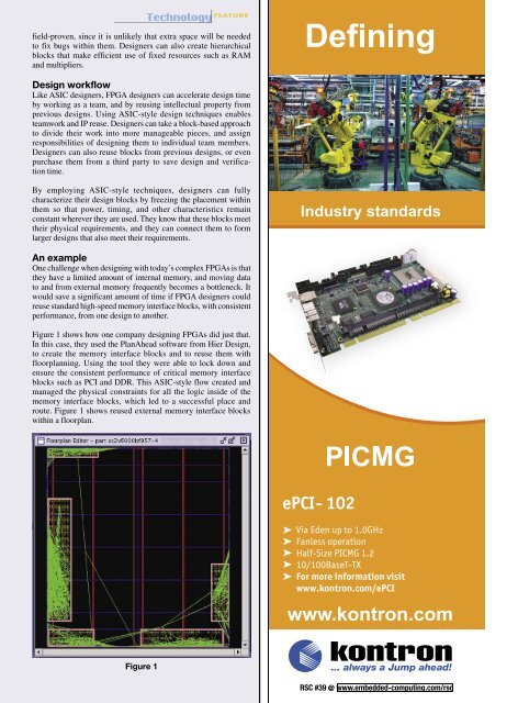
Figure 1 shows how one company designing FPGAs did just that.<br />
In this case, they used the PlanAhead software from Hier <strong>Design</strong>,<br />
to create the memory interface blocks and to reuse them with<br />
floorplanning. Using the tool they were able to lock down and<br />
ensure the consistent performance of critical memory interface<br />
blocks such as PCI and DDR. This ASIC-style flow created and<br />
managed the physical constraints for all the logic inside of the<br />
memory interface blocks, which led to a successful place and<br />
route. Figure 1 shows reused external memory interface blocks<br />
within a floorplan.<br />
Figure 1<br />
RSC #39 @ www.embedded-computing.com/rsc<br />
<strong>Embedded</strong> <strong>Computing</strong> <strong>Design</strong> Summer 2004 / 39