Create successful ePaper yourself
Turn your PDF publications into a flip-book with our unique Google optimized e-Paper software.
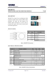
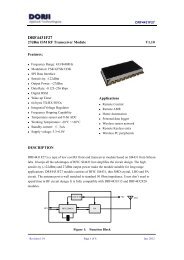
<strong>DRF1212D10N</strong><strong>DRF1212D10N</strong>10dBm Mesh Network Node Module V1.02Features• FSK Network Node Module• 433Mhz ISM frequency band• 5K bps FSK data rate• Multiple channels• 10dBm Max. output power• Baud rate configurable• Net ID configurable• Standby current < 1.5uA• Supply voltage 2.1~3.6VApplication• Home automation• Automatic meter reading• Wireless data logger• Wireless sensor networkDESCRIPTION<strong>DRF1212D10N</strong> is a low-cost sub-1 GHz transceiver module designed for operations in theunlicensed ISM (Industrial Scientific Medical) and LPRD bands. FSK (Frequency Shift Keying)modulation/demodulation, multi-channel operation, high bandwidth efficiency and anti-blockingperformance make <strong>DRF1212D10N</strong> modules easy to realize the robust and reliable wireless link.The module can be configured to work in different channels and different Net ID which makemultiple networks coexist possibly. It adopts high efficient looped interleaving EDAC (ErrorDetection and correction) coding with coding gain up to 3dB which keeps in advance in errorcorrection and coding efficiency over normal FEC (Forward Error Correction) coding. Because ofits high reliability in correction, modules can filter error and fake information automatically andrealize truly transparent wireless link, which makes <strong>DRF1212D10N</strong> very suitable in the rigidcommunication environment.<strong>DRF1212D10N</strong> module adopts 4 bytes Node ID and 2 bytes Net ID. Under the commanding ofconcentrator module DRF1212D17C, the MNET network can support up to 1024 node moduleswith 6 levels of routing.Revision 1.02 Page 1 of6 Jan. 2011
PIN FUNCTIONS<strong>DRF1212D10N</strong>PIN Name Function Description1 SGND Ground Sensor ground2 TXD Output UART output, TTL level3 RXD Input UART input, TTL level; pull-up resistor:47K Ohm4 BATT Power Positive power supply5 BATT Power Connecting with Pin 4 internally6 GND Ground Ground (0V)Table 1 <strong>DRF1212D10N</strong> Pin functionsELECTRICAL SPECIFICATIONSSymbol Parameter (condition) Min. Typ. Max. UnitsVCC Supply Voltage 2.1 3.6 VTemp Operating temperature range -20 25 70 °CRH Operating relative humidity 10 90 %Freq Frequency range 430 437 MHzFDEV Modulation deviation 67 KHzMod Modulation type FSKIDDReceive mode @1K bpsTransmit mode @5K bpsReceive mode @ pollingSleep mode2.835151.5mAmAuAuAPout Output power 10 dBmSen Receiving sensitivity @5K bps -107 dBmDRIN UART data rate 1.2 57.6 KbpsTw Wake-up time @5K bps 5 msTS Switching time 20 usCHBW Channel spacing 200 KHzZANT Antenna Impedance 50 OhmTable 2 <strong>DRF1212D10N</strong> Electrical SpecificationsABSOLUTE MAXIMUM RATINGSSymbol Parameter Min. Max. UnitsVCC Supply Voltage -0.3 3.7 VVI Input voltage -0.3 VCC+0.3 VRevision 1.02 Page 2 of6 Jan. 2011
<strong>DRF1212D10N</strong>VO Output voltage -0.3 VCC+0.3 VTST Storage temperature -55 125 °CTable 3 <strong>DRF1212D10N</strong> Maximum RatingsAPPLICATION INFORMATION1. Coding FormatPREAMBLE SYNCWORD ID DATA+FEC+CRCTable 4 <strong>DRF1212D10N</strong> Coding FormatThe preamble is alternative “1010” codes which is used to make the clock of receiversynchronous with transmitter. In normal conditions, 32 bits preamble is enough for use. When<strong>DRF1212D10N</strong> works in power-saving mode, the preamble also can be functioned to wake upthe receiver and it must be long enough in order to obtain such a function.If the receiver is configured to wake up at the interval of one second, it wakes up and searchesthe preamble (TW) every other second and lasting 16 bits. The transmitter must send preamblelonger than 1 second and then send synchronous word, which means the receiver can detectthe preamble and wake up receiver successfully.Figure 1: <strong>DRF1212D10N</strong> Timing Sequence2. Parameter SettingUsers can configure the parameters of <strong>DRF1212D10N</strong> modules by software tool. Theinterface of module is UART/TTL. If connecting it to PC, users need to use a TTL-to-RS232level converter to transform the levels. <strong>Dorji</strong> Applied Technologies also provides converterboard for configuration. Firstly users need to insert module into converter board and connectconverter board to PC, then open DORJI RF software. After that the status column of toolshould display “Found Device”. Users then can read/write the module. For more details,please check the operation manuals of converter boards on accessory page.Revision 1.02 Page 3 of6 Jan. 2011
<strong>DRF1212D10N</strong>Figure 2: DORJI RF TOOL3. ApplicationsThe connection diagram between <strong>DRF1212D10N</strong> and terminal equipment is showed as below.The Pin 4 and Pin 5 are connected together internally. In normal status the Pin 1 (SGND) is inhigh level. When DRF1212D12N receive the command from concentrator module, the SGNDwill be in low level. Since the SGND pin can accept 20mA drive-in current, users can takeadvantage of it by connecting the positive port of Optical module to BATT and negative portof it to SGND pin. When receiving read command, the SGND pin will be at low level, theOptical module begins to work and sends data through its TXD pin to <strong>DRF1212D10N</strong> module.The <strong>DRF1212D10N</strong> will add the value of present battery voltage in the last byte of datapackage and send it back to concentrator module.Figure 3: <strong>DRF1212D10N</strong> with Optical ModuleRevision 1.02 Page 4 of6 Jan. 2011
<strong>DRF1212D10N</strong><strong>DRF1212D10N</strong> integrates 12-bit high resolution AD converter so the Pin 1 (RXD) can be used asAD sampling to measure temperature or other analogue parameters.Figure 3: <strong>DRF1212D10N</strong> with Sensor ModuleMechanical DataFigure 5: Mechanical DataRevision 1.02 Page 5 of6 Jan. 2011
Ordering Information<strong>DRF1212D10N</strong>DRF 1212 D 10 N — 043 D1 2 3 4 5 6 7Num Symbol Meaning1 Category RF FSK module2 IC Type SX12123 Module Type Data transmission4 Power 10dBm output power5 Module Function Network node module6 Frequency Band 043: 433MHz7 Package DIP packageTable 5 Ordering information<strong>Dorji</strong> Applied TechnologiesA division of <strong>Dorji</strong> Industrial Group Co., LtdAdd.: Xinchenhuayuan 2, Dalangnanlu, Longhua,Baoan district, Shenzhen, China 518109Tel: 0086-755-28156122Fax.: 0086-755-28156133Email: sales@dorji.comWeb: http://www.dorji.com<strong>Dorji</strong> Industrial Group Co., Ltd reserves the right tomake corrections, modifications, improvements andother changes to its products and services at any timeand to discontinue any product or service withoutnotice. Customers are expected to visit websites forgetting newest product information before placingorders.These products are not designed for use in life supportappliances, devices or other products wheremalfunction of these products might result in personalinjury. Customers using these products in suchapplications do so at their own risk and agree to fullyindemnify <strong>Dorji</strong> Industrial Group for any damagesresulting from improper use.Revision 1.02 Page 6 of6 Jan. 2011