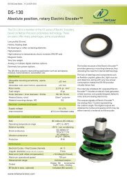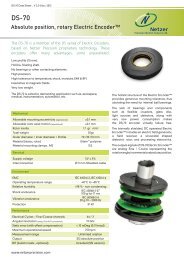
2790500 R/D converter with A/B incremental encoder output
2790500 R/D converter with A/B incremental encoder output
2790500 R/D converter with A/B incremental encoder output
- No tags were found...

You also want an ePaper? Increase the reach of your titles
YUMPU automatically turns print PDFs into web optimized ePapers that Google loves.
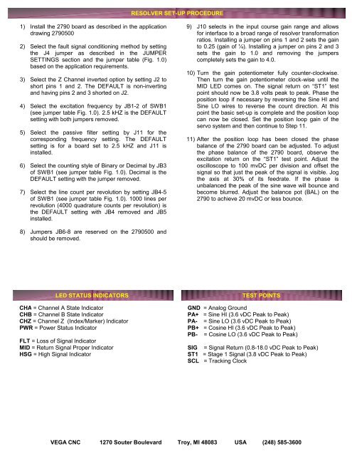
RESOLVER SET-UP PROCEDURE1) Install the 2790 board as described in the applicationdrawing <strong>2790500</strong>2) Select the fault signal conditioning method by settingthe J4 jumper as described in the JUMPERSETTINGS section and the jumper table (Fig. 1.0)based on the application requirements.3) Select the Z Channel inverted option by setting J2 toshort pins 1 and 2. The DEFAULT is non-invertingand having pins 2 and 3 shorted on J2.4) Select the excitation frequency by JB1-2 of SWB1(see jumper table Fig. 1.0). 2.5 kHZ is the DEFAULTsetting <strong>with</strong> both jumpers removed.5) Select the passive filter setting by J11 for thecorresponding frequency setting. The DEFAULTsetting is for a board set to 2.5 kHZ and J11 isinstalled.6) Select the counting style of Binary or Decimal by JB3of SWB1 (see jumper table Fig. 1.0). Decimal is theDEFAULT setting <strong>with</strong> the jumper removed.7) Select the line count per revolution by setting JB4-5of SWB1 (see jumper table Fig. 1.0). 1000 lines perrevolution (4000 quadrature counts per revolution) isthe DEFAULT setting <strong>with</strong> JB4 removed and JB5installed.9) J10 selects in the input course gain range and allowsfor interface to a broad range of resolver transformationratios. Installing a jumper on pins 1 and 2 sets the gainto 0.25 (gain of ¼). Installing a jumper on pins 2 and 3sets the gain to 1.0 and removing the jumperscompletely sets the gain to 4.0.10) Turn the gain potentiometer fully counter-clockwise.Then turn the gain potentiometer clock-wise until theMID LED comes on. The signal return on “ST1” testpoint should now be 3.8 volts peak to peak. Phase theposition loop if necessary by reversing the Sine HI andSine LO wires to reverse the count direction. At thispoint the basic set-up is complete and the position loopcan now be closed. Set the position loop gain of theservo system and then continue to Step 11.11) After the position loop has been closed the phasebalance of the 2790 board can be adjusted. To adjustthe phase balance of the 2790 board, observe theexcitation return on the “ST1” test point. Adjust theoscilloscope to 100 mvDC per division and offset thesignal so that just the peak of the signal is visible. Jogthe axis at 30% of its feedrate. If the phase isunbalanced the peak of the sine wave will bounce andbecome blurred. Adjust the balance pot (BAL) on the2790 to achieve 20 mvDC or less bounce.8) Jumpers JB6-8 are reserved on the <strong>2790500</strong> andshould be removed.LED STATUS INDICATORSCHA = Channel A State IndicatorCHB = Channel B State IndicatorCHZ = Channel Z (Index/Marker) IndicatorPWR = Power Status IndicatorFLT = Loss of Signal IndicatorMID = Return Signal Proper IndicatorHSG = High Signal IndicatorTEST POINTSGND = Analog GroundPA+ = Sine HI (3.6 vDC Peak to Peak)PA- = Sine LO (3.6 vDC Peak to Peak)PB+ = Cosine HI (3.6 vDC Peak to Peak)PB- = Cosine LO (3.6 vDC Peak to Peak)SIG = Signal Return (0.8-18.0 vDC Peak to Peak)ST1 = Stage 1 Signal (3.8 vDC Peak to Peak)SCL = Tracking ClockVEGA CNC 1270 Souter Boulevard Troy, MI 48083 USA (248) 585-3600