RND DC-DC Converter Series Data Sheet - Power-One
RND DC-DC Converter Series Data Sheet - Power-One
RND DC-DC Converter Series Data Sheet - Power-One

You also want an ePaper? Increase the reach of your titles
YUMPU automatically turns print PDFs into web optimized ePapers that Google loves.
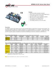
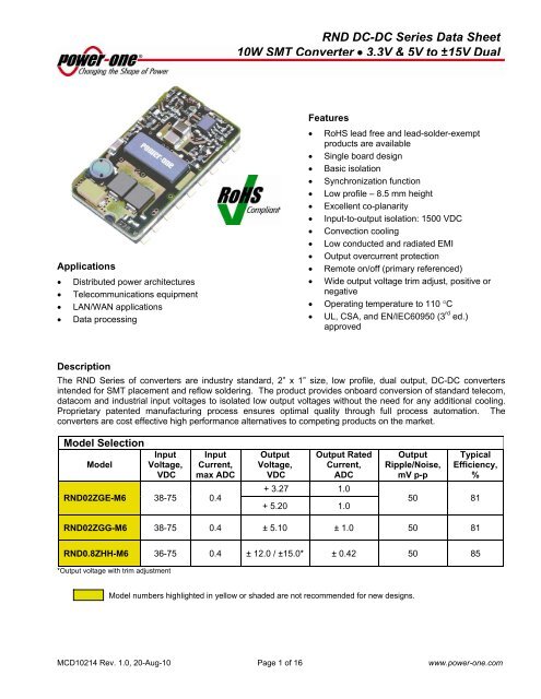
<strong>RND</strong> <strong>DC</strong>-<strong>DC</strong> <strong>Series</strong> <strong>Data</strong> <strong>Sheet</strong>10W SMT <strong>Converter</strong> 3.3V & 5V to ±15V DualFeaturesApplications Distributed power architectures Telecommunications equipment LAN/WAN applications <strong>Data</strong> processingRoHS lead free and lead-solder-exemptproducts are availableSingle board designBasic isolationSynchronization functionLow profile – 8.5 mm heightExcellent co-planarityInput-to-output isolation: 1500 V<strong>DC</strong>Convection coolingLow conducted and radiated EMIOutput overcurrent protectionRemote on/off (primary referenced)Wide output voltage trim adjust, positive ornegativeOperating temperature to 110 CUL, CSA, and EN/IEC60950 (3 rd ed.)approvedDescriptionThe <strong>RND</strong> <strong>Series</strong> of converters are industry standard, 2” x 1” size, low profile, dual output, <strong>DC</strong>-<strong>DC</strong> convertersintended for SMT placement and reflow soldering. The product provides onboard conversion of standard telecom,datacom and industrial input voltages to isolated low output voltages without the need for any additional cooling.Proprietary patented manufacturing process ensures optimal quality through full process automation. Theconverters are cost effective high performance alternatives to competing products on the market.Model SelectionModelInputVoltage,V<strong>DC</strong>InputCurrent,max A<strong>DC</strong><strong>RND</strong>02ZGE-M6 38-75 0.4OutputVoltage,V<strong>DC</strong>Output RatedCurrent,A<strong>DC</strong>+ 3.27 1.0+ 5.20 1.0OutputRipple/Noise,mV p-pTypicalEfficiency,%50 81<strong>RND</strong>02ZGG-M6 38-75 0.4 ± 5.10 ± 1.0 50 81<strong>RND</strong>0.8ZHH-M6 36-75 0.4 ± 12.0 / ±15.0* ± 0.42 50 85*Output voltage with trim adjustmentModel numbers highlighted in yellow or shaded are not recommended for new designs.MCD10214 Rev. 1.0, 20-Aug-10 Page 1 of 16 www.power-one.com
<strong>RND</strong> <strong>DC</strong>-<strong>DC</strong> <strong>Series</strong> <strong>Data</strong> <strong>Sheet</strong>10W SMT <strong>Converter</strong> 3.3V & 5V to ±15V DualAbsolute Maximum RatingsStresses in excess of the absolute maximum ratings may cause performance degradation, adversely affect longterm reliability and cause permanent damage to the converter. Specifications apply over specified input voltage,output load and temperature range, unless otherwise noted.Parameter Conditions/Description Min Max UnitsInput voltage (Vin)Transient Input Voltage (Vint)ContinuousTransient, 100 ms(36) 38 75100V<strong>DC</strong>V<strong>DC</strong>Operating CaseTemp. (Tc) All operating conditions -45 110 CStorage Temperature (Ts) -55 125 CON/OFF Control Voltage (Vrc) Referenced to -Vin -5 16 V<strong>DC</strong>Environmental and Mechanical SpecificationsParameter Conditions/Description Min Nom Max UnitsShock IEC68-2-27 100 gSinusoidal Vibration IEC68-2-6 10 gWeight 0.6/17 oz/gWater Washing Standard process YesMTBFPer Bellcore TR-NWT-000332(100% load @25 C, GB)4,132 kHrIsolation SpecificationsParameter Conditions/Description Min Nom Max UnitsInsulation Safety RatingBasicIsolation Voltage (Vps) 1,500 V<strong>DC</strong>Isolation Resistance (Rps) 10 MΩIsolation Capacitance (Cps) 2,200 pFInput SpecificationsParameter Conditions/Description Min Nom Max UnitsInput Voltage (Vin) Continuous 36 (38) 48 75 V<strong>DC</strong>Input Current when Shutdown Vin.Nom, Rem. Cont. activated 3 mA<strong>DC</strong>Input Current No Load Vin.Nom, Io = 0 10 mA<strong>DC</strong>Turn-On Input Voltage (-ZGG) Ramping Up, Io.Max 27.5 29 31.5Turn-Off Input Voltage (-ZGG) Ramping Down, Io.Max 26.5 28 30.5V<strong>DC</strong>Turn-On Input Voltage (-ZHH) Ramping Up, Io.Max 32 34.5 36Turn-Off Input Voltage (-ZHH) Ramping Down, Io.Max 30 33.5 35V<strong>DC</strong>Turn-On Input Voltage (-ZGE) Ramping Up, Io.Max 34 36.5 38V<strong>DC</strong>Turn-Off Input Voltage (-ZGE) Ramping Down, Io.Max 30 34.5 36Turn-On TimeTo Output Regulation BandAfter Remote ControlRise Time250255400 msmsmsInput Reflected Ripple Current Vin.Max, Io.Max 30 mAp-pInput Capacitance 1.4 FMCD10214 Rev. 1.0, 20-Aug-10 Page 2 of 16 www.power-one.com
<strong>RND</strong> <strong>DC</strong>-<strong>DC</strong> <strong>Series</strong> <strong>Data</strong> <strong>Sheet</strong>10W SMT <strong>Converter</strong> 3.3V & 5V to ±15V DualOutput SpecificationsAll specifications apply over input voltage, output load and temperature range, unless otherwise noted.<strong>RND</strong>02ZGE: (Vo1) 5.2V/1.0AParameter Conditions/Description Min Nom Max UnitsOutput VoltageVo Vin.Nom, Io1 = 0.6 A, Io2 =Setpoint Accuracy0.9 A, 25 C5.08 5.2 5.24 V<strong>DC</strong>Output Current * Io Vin.Min to Vin.Max 0.1 1.0 A<strong>DC</strong>Line Regulation Vin.Min to Vin.Max, 50%Io.Max50 mVLoad Regulation Vin.Nom, Io.Min to Io.Max 120 220 mVCross RegulationIo1 =1.0A, Io2 Min to Max,measure Vo1130 mVDynamic RegulationPeak DeviationSettling Time25-75% Io.Max load stepchange.to 1% error band200300± mVsOutput Voltage RippleVin.Min to Vin.Max, Io.Min toIo Max, 20 MHz Bandwidth50 100 mVp-pAdmissible Load Cap. Io.Max, Vin.Nom 2,200 FOutput Current LimitVout ≤0.90 Vo.Nom, bothThresholdoutputs set to Icl110 150 %Io.MaxSwitching Frequency Vin.Nom, Io.Max 380 kHzTemperature Coeff. 0.02 %Vo/CTrim RangeIo.Min to Io.Max, Vin.Min toVin.Max4.43 5.95 Vo<strong>RND</strong>02ZGE: (Vo2) 3.27V/1.0AParameter Conditions/Description Min Nom Max UnitsOutput VoltageVo Vin.Nom, Io1 = 0.6 A, Io2 =V<strong>DC</strong>3.24 3.27 3.3Setpoint Accuracy0.9 A, 25 COutput Current * Io Vin.Min to Vin.Max 0.1 1.0 A<strong>DC</strong>Line Regulation Vin.Min to Vin.Max, 50%mV40Io.MaxLoad Regulation Vin.Nom, Io.Min to Io.Max 100 210 mVCross RegulationIo2 =1.0A, Io1 Min to Max,mV90measure Vo2Dynamic RegulationPeak DeviationSettling Time25-75% Io.Max load stepchange.to 1% error band200300± mVsOutput Voltage RippleVin.Min to Vin.Max, Io.Min tomVp-p50 100Io Max, 20 MHz BandwidthAdmissible Load Cap. Io.Max, Vin.Nom 3,300 FOutput Current LimitVout ≤0.90 Vo.Nom, both%Io.Max110 150Thresholdoutputs set to IclSwitching Frequency Vin.Nom, Io.Max 380 kHzTemperature Coeff. 0.02 %Vo/CTrim RangeIo.Min to Io.Max, Vin.Min toVin.Max2.8 3.8 Vo* At Iout
<strong>RND</strong> <strong>DC</strong>-<strong>DC</strong> <strong>Series</strong> <strong>Data</strong> <strong>Sheet</strong>10W SMT <strong>Converter</strong> 3.3V & 5V to ±15V DualOutput SpecificationsAll specifications apply over input voltage, output load and temperature range, unless otherwise noted.Note:- Maximum output power is 9W<strong>RND</strong>02ZGG: (Vo1) +5.1V/0.75AParameter Conditions/Description Min Nom Max UnitsOutput VoltageVo Vin.Nom, Io1=Io2 = 0.3 A,Setpoint Accuracy25 C5.06 5.1 5.14 V<strong>DC</strong>Output Current * Io Vin.Min to Vin.Max 0.1 0.75 1.00 A<strong>DC</strong>Line Regulation Vin.Min to Vin.Max, 50%Io.Max40 mVLoad Regulation Vin.Nom, Io.Min to Io.Nom 100 250 mVCross RegulationIo1 = 0.5A, Io2 Min to Nom,measure Vo2100 mVDynamic RegulationPeak DeviationSettling Time25-75% Io.Max load stepchange.to 1% error band250200± mVsOutput Voltage RippleVin.Min to Vin.Max, Io.Min toIo Max, 20 MHz Bandwidth50 100 mVp-pAdmissible Load Cap. Io.Max, Vin.Nom 2,200 # FOutput Current LimitVout ≤0.90 Vo.Nom, bothThresholdoutputs set to Icl110 150 %Io.MaxSwitching Frequency Vin.Nom, Io.Max 400 kHzTemperature Coeff. 0.02 %Vo/CTrim RangeIo.Min to Io.Max, Vin.Min toVin.Max4.0 7.0 Vo<strong>RND</strong>02ZGG: (Vo2) -5.1V/0.75AParameter Conditions/Description Min Nom Max UnitsOutput VoltageVo Vin.Nom, Io1 =Io2 = 0.3 A,V<strong>DC</strong>-5.06 -5.10 -5.14Setpoint Accuracy25 COutput Current * Io Vin.Min to Vin.Max 0.1 0.75 1.0 A<strong>DC</strong>Line Regulation Vin.Min to Vin.Max, 50%mV40Io.MaxLoad Regulation Vin.Nom, Io.Min to Io.Nom 100 250 mVCross RegulationIo2 = 0.5 A, Io1 Min to Max,mV100measure Vo1Dynamic RegulationPeak DeviationSettling Time25-75% Io.Max load stepchange.to 1% error band250200± mVsOutput Voltage RippleVin.Min to Vin.Max, Io.Min tomVp-p50 100Io Max, 20 MHz BandwidthAdmissible Load Cap. Io.Max, Vin.Nom 2,200 # FOutput Current LimitVout ≤0.90 Vo.Nom, both%Io.Max110 150Thresholdoutputs set to IclSwitching Frequency Vin.Nom, Io.Max 400 kHzTemperature Coeff. 0.02 %Vo/CTrim RangeIo.Min to Io.Max, Vin.Min toVin.Max-4.0 -7.0 Vo* At Iout
<strong>RND</strong> <strong>DC</strong>-<strong>DC</strong> <strong>Series</strong> <strong>Data</strong> <strong>Sheet</strong>10W SMT <strong>Converter</strong> 3.3V & 5V to ±15V Dual<strong>RND</strong>02ZGG Typical Characteristic CurvesOutput Vo1 Vs LoadOuput Vo2 Vs Load7.07.06.06.0Output Voltage (V)5.04.03.02.01.0Vin MinVin NomVin MaxOutput Voltage (V)5.04.03.02.01.0Vin MinVin NomVin Max0.00.0 0.1 0.3 0.5 0.8 1.0 1.2 1.4 1.6 1.8 2.0Output Current (A)0.00.0 0.1 0.3 0.5 0.8 1.0 1.2 1.4 1.6 1.8 2.0Output Current (A)EfficiencyEfficiency Vs Load100%90%80%70%60%50%40%30%Vin MinVin Nom20%Vin Max10%0%0 Imin 25% Inom 50% Inom 75% Inom InomIout (A)MCD10214 Rev. 1.0, 20-Aug-10 Page 6 of 16 www.power-one.com
<strong>RND</strong> <strong>DC</strong>-<strong>DC</strong> <strong>Series</strong> <strong>Data</strong> <strong>Sheet</strong>10W SMT <strong>Converter</strong> 3.3V & 5V to ±15V DualOutput SpecificationsAll specifications apply over input voltage, output load and temperature range, unless otherwise noted.<strong>RND</strong>0.8ZHH: (Vo1) +12.0V/0.42AParameter Conditions/Description Min Nom Max UnitsOutput VoltageVoSetpoint AccuracyVin.Nom, Io = 0.3 A, 25 C11.82 12.00 12.18 V<strong>DC</strong>Output Current * Io Vin.Min to Vin.Max 0.042 0.42 A<strong>DC</strong>Line Regulation Vin.Min to Vin.Max, 50%Io.Max90 mVLoad Regulation Vin.Nom, Io.Min to Io.Max 100 170 mVCross RegulationIo1 = 0.42 A, Io2 Min to Max,measure Vo260 mVDynamic RegulationPeak DeviationSettling Time25-75% Io.Max load stepchange.to 1% error band400300± mVsOutput Voltage RippleVin.Min to Vin.Max, Io.Min toIo Max, 20 MHz Bandwidth40 100 mVp-pAdmissible Load Cap. Io.Max, Vin.Nom 100** FOutput Current LimitVout ≤0.90 Vo.Nom, bothThresholdoutputs set to Icl110 150 %Io.MaxSwitching Frequency Vin.Nom, Io.Max 400 kHzTemperature Coeff. 0.02 %Vo/CTrim RangeIo.Min to Io.Max, Vin.Min toVin.Max9.0 15.0 Vo<strong>RND</strong>0.8ZHH: (Vo2) -12.0V/0.42AParameter Conditions/Description Min Nom Max UnitsOutput VoltageVoSetpoint AccuracyVin.Nom, Io = 0.3 A, 25 C-11.82 -12.00 -12.18 V<strong>DC</strong>Output Current * Io Vin.Min to Vin.Max 0.042 0.42 A<strong>DC</strong>Line Regulation Vin.Min to Vin.Max, 50%Io.Max90 mVLoad Regulation Vin.Nom, Io.Min to Io.Max 100 170 mVCross RegulationIo1 = 0.42A, Io2 Min to Max,measure Vo260 mVDynamic RegulationPeak DeviationSettling Time25-75% Io.Max load stepchange.to 1% error band400300± mVsOutput Voltage RippleVin.Min to Vin.Max, Io.Min toIo Max, 20 MHz Bandwidth40 100 mVp-pAdmissible Load Cap. Io.Max, Vin.Nom 100** FOutput Current LimitVout ≤0.90 Vo.Nom, bothThresholdoutputs set to Icl110 150 %Io.MaxSwitching Frequency Vin.Nom, Io.Max 400 kHzTemperature Coeff. 0.02 %Vo/CTrim RangeIo.Min to Io.Max, Vin.Min toVin.Max-9.0 -15.0 Vo* At Iout
<strong>RND</strong> <strong>DC</strong>-<strong>DC</strong> <strong>Series</strong> <strong>Data</strong> <strong>Sheet</strong>10W SMT <strong>Converter</strong> 3.3V & 5V to ±15V Dual<strong>RND</strong>0.8ZHH Typical Characteristic Curves14Vo1 Vs Output Load14Vo2 Vs Output Load1212Output Voltage (V)108642Vin MinVin NomVin MaxOutput Voltage (V)108642Vin MinVin NomVin Max00.00 0.11 0.32 0.50 0.61 0.67Output Curremt (A)00.0 0.1 0.3 0.5 0.6 0.7Output Current (A)12.25Vo1 Cross Regulation12.15Vo2 Cross Regulation12.2012.10V01 Output Voltage (V)12.1512.1012.0512.0011.9511.9011.8511.8011.75Vin MinVin NomVin MaxV02 Output Voltage (V)12.0512.0011.9511.9011.8511.8011.75Vin MinVin NomVin Max11.70Imin 25% 50% 75% InomVo2 Output Curremt11.70Imin 25% 50% 75% InomVo1 Output CurremtEfficiency100%90%80%70%60%50%40%30%20%10%0%Efficiency Vs LoadVin MinVin NomVin Max0 Imin 25% Inom 50% Inom 75% Inom InomIout (A)MCD10214 Rev. 1.0, 20-Aug-10 Page 8 of 16 www.power-one.com
<strong>RND</strong> <strong>DC</strong>-<strong>DC</strong> <strong>Series</strong> <strong>Data</strong> <strong>Sheet</strong>10W SMT <strong>Converter</strong> 3.3V & 5V to ±15V DualFeature SpecificationsAll specifications apply over input voltage, output load and temperature range, unless otherwise noted.Parameter Conditions/Description Min Nom Max UnitsRemote Control:<strong>Converter</strong> OFF<strong>Converter</strong> ONSink CurrentRC pin is pulled lowVoltage source or open circuitVin=Vin.Nom-1.04.00.31.06V<strong>DC</strong>V<strong>DC</strong>mA<strong>DC</strong>[<strong>RND</strong>0.8ZHH model only]Synchronization:Frequency RangeTTL compatible square wave onsync pin. Referenced to -Vin450600kHzTemperature Derating CurvesThe derating curves below give an indication of the output power achievable with and without forced-air cooling.However in the final application, in order to ensure the reliability of the unit, care must be taken to ensure themaximum case temperature is not exceeded under any conditions.MCD10214 Rev. 1.0, 20-Aug-10 Page 9 of 16 www.power-one.com
<strong>RND</strong> <strong>DC</strong>-<strong>DC</strong> <strong>Series</strong> <strong>Data</strong> <strong>Sheet</strong>10W SMT <strong>Converter</strong> 3.3V & 5V to ±15V DualTypical ApplicationThis series of converters does not require anyexternal components for proper operation. However,if the distribution of the input voltage to the convertercontains significant inductance, a capacitor acrossthe input terminals may be required to stabilise theinput voltage. A minimum of 1 μF, quality electrolytic/ ceramic capacitor is recommended for this purpose.For output decoupling it is recommended to connect,directly across the output pins, a 1 μF ceramiccapacitor (for 3.3 V and 5 V outputs) or a 0.27 μFceramic capacitor (for 12 V outputs).KOhm2000150010005000<strong>RND</strong>0.8ZHH - Res istance require d todecrease Vion33.8 33.66 33.33 33 32 31Voltage (Vion)Synchronization FeatureIt is possible to synchronize the switching frequencyof one or more converters to an external symmetricalclock signal. It is recommended that the signal bedriven by a TTL compatible output. The rise time ofthe clock signal should be less than 10 ns. If thesynchronization feature is not used, it should be leftopen circuit.KOhm16 0 014 0 012 0 010 0 08006004002000<strong>RND</strong>0.8ZHH - Resistance required toincrease Vion34.3 34.8 35.2 37.5 40.5 42Voltage (Vion)Turn-On Input VoltageAn external resistor can program the input voltage atwhich the converter switches on. The voltage atwhich the unit switches off is typically 1 V below theturn-on input voltage (Vion).The characteristic curves below shows the typicalresistor values required to achieve adjustment ofturn-on input voltage (Vion).To decrease Vion the resistor should be connectedbetween pins 10 and 11.To increase Vion the resistor should be connectedbetween pins 11 and 17.KOhm16001400120010008006004002000<strong>RND</strong>02ZGE - Resistance required todecrease Vion35.6 35.4 35 34.2 33.5 33Voltage (Vion)<strong>RND</strong>02ZGE - Resistance required to increaseKOhmVion1600140012001000800600400200036.05 36.45 36.9 37.5 39.5 42Voltage (Vion)MCD10214 Rev. 1.0, 20-Aug-10 Page 10 of 16 www.power-one.com
<strong>RND</strong> <strong>DC</strong>-<strong>DC</strong> <strong>Series</strong> <strong>Data</strong> <strong>Sheet</strong>10W SMT <strong>Converter</strong> 3.3V & 5V to ±15V DualOutput Voltage TrimNote: For setting nominal output voltage pin 8 mustbe connected to pin 9.The trim feature allows the user to adjust the outputvoltage from the nominal. This can be used toaccommodate a different requirement or to doproduction margin testing.Output voltage can be adjusted by an externalresistor. If pin 8 and pin 9 are not connectedtogether the output will decrease to a low value. Toincrease Vo a resistor should be connected betweenpin 8 / 9 and pin 17 ( -Vin). To decrease Vo, aresistor should be connected between pin 8 and 9(NOR).To increase Vo:Radj = A x (B - Vd) / (Vd - Vo), kWhere: Vd = Desired output voltageVo = Nominal output voltage.To reduce Vo:Radj = C x (Vo - Vd) / (Vd - D), kWhere: Vd = Desired output voltageVo = Nominal output voltage.Model A B C D<strong>RND</strong>02ZGE 0.5 3.92 2.0 2.56<strong>RND</strong>02ZGG 0.5 7.1 2.243 3.7<strong>RND</strong>0.8ZHH 0.572 16.126 2.243 8.295Notes:1. When the output voltage is trimmed up, theoutput power from the converter must notexceed its maximum rating. This is determinedby measuring the output voltage on the outputpins, and multiplying it by the output current.2. The trim feature allows the generation ofadditional standard voltages such as ±15 V fromthe ±12 V model.Output Current LimitingWhen the output is overloaded above the maximumoutput current rating, the voltage will start to reduceto maintain the output power to a safe level. In acondition of high overload or short-circuit where theoutput voltage is pulled below approximately 30% ofVo.Nom, the unit will enter a ‘Hiccup’ mode ofoperation. Under this condition the unit will attemptto restart, approximately every 100 ms until theoverload has cleared.Thermal ConsiderationsThe converter is designed for natural or forcedconvection cooling. The output power of theconverter is limited by the maximum casetemperature (Tc). To ensure reliable long termoperation of the converters, and to comply withsafety agency requirements, <strong>Power</strong>-<strong>One</strong> limitsmaximum allowable case temperature (Tc) to 110 °C(see Mechanical Drawings).Remote Control FeatureThe remote control pin functions as a normal softshutdown. It is referenced to the –Vin pin. Withpositive logic, when the remote control pin is pulledlow, the output is turned off and the unit goes into avery low input power mode.An open collector switch is recommended to controlthe voltage between the remote control pin and -Vinpin of the converter. The remote control pin is pulledup internally, so no external voltage source isrequired. The user should avoid connecting aresistor between the remote control pin and the +Vinpin.The user must take care to ensure that the pinreference for the control is connected close to -Vinpin. The control signal must not be referencedahead of EMI filtering, or remotely from the unit. Ifthe remote control pin is not used, it can be leftfloating.Parallel OperationParalleling of two converters is possible by directconnection of the output voltage terminal pins. Theload regulation characteristic is designed to facilitatecurrent sharing (typically ± 20%).MCD10214 Rev. 1.0, 20-Aug-10 Page 11 of 16 www.power-one.com
<strong>RND</strong> <strong>DC</strong>-<strong>DC</strong> <strong>Series</strong> <strong>Data</strong> <strong>Sheet</strong>10W SMT <strong>Converter</strong> 3.3V & 5V to ±15V DualSafety ConsiderationsThese converters feature 1500 V<strong>DC</strong> isolation frominput to output. The input-to-output resistance isgreater than 10MΩ. These converters are providedwith Basic Insulation between input and outputcircuits according to EN60950 / UL1950 /CSA60950-00. Nevertheless, if the system usingthe converter needs to receive safety agencyapproval, certain rules must be followed in thedesign of the system. In particular, all of thecreepage and clearance requirements of the end-usesafety requirements must be observed. Thesedocuments include UL60950, CSA60950-00 andEN60950, although specific applications may haveadditional requirements.In order for the output of the converter to beconsidered as SELV (Safety Extra Low Voltage) orTNV-1, according to EN60950 / UL1950 /CSA60950-00, one of the following requirementsmust be met in the system design: The converter has no internal fuse. An externalfuse must be provided to protect the system fromcatastrophic failure. A fuse with a rating notgreater than 2.0 A is recommended. The usercan select a lower rating fuse based upon theinrush transient and the maximum input current ofthe converter, which occurs at the minimum inputvoltage. Both input traces and the chassisground trace (if applicable) must be capable ofconducting a current of 1.5 times the value of thefuse without opening. The fuse must not beplaced in the grounded input line, if any. If the voltage source feeding the module is SELV,the output of the converter is considered SELVand may be grounded or ungrounded. The circuitry on the converter carry transients,which exceed the input voltage. Even if the inputvoltage is SELV (
<strong>RND</strong> <strong>DC</strong>-<strong>DC</strong> <strong>Series</strong> <strong>Data</strong> <strong>Sheet</strong>10W SMT <strong>Converter</strong> 3.3V & 5V to ±15V DualSurface Mount AssemblySoldering:The following instructions must be observed whensoldering the unit. Failure to observe theseinstructions may result in failure or significantdegradation of the module performance. <strong>Power</strong>-<strong>One</strong>will not honor any warranty claims arising from failureto observe these instructions.This product is approved for forced convection reflowsoldering only..300250200150100Max. temp. on pins 1 and 10 during reflowsoldering (deg C)Peak Temperature(See fig below)tpThe curves below define the maximum peak reflowtemperature permissible measured on Pins 1 and10 of the converter.The lead-frame is constructed for a hightemperature glass filled, UL94V0 flame retardant,diallyl ortho-phthalate moulding compoundcommonly used for packaging of electronicscomponents. It has passed NASA outgassing testsand is certified to MIL-M-14. The coefficient ofthermal expansion is equivalent to FR4.The gull wing leads are formed to ensure optimalsolder joint strength and structure. Furthermorethey facilitate visual inspection (manual orautomatic). The leads are formed from a 97% Cualloy plated with Cu and Sn 90. This material iscommonly used in the manufacture of integratedcircuits. It has good corrosion resistance andexhibits the nobility inherent to all high copperalloys. Unlike brasses, this material is essentiallyimmune to stress corrosion cracking. It also exhibitsexcellent solderability. It is readily wetted by soldersand performs well in standard solderability tests.(Dip of Class II or better).The product is manufactured with a patentedprocess, which is fully automated, and ‘in-line’. Thisensures that there is no contamination ormechanical stress on the lead-frame so that the coplanarity and solderability are maintained.The product is shipped in JEDEC trays to ensurepreservation of the co-planarity and enable fullyautomated assembly in the final application.5000Restriction curve above 215ºCPeak temp. at pins 1 and 10 (ºC)2452402352302252202152102052004080120160Pick & Place Assembly:200Time (s)10 20 30 40 50 60tp (s)The product is designed with a large flat area in thecenter of the top surface to serve as a pick up pointfor automated vacuum pick and place equipment.The ‘open board’ construction of the unit ensuresthat weight is kept to a minimum. However due to therelatively large size of the component, a large nozzle(> 8.0 mm, depending on vacuum pressure) isrecommended for picking and placing.The unit may also be automatically handled using‘odd-form’ placement equipment, with mechanicalgrippers. For this type of equipment the end edgesof the device, which have no leads and also featurethe greatest dimensional accuracy, should be usedas pick-up points.240190 – 450 s280320360400440MCD10214 Rev. 1.0, 20-Aug-10 Page 13 of 16 www.power-one.com
<strong>RND</strong> <strong>DC</strong>-<strong>DC</strong> <strong>Series</strong> <strong>Data</strong> <strong>Sheet</strong>10W SMT <strong>Converter</strong> 3.3V & 5V to ±15V DualMechanical DrawingNote:- mm[inches]Tolerances: -0.5-10 ±0.110-100 ±0.2MCD10214 Rev. 1.0, 20-Aug-10 Page 14 of 16 www.power-one.com
<strong>RND</strong> <strong>DC</strong>-<strong>DC</strong> <strong>Series</strong> <strong>Data</strong> <strong>Sheet</strong>10W SMT <strong>Converter</strong> 3.3V & 5V to ±15V Dual322.624.15 43.833.362.131512.19JEDEC TRAY12.19MCD10214 Rev. 1.0, 20-Aug-10 Page 15 of 16 www.power-one.com
<strong>RND</strong> <strong>DC</strong>-<strong>DC</strong> <strong>Series</strong> <strong>Data</strong> <strong>Sheet</strong>10W SMT <strong>Converter</strong> 3.3V & 5V to ±15V DualPinoutPin Designation Function Reference1 Vout1 Output voltage 1 (positive) Secondary2 Rtn Output voltage return Secondary3 Vout2 Output voltage 2 Secondary4 NC Not connected Secondary5 NC Not connected Secondary6 NC Not connected Primary7 Sync Synchronization input Primary8 Trim Output voltage adjustPrimaryNote: - To set nominal output voltage connect pins 8 and 9 together9 NOR Connection for nominal output voltage Primary10 TOA Turn-on/off input voltage adjust Primary11 RC Remote control. Pull low to turn unit off Primary12 NC Not connected Primary13 NC Not connected Primary14 NC Not connected Primary15 NC Not connected Primary16 NC Not connected Primary17 -Vin Negative input voltage Primary18 +Vin Positive input voltage PrimaryOrdering InformationOptionsSuffixes to add to part numberRoHS lead-solder exempt compliant 1 No RoHS suffix character requiredRoHS compliant for all six substances Add "G" as the last character of the part number.1The solder exemption refers to all the restricted materials except lead in solder.NUCLEAR AND MEDICAL APPLICATIONS - <strong>Power</strong>-<strong>One</strong> products are not designed, intended for use in, or authorized for use as criticalcomponents in life support systems, equipment used in hazardous environments, or nuclear control systems without the express writtenconsent of the respective divisional president of <strong>Power</strong>-<strong>One</strong>, Inc.TECHNICAL REVISIONS - The appearance of products, including safety agency certifications pictured on labels, may change depending onthe date manufactured. Specifications are subject to change without notice.MCD10214 Rev. 1.0, 20-Aug-10 Page 16 of 16 www.power-one.com