214-Pin Micro-DIMM-DDR2-SDRAM Modules MDIMM DDR2 ... - UBiio
214-Pin Micro-DIMM-DDR2-SDRAM Modules MDIMM DDR2 ... - UBiio
214-Pin Micro-DIMM-DDR2-SDRAM Modules MDIMM DDR2 ... - UBiio

You also want an ePaper? Increase the reach of your titles
YUMPU automatically turns print PDFs into web optimized ePapers that Google loves.
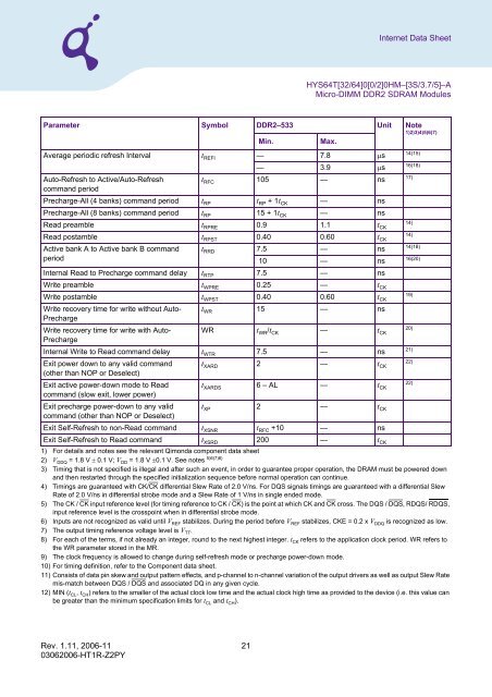
Internet Data SheetHYS64T[32/64]0[0/2]0HM–[3S/3.7/5]–A<strong>Micro</strong>-<strong>DIMM</strong> <strong>DDR2</strong> <strong>SDRAM</strong> <strong>Modules</strong>Parameter Symbol <strong>DDR2</strong>–533 Unit Note1)2)3)4)5)6)7)Min.Max.Average periodic refresh Interval t REFI — 7.8 µs14)15)— 3.9 µs16)18)Auto-Refresh to Active/Auto-Refreshcommand periodt RFC 105 — ns17)Precharge-All (4 banks) command period t RP t RP +1t CK — nsPrecharge-All (8 banks) command period t RP 15 + 1t CK — nsRead preamble t RPRE 0.9 1.1 t CK14)Read postamble t RPST 0.40 0.60 t CK14)Active bank A to Active bank B command t RRD 7.5 — nsperiod10 — nsInternal Read to Precharge command delay t RTP 7.5 — ns14)18)16)20)Write preamble t WPRE 0.25 — t CKWrite postamble t WPST 0.40 0.60 t CK19)Write recovery time for write without Auto-PrechargeWrite recovery time for write with Auto-Precharget WR 15 — nsWR t WR /t CK — t CK20)Internal Write to Read command delay t WTR 7.5 — ns21)Exit power down to any valid command(other than NOP or Deselect)Exit active power-down mode to Readcommand (slow exit, lower power)Exit precharge power-down to any validcommand (other than NOP or Deselect)t XARD 2 — t CK22)t XARDS 6 – AL — t CK22)t XP 2 — t CKExit Self-Refresh to non-Read command t XSNR t RFC +10 — nsExit Self-Refresh to Read command t XSRD 200 — t CK1) For details and notes see the relevant Qimonda component data sheet2) V DDQ = 1.8 V ± 0.1 V; V DD = 1.8 V ±0.1 V. See notes 5)6)7)8)3) Timing that is not specified is illegal and after such an event, in order to guarantee proper operation, the DRAM must be powered downand then restarted through the specified initialization sequence before normal operation can continue.4) Timings are guaranteed with CK/CK differential Slew Rate of 2.0 V/ns. For DQS signals timings are guaranteed with a differential SlewRate of 2.0 V/ns in differential strobe mode and a Slew Rate of 1 V/ns in single ended mode.5) The CK / CK input reference level (for timing reference to CK / CK) is the point at which CK and CK cross. The DQS / DQS, RDQS/ RDQS,input reference level is the crosspoint when in differential strobe mode.6) Inputs are not recognized as valid until V REF stabilizes. During the period before V REF stabilizes, CKE = 0.2 x V DDQ is recognized as low.7) The output timing reference voltage level is V TT .8) For each of the terms, if not already an integer, round to the next highest integer. t CK refers to the application clock period. WR refers tothe WR parameter stored in the MR.9) The clock frequency is allowed to change during self-refresh mode or precharge power-down mode.10) For timing definition, refer to the Component data sheet.11) Consists of data pin skew and output pattern effects, and p-channel to n-channel variation of the output drivers as well as output Slew Ratemis-match between DQS / DQS and associated DQ in any given cycle.12) MIN (t CL , t CH ) refers to the smaller of the actual clock low time and the actual clock high time as provided to the device (i.e. this value canbe greater than the minimum specification limits for t CL and t CH ).Rev. 1.11, 2006-11 2103062006-HT1R-Z2PY
![Internet Data Sheet HYB18TC256[80/16]0BF Rev. 1.3 - UBiio](https://img.yumpu.com/50510226/1/184x260/internet-data-sheet-hyb18tc25680-160bf-rev-13-ubiio.jpg?quality=85)
![Internet Data Sheet HYS72T[32/64]xxxHP-[3S/3.7]-A Rev. 1.01 - UBiio](https://img.yumpu.com/50510224/1/184x260/internet-data-sheet-hys72t32-64xxxhp-3s-37-a-rev-101-ubiio.jpg?quality=85)

![Internet Data Sheet HY[B/I]39SC128[800/160]FE Rev. 1.1 - UBiio](https://img.yumpu.com/31629373/1/184x260/internet-data-sheet-hyb-i39sc128800-160fe-rev-11-ubiio.jpg?quality=85)