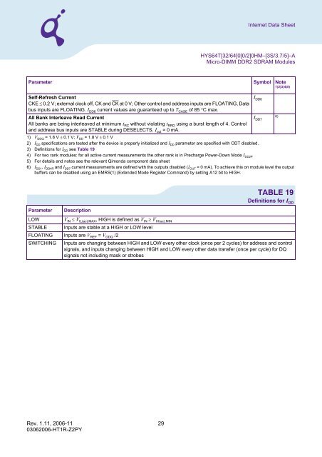
Internet Data SheetHYS64T[32/64]0[0/2]0HM–[3S/3.7/5]–A<strong>Micro</strong>-<strong>DIMM</strong> <strong>DDR2</strong> <strong>SDRAM</strong> <strong>Modules</strong>3.4 I DD Specifications and ConditionsThis chapter describes the I DD Specifications and Conditions.TABLE 18I DD Measurement ConditionsParameter Symbol Note1)2)3)4)5)Operating Current 0One bank Active - Precharge; t CK = t CK.MIN , t RC = t RC.MIN , t RAS = t RAS.MIN , CKE is HIGH, CS is HIGH betweenvalid commands. Address and control inputs are SWITCHING, Databus inputs are SWITCHING.Operating Current 1One bank Active - Read - Precharge; I OUT = 0 mA, BL = 4, t CK = t CK.MIN , t RC = t RC.MIN , t RAS = t RAS.MIN ,t RCD = t RCD.MIN , AL = 0, CL = CL MIN ; CKE is HIGH, CS is HIGH between valid commands. Address andcontrol inputs are SWITCHING, Databus inputs are SWITCHING.Precharge Standby CurrentAll banks idle; CS is HIGH; CKE is HIGH; t CK = t CK.MIN ; Other control and address inputs are SWITCHING,Databus inputs are SWITCHING.Precharge Power-Down CurrentOther control and address inputs are STABLE, Data bus inputs are FLOATING.Precharge Quiet Standby CurrentAll banks idle; CS is HIGH; CKE is HIGH; t CK = t CK.MIN ; Other control and address inputs are STABLE,Data bus inputs are FLOATING.Active Standby CurrentBurst Read: All banks open; Continuous burst reads; BL = 4; AL = 0, CL = CL MIN ; t CK = t CK.MIN ;t RAS = t RAS.MAX , t RP = t RP.MIN ; CKE is HIGH, CS is HIGH between valid commands. Address inputs areSWITCHING; Data Bus inputs are SWITCHING; I OUT = 0 mA.Active Power-Down CurrentAll banks open; t CK = t CK.MIN , CKE is LOW; Other control and address inputs are STABLE, Data bus inputsare FLOATING. MRS A12 bit is set to LOW (Fast Power-down Exit);Active Power-Down CurrentAll banks open; t CK = t CK.MIN , CKE is LOW; Other control and address inputs are STABLE, Data bus inputsare FLOATING. MRS A12 bit is set to HIGH (Slow Power-down Exit);Operating Current - Burst ReadAll banks open; Continuous burst reads; BL = 4; AL = 0, CL = CL MIN ; t CK = t CKMIN ; t RAS = t RASMAX ;t RP = t RPMIN ; CKE is HIGH, CS is HIGH between valid commands; Address inputs are SWITCHING; Databus inputs are SWITCHING; I OUT = 0mA.Operating Current - Burst WriteAll banks open; Continuous burst writes; BL = 4; AL = 0, CL = CL MIN ; t CK = t CK.MIN ;t RAS = t RAS.MAX. , t RP = t RP.MAX ; CKE is HIGH, CS is HIGH between valid commands. Address inputs areSWITCHING; Data Bus inputs are SWITCHING;Burst Refresh Currentt CK = t CK.MIN ., Refresh command every t RFC = t RFC.MIN interval, CKE is HIGH, CS is HIGH between validcommands, Other control and address inputs are SWITCHING, Data bus inputs are SWITCHING.Distributed Refresh Currentt CK = t CK.MIN. , Refresh command every t RFC = t REFI interval, CKE is LOW and CS is HIGH between validcommands, Other control and address inputs are SWITCHING, Data bus inputs are SWITCHING.I DD0I DD16)I DD2NI DD2PI DD2QI DD3NI DD3P(0)I DD3P(1)I DD4R6)I DD4WI DD5BI DD5DRev. 1.11, 2006-11 2803062006-HT1R-Z2PY
Internet Data SheetHYS64T[32/64]0[0/2]0HM–[3S/3.7/5]–A<strong>Micro</strong>-<strong>DIMM</strong> <strong>DDR2</strong> <strong>SDRAM</strong> <strong>Modules</strong>Parameter Symbol Note1)2)3)4)5)Self-Refresh CurrentCKE ≤ 0.2 V; external clock off, CK and CK at 0 V; Other control and address inputs are FLOATING, Databus inputs are FLOATING. I DD6 current values are guaranteed up to T CASE of 85 °C max.All Bank Interleave Read CurrentAll banks are being interleaved at minimum t RC without violating t RRD using a burst length of 4. Controland address bus inputs are STABLE during DESELECTS. I out = 0 mA.I DD6I DD76)1) V DDQ = 1.8 V ± 0.1 V; V DD = 1.8 V ± 0.1 V2) I DD specifications are tested after the device is properly initialized and I DD parameter are specified with ODT disabled.3) Definitions for I DD see Table 194) For two rank modules: for all active current measurements the other rank is in Precharge Power-Down Mode I DD2P5) For details and notes see the relevant Qimonda component data sheet6) I DD1 , I DD4R and I DD7 current measurements are defined with the outputs disabled (I OUT = 0 mA). To achieve this on module level the outputbuffers can be disabled using an EMRS(1) (Extended Mode Register Command) by setting A12 bit to HIGH.TABLE 19Definitions for I DDParameter DescriptionLOW V IN ≤ V IL(ac).MAX , HIGH is defined as V IN ≥ V IH(ac).MINSTABLE Inputs are stable at a HIGH or LOW levelFLOATING Inputs are V REF = V DDQ /2SWITCHING Inputs are changing between HIGH and LOW every other clock (once per 2 cycles) for address and controlsignals, and inputs changing between HIGH and LOW every other data transfer (once per cycle) for DQsignals not including mask or strobesRev. 1.11, 2006-11 2903062006-HT1R-Z2PY


![Internet Data Sheet HYB18TC256[80/16]0BF Rev. 1.3 - UBiio](https://img.yumpu.com/50510226/1/184x260/internet-data-sheet-hyb18tc25680-160bf-rev-13-ubiio.jpg?quality=85)
![Internet Data Sheet HYS72T[32/64]xxxHP-[3S/3.7]-A Rev. 1.01 - UBiio](https://img.yumpu.com/50510224/1/184x260/internet-data-sheet-hys72t32-64xxxhp-3s-37-a-rev-101-ubiio.jpg?quality=85)

![Internet Data Sheet HY[B/I]39SC128[800/160]FE Rev. 1.1 - UBiio](https://img.yumpu.com/31629373/1/184x260/internet-data-sheet-hyb-i39sc128800-160fe-rev-11-ubiio.jpg?quality=85)