214-Pin Micro-DIMM-DDR2-SDRAM Modules MDIMM DDR2 ... - UBiio
214-Pin Micro-DIMM-DDR2-SDRAM Modules MDIMM DDR2 ... - UBiio
214-Pin Micro-DIMM-DDR2-SDRAM Modules MDIMM DDR2 ... - UBiio

You also want an ePaper? Increase the reach of your titles
YUMPU automatically turns print PDFs into web optimized ePapers that Google loves.
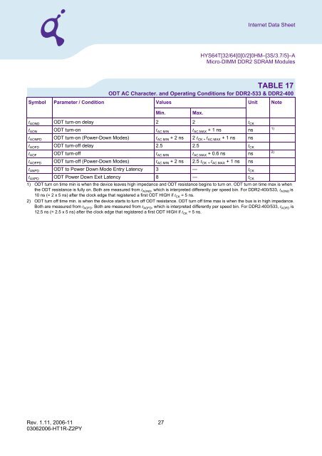
Internet Data SheetHYS64T[32/64]0[0/2]0HM–[3S/3.7/5]–A<strong>Micro</strong>-<strong>DIMM</strong> <strong>DDR2</strong> <strong>SDRAM</strong> <strong>Modules</strong>TABLE 17ODT AC Character. and Operating Conditions for <strong>DDR2</strong>-533 & <strong>DDR2</strong>-400Symbol Parameter / Condition Values Unit NoteMin.Max.t AOND ODT turn-on delay 2 2 t CKt AON ODT turn-on t AC.MIN t AC.MAX + 1 ns nst AONPD ODT turn-on (Power-Down Modes) t AC.MIN + 2 ns 2 t CK + t AC.MAX + 1 ns nst AOFD ODT turn-off delay 2.5 2.5 t CKt AOF ODT turn-off t AC.MIN t AC.MAX + 0.6 ns nst AOFPD ODT turn-off (Power-Down Modes) t AC.MIN + 2 ns 2.5 t CK + t AC.MAX + 1 ns ns1)2)t ANPD ODT to Power Down Mode Entry Latency 3 — t CKt AXPD ODT Power Down Exit Latency 8 — t CK1) ODT turn on time min is when the device leaves high impedance and ODT resistance begins to turn on. ODT turn on time max is whenthe ODT resistance is fully on. Both are measured from t AOND , which is interpreted differently per speed bin. For <strong>DDR2</strong>-400/533, t AOND is10 ns (= 2 x 5 ns) after the clock edge that registered a first ODT HIGH if t CK = 5 ns.2) ODT turn off time min. is when the device starts to turn off ODT resistance. ODT turn off time max is when the bus is in high impedance.Both are measured from t AOFD . Both are measured from t AOFD , which is interpreted differently per speed bin. For <strong>DDR2</strong>-400/533, t AOFD is12.5 ns (= 2.5 x 5 ns) after the clock edge that registered a first ODT HIGH if t CK = 5 ns.Rev. 1.11, 2006-11 2703062006-HT1R-Z2PY
![Internet Data Sheet HYB18TC256[80/16]0BF Rev. 1.3 - UBiio](https://img.yumpu.com/50510226/1/184x260/internet-data-sheet-hyb18tc25680-160bf-rev-13-ubiio.jpg?quality=85)
![Internet Data Sheet HYS72T[32/64]xxxHP-[3S/3.7]-A Rev. 1.01 - UBiio](https://img.yumpu.com/50510224/1/184x260/internet-data-sheet-hys72t32-64xxxhp-3s-37-a-rev-101-ubiio.jpg?quality=85)

![Internet Data Sheet HY[B/I]39SC128[800/160]FE Rev. 1.1 - UBiio](https://img.yumpu.com/31629373/1/184x260/internet-data-sheet-hyb-i39sc128800-160fe-rev-11-ubiio.jpg?quality=85)