

Discover New Applications For Low-Cost Solutions Discover ... - Xilinx
Discover New Applications For Low-Cost Solutions Discover ... - Xilinx
Discover New Applications For Low-Cost Solutions Discover ... - Xilinx

Create successful ePaper yourself
Turn your PDF publications into a flip-book with our unique Google optimized e-Paper software.
ISSUE 47, FALL 2003 XCELL JOURNAL XILINX, INC.<br />
Xcell Issue 47<br />
Fall 2003<br />
journal<br />
THE AUTHORITATIVE JOURNAL FOR PROGRAMMABLE LOGIC USERS<br />
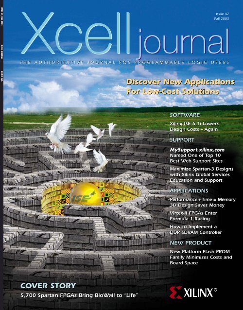
COVER STORY<br />
5,700 Spartan FPGAs Bring BioWall to “Life”<br />
<strong>Discover</strong> <strong>New</strong> <strong>Applications</strong><br />
<strong>For</strong> <strong>Low</strong>-<strong>Cost</strong> <strong>Solutions</strong><br />
SOFTWARE<br />
<strong>Xilinx</strong> ISE 6.1i <strong>Low</strong>ers<br />
Design <strong>Cost</strong>s – Again<br />
SUPPORT<br />
MySupport.xilinx.com<br />
Named One of Top 10<br />
Best Web Support Sites<br />
Maximize Spartan-3 Designs<br />
with <strong>Xilinx</strong> Global Services<br />
Education and Support<br />
APPLICATIONS<br />
Performance + Time = Memory<br />
3D Design Saves Money<br />
Virtex-II FPGAs Enter<br />
<strong>For</strong>mula 1 Racing<br />
How to Implement a<br />
DDR SDRAM Controller<br />
NEW PRODUCT<br />
<strong>New</strong> Platform Flash PROM<br />
Family Minimizes <strong>Cost</strong>s and<br />
Board Space<br />
R
Add Bluetooth to your<br />
MicroBlaze-based designs.<br />
(It doesn’t get any easier than this.)<br />
Now there’s a faster, easier way to build and test a Bluetooth ® system using<br />
embedded processors. It’s the Embedded Bluetooth Development Kit from<br />
Memec Design, and it provides everything you need to add a Bluetooth interface<br />
to existing <strong>Xilinx</strong>® MicroBlaze designs. Developed with industry-leading<br />
partners, this unique kit can help you save weeks of development time in your<br />
challenging next-generation applications. To find out more, contact us at<br />
www.insight.na.memec.com/xilinx_bluetooth.<br />
Americas, Europe, Asia, & Japan
EDITOR IN CHIEF Carlis Collins<br />
editor@xilinx.com<br />
408-879-4519<br />
MANAGING EDITOR Tom Durkin<br />
tom.durkin@xilinx.com<br />
530-271-0899<br />
ASSOCIATE EDITOR Jack Shandle<br />
COPY EDITOR Charmaine Cooper Hussain<br />
XCELL ONLINE EDITOR Tom Pyles<br />
tom.pyles@xilinx.com<br />
720-652-3883<br />
ADVERTISING SALES Dan Teie<br />
1-800-493-5551<br />
ART DIRECTOR Scott Blair<br />
Xcell journal<br />
<strong>Xilinx</strong>, Inc.<br />
2100 Logic Drive<br />
San Jose, CA 95124-3400<br />
Phone: 408-559-7778<br />
FAX: 408-879-4780<br />
©2003 <strong>Xilinx</strong>, Inc.<br />
All rights reserved.<br />
Xcell is published quarterly. XILINX, the <strong>Xilinx</strong> logo,<br />
CoolRunner, Rocket Chips, Rocket IP, Spartan, and<br />
Virtex are registered trademarks of <strong>Xilinx</strong>, Inc. ACE<br />
Controller, ACE Flash, Alliance Series, AllianceCORE,<br />
ChipScope, CORE Generator, Fast CONNECT, Fast FLASH,<br />
Fast Zero Power, Foundation, HDL Bencher, IRL, J Drive,<br />
LogiCORE, MicroBlaze, MultiLINX, NanoBlaze,<br />
PicoBlaze, QPro, Real-PCI, RocketIO, RocketPHY,<br />
SelectIO, SelectRAM, SelectRAM+, Smart-IP, System<br />
ACE, Virtex-II Pro, Virtex-II EasyPath, WebFITTER,<br />
WebPACK, WebPOWERED, XACT-Floorplanner, XACT-<br />
Performance, XAPP, XC designated products, <strong>Xilinx</strong><br />
Foundation Series, <strong>Xilinx</strong> XDTV, and XtremeDSP are<br />
trademarks, and The Programmable Logic Company is<br />
a service mark of <strong>Xilinx</strong>, Inc. Other brand or product<br />
names are registered trademarks or trademarks of<br />
their respective owners.<br />
The articles, information, and other materials included<br />
in this issue are provided solely for the convenience<br />
of our readers. <strong>Xilinx</strong> makes no warranties, express,<br />
implied, statutory, or otherwise, and accepts no liability<br />
with respect to any such articles, information, or<br />
other materials or their use, and any use thereof is<br />
solely at the risk of the user. Any person or entity<br />
using such information in any way releases and<br />
waives any claim it might have against <strong>Xilinx</strong> for any<br />
loss, damage, or expense caused thereby.<br />
L E T T E R F R O M T H E E D I T O R<br />
<strong>Xilinx</strong> Wins Again<br />
X<br />
ilinx has built its reputation on the triumvirate of silicon, software, and support.<br />
And although silicon and software get the most news coverage, it’s the support services<br />
team that holds it all together.<br />
The support.xilinx.com website – and the personalized mysupport.xilinx.com portals – are accessed<br />
by more than 110,000 users each month, and are credited for saving customers substantial time<br />
to knowledge, which translates to faster time to market.<br />
In fact, the MySupport.xilinx.com support service is so good that the<br />
Association of Support Professionals has named it to its list of “The Year’s<br />
Ten Best Web Support Sites.” <strong>Xilinx</strong> joins fellow industry leaders Dell,<br />
Hewlett Packard, Mentor Graphics, and Novell on the list of companies<br />
awarded for excellence in online service and support.<br />
To select this year’s winners, judges evaluated companies on such criteria as usability, design, navigation,<br />
and knowledge base, as well as search implementation, interactive features, personalization,<br />
and major site development.<br />
According to Jeffrey Tarter, executive director of the Association of Support Professionals, “Users<br />
are looking for highly interactive technical support services they can personalize to fit their needs<br />
and can access in real time. <strong>Xilinx</strong> is a leader in delivering the kind of online support customers<br />
are looking for.”<br />
Co-winner Mentor Graphics also praised MySupport.xilinx.com: “Many of our customers have told<br />
us that the quality and coverage of support.xilinx.com’s technical content allows them to readily<br />
understand complex FPGA architectures.”<br />
As we said, <strong>Xilinx</strong> support doesn’t get as much publicity as <strong>Xilinx</strong> silicon and software, but it is<br />
just as important.<br />
Don Mullikin, vice president of <strong>Xilinx</strong> Global Services, puts it this way: “Design teams tackling<br />
today’s most complex system-design challenges need support that matches the caliber of the technical<br />
capabilities of our products.”<br />
Our award-winning support matches our award-winning hardware and software, so you get a<br />
complete design solution that is the best in the industry.<br />
Tom Durkin<br />
Managing Editor<br />
Correction<br />
In the summer 2003 edition of Xcell Journal, the URL for more information on RocketPHY transceivers<br />
was incorrectly reported in the article “<strong>New</strong> RocketPHY Transceiver Family Debuts at 10 Gbps.” The correct<br />
URL is www.xilinx.com/rocketphy/. We regret this error and any inconvenience it may have caused.<br />
3
20<br />
F A L L 2 0 0 3, I S S U E 4 7<br />
Biology Goes Digital<br />
An array of 5,700 Spartan FPGAs brings the BioWall to “Life.”<br />
6<br />
COVER STORY<br />
Performance + Time = Memory<br />
By approaching FPGA designs as<br />
three-dimensional endeavors, you can<br />
radically reduce device size – and cost.<br />
ISE 6.1i Continues to<br />
<strong>Low</strong>er Design <strong>Cost</strong>s<br />
The latest release of <strong>Xilinx</strong><br />
programmable logic design software<br />
saves you time – and money<br />
<strong>For</strong>mula1 Racing: The <strong>Xilinx</strong> Advantage<br />
The BMW WilliamsF1 team lifts the hood on its<br />
fifth-generation vehicle control system<br />
46<br />
24<br />
Xcell Xcelljournal journal<br />
View from the Top................................................................5<br />
ISE 6.1i Continues to <strong>Low</strong>er Design <strong>Cost</strong>s ................................6<br />
Put Hardware in the Loop with System Generator for DSP..........8<br />
Get Physical with the Palace Synthesis Solution......................11<br />
Seamless Co-Verification Accelerates Time to Market ...............14<br />
In FPGA Synthesis, Timing Is Everything ................................18<br />
Advanced Switching Expands PCI Express...............................20<br />
Get the Platform Flash PROMise ...........................................23<br />
Performance + Time = Memory ...........................................24<br />
How to Implement a DDR SDRAM Controller ..........................30<br />
Is Your FPGA Design Secure? ...............................................32<br />
Virtex FPGAs Tame DSP-Hungry Designs.................................36<br />
Biology Goes Digital – The BioWall Story ..............................40<br />
<strong>For</strong>mula 1 Racing: The <strong>Xilinx</strong> Advantage................................46<br />
CoolRunner-II Has Hidden Talents..........................................50<br />
Boeing Uses Virtex-II Pro for Image Processing .......................53<br />
Explore the CoolRunner-II Design Kit......................................58<br />
Develop <strong>Applications</strong> Right Out of the Box..............................61<br />
Memec Design Simplifies Bluetooth Development ...................64<br />
Save Time, Money, and Space .............................................68<br />
Take the Titanium Solution ..................................................71<br />
Maximize Your Success with Spartan-3 Designs ......................72<br />
It’s a Programmable World ..................................................74<br />
<strong>Xilinx</strong> Partner Yellow Pages..................................................77<br />
Reference Pages.................................................................84<br />
To subscribe to the printed Xcell Journal,<br />
or to view the Web-based Xcell Online Journal, visit:<br />
www.xilinx.com/publications/xcellonline/
View<br />
from the top<br />
Innovation, Education, Exploration<br />
by Wim Roelandts<br />
CEO, <strong>Xilinx</strong>, Inc.<br />
<strong>Xilinx</strong> products<br />
and services continue<br />
to expand<br />
the limits of possibility.<br />
We strive to<br />
make the best and<br />
most innovative<br />
products in the<br />
programmable<br />
logic industry –<br />
and deliver them<br />
as a complete solution that gives you everything<br />
you need to bring your product to<br />
market first. Here are a few of our innovations<br />
that may interest you.<br />
Programmable World<br />
On May 6, <strong>Xilinx</strong> launched Programmable<br />
World 2003 – a nine-month international<br />
initiative designed to help you understand<br />
and use the latest programmable logic solutions.<br />
It includes technical forums, exhibits,<br />
and workshops in dozens of cities around the<br />
world. By the time it ends in November,<br />
Programmable World 2003 will have<br />
reached more than 10,000 executives, system<br />
architects, engineers, and project managers<br />
worldwide. Co-sponsored by more than 30<br />
industry leaders – including Agilent,<br />
Cadence, IBM, Intel, Texas Instruments,<br />
Mentor Graphics, and Wind River Systems –<br />
Programmable World 2003 started in North<br />
America, then went to Europe, on to China<br />
and Taiwan, and will finish in Japan and<br />
Korea in November.<br />
Following the worldwide forums, which<br />
ended in August, we have been holding indepth<br />
technical workshops, including multiple<br />
full-day courses on high-speed DSP,<br />
connectivity, processing, and system design.<br />
At the Programmable World 2003 forum<br />
in Japan this summer, Dr. Tsugio Makimoto,<br />
chief technical officer of Sony, asserted that<br />
field programmability is “hitting its peak”<br />
from 1997 through 2007. Dr. Makimoto<br />
stated a second wave of digital consumer<br />
From Programmable World in 2003 to landing on Mars in 2004,<br />
<strong>Xilinx</strong> leads the industry in new products and new applications.<br />
products will become the mainstay for<br />
future market expansion, just as personal<br />
computing products drove the first wave of<br />
the digital revolution. “Field programmability<br />
is a must in this new era of digital consumer<br />
goods,” Dr. Makimoto said. “These<br />
products have short time-to-market windows,<br />
and product life cycles that come<br />
quickly and end dramatically. Flexible, agile<br />
solutions are critical.”<br />
<strong>Xilinx</strong> Goes to Mars<br />
NASA recently launched two Mars<br />
Exploration Rover (MER) missions, which<br />
depend on the most advanced, radiationtolerant<br />
Virtex FPGAs in critical applications<br />
for both the landers and rover vehicles.<br />
The Spirit MER was launched June 10 and<br />
the Opportunity MER was launched July 7.<br />
Chosen because of their reprogrammability<br />
and high densities, the Virtex FPGAs<br />
serve as the main brain of the motor control<br />
boards. These FPGAs will be used to control<br />
the pyrotechnic devices that will cushion the<br />
touchdown of the landers in January 2004.<br />
The <strong>Xilinx</strong> FPGAs will also direct the motor<br />
control functions on the rovers, including<br />
controllers for the wheels, steering, and<br />
antenna gimbals.<br />
The radiation-tolerant Virtex devices on<br />
the two MER missions have up to one million<br />
system gates and total ionizing dose guaranteed<br />
to 100 kRads(si). We will soon announce<br />
a next-generation family of radiation-tolerant<br />
Virtex-II products with up to six million system<br />
gates and total ionizing dose guaranteed<br />
to 200 kRads(si).<br />
RocketPHY<br />
In May, we introduced our new RocketPHY<br />
stand-alone, SONET-compliant, 10 Gbps<br />
transceivers. These devices are among the<br />
industry’s first 10 Gbps products using CMOS<br />
process technology.<br />
The RocketPHY transceivers are the first<br />
products from <strong>Xilinx</strong> that are not directly<br />
related to programmable logic devices, but<br />
they are designed to work with our FPGAs.<br />
These transceivers use the same high-speed<br />
I/O technology as our Virtex-II Pro X<br />
FPGAs in application-specific designs that<br />
solve many I/O challenges – at far less cost<br />
than any competing product in networking<br />
applications.<br />
Conclusion<br />
<strong>Xilinx</strong> continues to innovate in technology<br />
and penetrate new markets. Although our<br />
process technology, devices, and software<br />
are continually setting the highest standards<br />
for performance, quality, and reliability, we<br />
are also setting new standards in other critical<br />
areas that affect your life. You’ll find that<br />
our products, our support services, and our<br />
educational programs work together to<br />
bring you a cohesive, faster time to market,<br />
and lowest cost path to your next product<br />
introduction. There simply is no easier,<br />
faster, or lower cost way to develop flexible<br />
new products than with <strong>Xilinx</strong> silicon, software,<br />
and support.<br />
6Fall 2003 Xcell Journal Xcell Journal Spring 2003 5
ISE 6.1i Continues to<br />
<strong>Low</strong>er Design <strong>Cost</strong>s<br />
The latest release of <strong>Xilinx</strong> programmable<br />
design software saves you time – and money.<br />
by Lee Hansen<br />
Product <strong>Solutions</strong> Marketing<br />
<strong>Xilinx</strong>, Inc.<br />
lee.hansen@xilinx.com<br />
The newest version of <strong>Xilinx</strong> Integrated<br />
Software Environment programmable<br />
design tools – ISE 6.1i – is now available<br />
to registered in-maintenance <strong>Xilinx</strong><br />
customers.<br />
This new release of our industryleading<br />
programmable design suite continues<br />
the <strong>Xilinx</strong> commitment to lower<br />
your design costs, to deliver ease of use<br />
that focuses on solving your specific<br />
engineering problems, and to expand<br />
support for low-cost Spartan-3<br />
FPGAs – and native support for the Red<br />
Hat Linux operating system.<br />
Some of the new capabilities in ISE<br />
6.1i include:<br />
• Support for the largest Spartan-3<br />
XC3S4000 and XC3S5000 devices<br />
• Increased Spartan-3 device support<br />
in ISE WebPACK and ISE BaseX<br />
• <strong>New</strong> ISE native Linux support<br />
• Automatic Web software update<br />
• PACE (Pinout and Area Constraints<br />
Editor) enhancements for CPLD,<br />
and PC board design assistance<br />
• Project Navigator mixed-language<br />
and embedded design enhancements<br />
• As much as 15% better performance<br />
than ISE 5.1i.<br />
ISE Shrinks <strong>Cost</strong>s<br />
Spartan-3 Platform FPGAs are the<br />
world’s lowest cost FPGA device family.<br />
ISE 6.1i software will help you lower the<br />
cost of using Spartan-3 FPGAs even further<br />
with these new features.<br />
More Spartan-3 Devices in ISE<br />
ISE WebPACK 6.1i, which is free to<br />
designers, has added support for the<br />
Spartan-3 XC3S200 and XC3S400<br />
devices, at 200,000 and 400,000 system<br />
gates, respectively. ISE BaseX now supports<br />
the XC3S400 device as well.<br />
6 Xcell Journal Fall 2003
High Density Spartan-3 Support<br />
ISE Foundation and ISE Alliance<br />
Series 6.1i versions support the<br />
highest-density Spartan-3 devices, the<br />
XC3S4000 and XC3S5000 FPGAs at 4<br />
million and 5 million gates, respectively.<br />
Now you have even greater flexibility in<br />
choosing Spartan-3 devices and<br />
ISE configurations.<br />
ISE Supports Native Linux<br />
ISE 6.1i is also the first ISE release<br />
that runs on native Red Hat<br />
Linux versions 7.3 and 8.0. The<br />
installation CDs for 32-bit Linux<br />
that come with your ISE 6.1i<br />
shipment will help you make the<br />
best use of your corporate programmable<br />
design platforms.<br />
Automatic Web Update<br />
Another new capability is automatic<br />
Web software update. Upon<br />
execution, ISE will notify you<br />
whenever a new service pack<br />
upgrade is available. And if selected, ISE will<br />
only download those parts of the service pack<br />
that apply to your unique installation. This<br />
feature saves you the time of identifying and<br />
updating your current software configuration<br />
– and minimizing the required disk space.<br />
Ease of Use Engineers Demand<br />
Many software design companies settle for<br />
a good look-and-feel graphical user interface<br />
as their standard for “ease of use.”<br />
ISE 6.1i goes beyond being just another<br />
pretty GUI. It focuses on solving engineering<br />
bottlenecks and design headaches that<br />
hinder your design process and progress.<br />
PACE Enhancements<br />
Figure 1 shows an example of PACE<br />
(Pinout and Area Constraints Editor),<br />
introduced with ISE 5. PACE delivers pin<br />
definition and area management in an easyto-use,<br />
graphically oriented environment.<br />
You can speed your design flow faster and<br />
easier with PACE.<br />
PACE now offers CSV (comma separated<br />
value) file import and export. This capability<br />
offers you new flexibility in PC board<br />
design, including the ability to create pin<br />
tables in Microsoft Excel spreadsheets<br />
and import those into PACE. If the pin<br />
tables are modified, they can be exported<br />
back to the Excel workbook using the CSV<br />
format. This export/import capability eases<br />
the job of integrating the logic device into<br />
the board layout.<br />
Figure 1 – Pinout and Area Constraints Editor (PACE)<br />
PACE can also import and export<br />
VHDL and Verilog HDL files, which<br />
allow PACE to define I/O from the HDL<br />
port definitions – or write top-level HDL<br />
starting templates.<br />
<strong>New</strong> design check capabilities help you<br />
predict output problems. PACE contains a<br />
new package flight-time display that<br />
graphically shows pin-delay time that is<br />
based on pin-to-pad estimates. PACE also<br />
checks for simultaneous switched outputs<br />
to prevent common high-drive strength<br />
outputs that could potentially create<br />
ground bounce signal problems.<br />
The new version of PACE also supports<br />
an enhanced auto-floorplanning capability,<br />
which lets you identify area groups using<br />
PACE. Once a logic area group is identified,<br />
the ISE place-and-route tools create the<br />
floorplan, which saves you more design time.<br />
Expanded Project Navigator<br />
Project Navigator, the ISE design and<br />
project manager, has also been enhanced<br />
in version 6.1i. Project Navigator now<br />
supports mixed-language Verilog and<br />
VHDL design for customers using<br />
Synplicity ® Corp.’s Synplify ® tool suite or<br />
XST (<strong>Xilinx</strong> Synthesis Technology) software<br />
for their synthesis solutions. This<br />
new flexibility allows managers to mix the<br />
best possible design source code for any<br />
particular project. This, in turn, allows<br />
you to more easily and quickly mix and<br />
match your purchased IP with your own<br />
in-house design expertise regardless<br />
of design language.<br />
Project Navigator also now<br />
links to the <strong>Xilinx</strong> EDK<br />
(Embedded Design Kit) XPS<br />
project manager supporting<br />
MicroBlaze and Virtex-II<br />
Pro embedded processor<br />
designs. This new integration<br />
shows an embedded project entity<br />
along with the design logic,<br />
and launches XPS when doubleclicked,<br />
offering the first in a new<br />
series of upcoming enhancements<br />
that will bring <strong>Xilinx</strong> logic and<br />
embedded programmable design<br />
tools closer together.<br />
Still the Fastest<br />
ISE 6.1i continues to deliver the fastest programmable<br />
device performance available.<br />
Enhancements to our lightning-quick<br />
ProActive Timing Closure implementation<br />
technology now deliver up to 15% better<br />
performance over ISE 5.1i software.<br />
The new INPUT_JITTER timing constraint<br />
lets an engineer describe system jitter<br />
and clock edge uncertainty. With more<br />
timing constraints, high-speed design rules,<br />
and local clocking options than any other<br />
programmable vendor, ISE 6.1i gives you<br />
the ability to design high-speed memory<br />
interface timing and double-data-rate local<br />
clock designs accurately.<br />
Conclusion<br />
ISE continues to define the standard of<br />
logic design. By concentrating on cost,<br />
productivity, and ease of use, ISE is delivering<br />
the tools necessary for programmable<br />
systems design that helps you squeeze the<br />
most out of your logic device.<br />
To find out more about ISE 6.1i, go to<br />
www.xilinx.com/xcell_ise/. To order your<br />
copy of ISE 6.1i, contact your local sales<br />
support representative.<br />
Fall 2003 Xcell Journal 7
Put Hardware in the Loop with<br />
<strong>Xilinx</strong> System Generator for DSP<br />
Co-simulating with hardware in the loop gives you faster simulations and eases hardware verification.<br />
System Generator for DSP Version 3.1 now lets you include FPGA hardware in Simulink simulations.<br />
by Nabeel Shirazi<br />
Senior Staff Software Engineer<br />
<strong>Xilinx</strong>, Inc.<br />
nabeel.shirazi@xilinx.com<br />
Jonathan Ballagh<br />
Senior Software Engineer<br />
<strong>Xilinx</strong>, Inc.<br />
jonathan.ballagh@xilinx.com<br />
FPGA hardware can now be included in<br />
simulations controlled by the MATLAB<br />
language and its Simulink design tools.<br />
At the push of a button, the <strong>Xilinx</strong> System<br />
Generator for DSP Version 3.1 software<br />
tool produces an implementation of your<br />
model that is ready to run in hardware.<br />
System Generator uses a special cosimulation<br />
block to control the design<br />
hardware during Simulink simulations.<br />
The co-simulation block looks just like<br />
traditional System Generator blocks. Its<br />
ports have names and types that match the<br />
ports on the original System Generator<br />
subsystem. The co-simulation flow for this<br />
architecture is shown in Figure 1. The simulation<br />
behavior of the co-simulation block<br />
is bit- and cycle-accurate when compared to<br />
the behavior of the original subsystem.<br />
System Generator’s ability to incorporate<br />
hardware in the loop enables significant sim-<br />
ulation speedups, provides incremental<br />
hardware verification capabilities, and<br />
removes many of the hurdles to getting a<br />
design up and running in an FPGA.<br />
Hardware Co-Simulation Flow<br />
Together, System Generator and hardwarein-the-loop<br />
co-simulation solve many<br />
problems normally associated with simulating<br />
and verifying a <strong>Xilinx</strong> FPGA design.<br />
• You don’t have to know a hardware<br />
description language. System<br />
Generator performs automatic code<br />
generation when your model is translated<br />
into hardware.<br />
• You don’t need in-depth knowledge of<br />
the board that hosts the FPGA. System<br />
Generator makes sure the correct hardware<br />
platform is targeted and implements<br />
the design accordingly.<br />
• You need not create a separate test bench<br />
application. The co-simulation block<br />
can be used with the same Simulink test<br />
bench apparatuses that were used to test<br />
the original System Generator model.<br />
The starting point is the System<br />
Generator model – or subsystem – that<br />
you want to co-simulate. You identify the<br />
subsystem by dragging and dropping a<br />
Figure 1 – MATLAB/Simulink and hardware co-simulation<br />
8 Xcell Journal Fall 2003
compilation block from the XtremeDSP<br />
development kit library, for example, into<br />
the design, as shown in Figure 2.<br />
A subsystem that contains a compilation<br />
block should also contain a System<br />
Generator block. System<br />
Generator uses the compilation<br />
block to provide information<br />
about the underlying hardware<br />
Figure 2 – System Generator block and an XtremeDSP compilation block<br />
Figure 3 – System Generator dialog box<br />
with inactive product family, device,<br />
speed, and package fields<br />
and how to prepare the model for co-simulation.<br />
Pressing the “generate” button on a<br />
System Generator block that has an accompanying<br />
compilation block automatically<br />
invokes the hardware co-simulation flow.<br />
Some of the information obtained<br />
from a compilation block overrides values<br />
on the System Generator block parameters<br />
dialog box. The parameters that are<br />
overridden appear as grayed-out fields in<br />
the System Generator dialog box and cannot<br />
be modified. <strong>For</strong> example, the System<br />
Generator dialog box is shown for a subsystem<br />
that also contains an XtremeDSP<br />
compilation block. Notice in Figure 3<br />
that the product, device, speed, and package<br />
fields have been grayed-out and are<br />
inactive. These parameters are used by<br />
System Generator when you press the<br />
“generate” button and the model is translated<br />
into hardware.<br />
This<br />
ensures that the<br />
correct device<br />
information is<br />
preserved when<br />
the FPGA configuration<br />
bit file is<br />
generated.<br />
Generating a<br />
model for hardware<br />
co-simulation<br />
includes operations<br />
such as producing<br />
HDL code and<br />
netlists and invoking<br />
the <strong>Xilinx</strong><br />
CORE Generator<br />
tool. After System Generator has<br />
generated a model, it invokes a compilation<br />
block script. Using the output from System<br />
Generator, the compilation block script<br />
invokes the tools necessary to produce a<br />
configuration file for the FPGA. Figure 4<br />
illustrates the XtremeDSP compilation<br />
block script running ngdbuild.<br />
The script creates a new library and adds<br />
a co-simulation block that is parameterized<br />
with information from the original subsystem.<br />
This information includes subsystem<br />
interface information such as port names,<br />
port data rates, port data types, and port<br />
directions. Figure 5 shows the library and<br />
co-simulation block created by the compilation<br />
block script for the cosim_ex model.<br />
Figure 6 shows the co-simulation<br />
block first illustrated in Figure 5 as it is<br />
brought back into the cosim_ex model for<br />
simulation. Note that the ports on the cosimulation<br />
block match the port names<br />
on the input and output gateway blocks.<br />
The waveform in the scope shows equivalent<br />
output results for the AddSub block<br />
and the co-simulation block. The block’s<br />
inputs must be the same signal type, as<br />
shown in Figure 7.<br />
Using Co-Simulation Blocks in Simulink<br />
A co-simulation block is a Simulink block<br />
that interacts with an underlying cosimulation<br />
platform. This block behaves<br />
as a normal Simulink block and can be<br />
simulated transparently with other<br />
blocks. Each co-simulation block has a<br />
port interface that is parameterized by the<br />
compilation block script to match the<br />
ports on the original subsystem.<br />
System Generator co-simulation blocks<br />
can be driven by either <strong>Xilinx</strong> fixed-point<br />
data types or by double-signal data types.<br />
The hardware co-simulation block must<br />
be of the same type of signals (bit width,<br />
binary point position, signed/unsigned)<br />
that were used in the original model. If<br />
there are no inputs to the block, the block<br />
allows you to choose between <strong>Xilinx</strong> fixedpoint<br />
or double-signal output types.<br />
Figure 4 – Compilation block script for the XtremeDSP development kit<br />
Fall 2003 Xcell Journal 9
Figure 5 – Co-simulation library –<br />
cosim_ex_hwcosim_lib –<br />
created by the post-generation script.<br />
When System Generator implements a<br />
model in hardware, it uses a single clock<br />
source to drive the design. Multi-rate<br />
blocks are supported by using derived clock<br />
enables. These clock enables have periods<br />
that are integer multiples of the period of<br />
the system clock. Data traveling in and out<br />
of the hardware also has a period that is a<br />
multiple of the system clock period. These<br />
multiples, or ratios, between the port data<br />
rates and the system clock rate are stored in<br />
the co-simulation block by the compilation<br />
block script when it is instantiated.<br />
A co-simulation block must be driven<br />
by ports with data rates equivalent to the<br />
gateway data rates of the original subsystem.<br />
The block automatically adjusts its<br />
output ports to run at the appropriate<br />
rates. If the block detects an incorrect input<br />
port rate, it will generate an error message.<br />
The easiest way to ensure that an input<br />
port has the appropriate rate is to drive the<br />
co-simulation port with the same signal that<br />
drove the original subsystem port or gateway.<br />
Hardware Clocking<br />
There are many possible synchronization<br />
techniques for the interface between FPGA<br />
hardware and Simulink. One technique uses<br />
a single-step clock to keep the hardware in<br />
lockstep with the software simulation. This<br />
is achieved by providing a single clock pulse<br />
to the hardware for each simulation cycle.<br />
Using this technique enables you to perform<br />
incremental design and verification.<br />
On the other hand, the single-step clock<br />
technique has its disadvantages. When it is<br />
used for clocking the FPGA design, the<br />
communication overhead between hardware<br />
and Simulink can severely limit the effective<br />
processing rate in some designs. This condition<br />
is exacerbated by bus latency.<br />
Simulation speed can be greatly increased<br />
by allowing the hardware to process more<br />
than one set of input samples at a time. One<br />
way to accomplish this is to provide a freerunning<br />
clock to the design under test. Use<br />
an explicit synchronization mechanism such<br />
as a flag implemented as a memory-mapped<br />
register to coordinate data transfers between<br />
Simulink and the hardware. The inputs and<br />
Figure 6 – Co-simulation block parameterized<br />
with port names that match the original model.<br />
Figure 7 –<br />
A co-simulation block<br />
can be driven by either<br />
<strong>Xilinx</strong> fixed-point or<br />
double signal types.<br />
outputs of the design are written to and sampled<br />
asynchronously.<br />
Benchmarks<br />
When using a single-step clock, speedups of<br />
seven to 50 times are typically achieved. The<br />
demos that come with System Generator<br />
were used as benchmarks. The results are<br />
shown in Table 1.<br />
Referring to the table, the bit error rate<br />
(BER) tester was created to test forward<br />
error correction (FEC) blocks. A freerunning<br />
clock source achieved a speedup of<br />
six orders of magnitude. The data source for<br />
the BER tester was an LFSR in the FPGA.<br />
The test is started, and<br />
after some time when a<br />
“done” flag is set, you can<br />
read the results from the<br />
FPGA and display them<br />
in Simulink.<br />
Conclusion<br />
System Generator hardware<br />
co-simulation provides you with a simple<br />
but powerful method of incorporating<br />
hardware co-simulation in Simulink and<br />
System Generator models. The hardware<br />
co-simulation flow automates the entire<br />
hardware implementation process. You have<br />
more time to focus on the design itself.<br />
Once the hardware co-simulation software<br />
has produced a co-simulation<br />
block, it can be<br />
used just like any other<br />
System Generator block<br />
in a model.<br />
To learn more about<br />
System Generator for<br />
DSP, go to www.xilinx.<br />
com/system_generator/<br />
and click on “System<br />
Generator for DSP.”<br />
Application Software Simulation Time Hardware Execution Time Speedup<br />
5x5 Image Filter 170 sec 4 sec 43x<br />
Cordic Arc Tangent 187 sec 27 sec 7x<br />
Additive White Gaussian 600 sec 80 sec 7.5x<br />
Noise Channel (AWGN)<br />
Table 1 – Benchmark results for hardware-in-the-loop co-simulation<br />
10 Xcell Journal Fall 2003
Get Physical with the PALACE<br />
Synthesis Solution<br />
Aplus Design Technologies’ PALACE physical synthesis tool can drive<br />
down your costs by helping you quickly meet or exceed your design<br />
requirements with a slower speed grade or a smaller device.<br />
by Sheldon D’Paiva<br />
<strong>Applications</strong> Engineer<br />
Aplus Design Technologies<br />
sdpaiva@aplus-dt.com<br />
<strong>Xilinx</strong> Spartan-3 FPGAs give designers<br />
advanced features at previously unattainable<br />
costs. Moreover, Spartan-3 densities<br />
reaching five million system gates provide<br />
cost-competitive solutions in markets once<br />
only addressable by ASICs. But as FPGAs<br />
penetrate the ASIC space, FPGA designers<br />
must deal with the same complexities faced<br />
by ASIC designers.<br />
In particular, ASIC designers know<br />
that to meet design requirements and<br />
reduce iterations within the design flow,<br />
synthesis must be coupled with physical<br />
design considerations.<br />
Synthesis design flows that do not take<br />
physical design into account can erode your<br />
time to market and cost advantages. With<br />
the large densities and complexities of modern<br />
low-cost FPGA architectures such as<br />
Spartan-3 FPGAs, you cannot afford to<br />
ignore interconnect delay and architecturespecific<br />
considerations during synthesis.<br />
Poorly synthesized designs cause greatly<br />
increased runtimes for the place-and-route<br />
tools, as they struggle to meet timing constraints.<br />
Bad designs also create an additional<br />
burden on the designer by requiring<br />
expert manual intervention and timeconsuming<br />
iterations between synthesis<br />
and implementation tools.<br />
Furthermore, additional costs are<br />
incurred if the design requirements are<br />
not met in the targeted device. <strong>For</strong> highvolume<br />
and low-density devices, moving<br />
to a faster speed grade typically translates<br />
to a 13% increase in cost; moving to a<br />
larger part translates to a 16% increase in<br />
cost. This increase in cost is even greater<br />
for lower volume designs or when using<br />
higher density devices.<br />
Fall 2003 Xcell Journal 11
Physical synthesis couples synthesis with<br />
physical design. It has become a key enabling<br />
technology that can help you maximize the<br />
potential of FPGAs, especially low-cost<br />
FPGAs such as Spartan-3 devices.<br />
Aplus Design Technologies, a leader in<br />
physical synthesis technology, has recently<br />
added Spartan-3 support to its fully automated<br />
physical synthesis product called<br />
PALACE (Physical And Logic<br />
Automatic Compilation Engine). The<br />
PALACE physical synthesis tool combines<br />
logic optimization, architecture-specific<br />
mapping, and placement-driven synthesis<br />
with detailed device modeling.<br />
Using the PALACE tool, you can meet<br />
your design requirements without manual<br />
intervention, floorplanning, or numerous<br />
lengthy iterations between synthesis and<br />
place-and-route.<br />
In fact, by fully exploiting the capabilities<br />
of the FPGA architecture, you can often<br />
meet your design requirements in a slower<br />
speed grade or a smaller part and significantly<br />
reduce your costs.<br />
PALACE Physical Synthesis<br />
PALACE physical synthesis employs a suite<br />
of architecture-specific optimization techniques<br />
in both the logic and physical<br />
domains. These techniques include logic<br />
restructuring, flip-flop repositioning, constraint-driven<br />
mapping with delay-area<br />
tradeoffs, logic duplication, placement, and<br />
placement-driven optimization.<br />
PALACE technology highlights include:<br />
• Unified timing models<br />
– Detailed device + interconnect<br />
modeling<br />
– Consistent model throughout<br />
physical synthesis<br />
• Physical planning<br />
– Global interconnect planning<br />
– Timing-driven routability-aware<br />
placement<br />
• Optimization in both logic and<br />
physical domains<br />
– Timing and area optimization<br />
– Multi-clock constraint-driven<br />
retiming<br />
– Logic restructuring and replication<br />
• Technology mapping<br />
– Architecture-specific mapping<br />
– Constraint-driven with delay-area<br />
trade-off.<br />
The benefits of the PALACE solution<br />
include:<br />
• A fully automated solution with no<br />
expert user intervention required<br />
• Faster timing closure by reducing iterations<br />
within the design flow<br />
• Performance improvement by at least<br />
one speed grade<br />
• Reduction in area utilization<br />
• Reduction in place-and-route runtime.<br />
PALACE Design Flow<br />
There are two design flows that can be used<br />
with PALACE technology:<br />
1. Standard flow: This is the initial flow<br />
that should be used for your design.<br />
Design<br />
Constraints<br />
Mapped<br />
Netlist<br />
HDL Synthesis<br />
(XST or Third Party Synthesis)<br />
Physical<br />
Synthesis<br />
2. Guided flow: If necessary, this flow<br />
should be used to achieve incremental<br />
improvements for a fully placed<br />
design (for Virtex-II FPGAs).<br />
Standard Flow<br />
When you use the PALACE tool in the<br />
standard flow, you can use any synthesis<br />
tool that generates an EDIF netlist. This<br />
dramatically reduces your learning curve<br />
and allows you to choose the design environment<br />
that you prefer. Your design flow<br />
is essentially preserved, with only a simple<br />
extra step required after synthesis.<br />
Once you have synthesized your design,<br />
the resulting netlists and constraints are<br />
passed as inputs to the PALACE program.<br />
The PALACE tool processes the netlists<br />
together with any design constraints. Upon<br />
successful completion, the PALACE engine<br />
will generate an optimized netlist and a<br />
constraint file. You then use the optimized<br />
netlist and constraint file as you normally<br />
would in the rest of your design flow.<br />
Figure 1 shows how the PALACE solution<br />
fits seamlessly into your design flow.<br />
Design<br />
Netlist Placed<br />
Design<br />
PALL C CE<br />
Logic<br />
Optimization<br />
Unified<br />
Timing<br />
Technology<br />
Mapping<br />
<strong>Xilinx</strong> Placement and Routing<br />
(ISE)<br />
Figure 1 – PALACE design flow<br />
Physical<br />
Constraints<br />
12 Xcell Journal Fall 2003
You can control PALACE operations in<br />
the standard flow by a simple four-level<br />
effort option.<br />
The effort level determines how aggressively<br />
the PALACE tool will try to optimize<br />
your design, with the first level optimizing<br />
for minimum area utilization and the<br />
remaining levels optimizing for maximum<br />
performance. The default level is the third<br />
level, and it is the initial recommended<br />
level when performance is an issue.<br />
After specifying the effort level, no further<br />
user intervention is required. Using<br />
PALACE technology in this flow provides<br />
you with the advantages of physical synthesis<br />
in a simple push-button automated<br />
flow, and can meet most realistic design<br />
requirements.<br />
Guided Flow<br />
You can use the PALACE tool in the guided<br />
flow for Virtex-II devices to achieve the<br />
incremental improvements needed to<br />
meet your design requirements. In this<br />
flow, you first generate an NCD (native<br />
circuit description) file by placing and<br />
routing your design. This NCD file is<br />
then converted to XDL (<strong>Xilinx</strong> Design<br />
Language) format with the <strong>Xilinx</strong> XDL<br />
utility and passed as an input to the<br />
PALACE program, along with the design<br />
constraint file. The PALACE tool optimizes<br />
the paths that do not meet timing<br />
requirements to help you achieve timing<br />
closure. As with the standard flow, an<br />
optimized netlist and constraint file is<br />
produced that you use in the rest of your<br />
design flow.<br />
You can control PALACE operation in<br />
the guided flow by a simple two-level effort<br />
Category (Design) Spartan-3 Device<br />
option, which determines how aggressively<br />
the PALACE program will try to optimize<br />
your design. As with the standard flow, no<br />
further user intervention is required. Using<br />
PALACE physical synthesis in the guided<br />
flow provides you with the capabilities of<br />
an advanced physical synthesis solution in<br />
a simple push-button automated flow.<br />
Thus, you can meet the “last mile” performance<br />
requirements of your design.<br />
Achieving Best Results with PALACE<br />
Effective use of the PALACE physical synthesis<br />
solution can help you meet your<br />
design requirements quickly. With the<br />
standard and guided flows, you have two<br />
simple but powerful solutions that should<br />
be used together in order to achieve the<br />
best results.<br />
When you use the PALACE engine in<br />
either flow, you should always include timing<br />
constraints in the input constraint file.<br />
Meaningful and accurate timing constraints<br />
are important because they help the<br />
PALACE program to focus on the problem<br />
areas of your design, while allowing tradeoffs<br />
with other non-critical areas.<br />
If you are particularly concerned about<br />
area utilization, you should use the first<br />
effort level on your initial run. Otherwise,<br />
you should use the default settings, which<br />
will automatically run PALACE physical<br />
synthesis in standard flow at a highoptimization<br />
effort level.<br />
After you have obtained the optimized<br />
results, you can analyze either the<br />
PALACE report file or the report from an<br />
implementation run to determine if the<br />
result meets your requirements. If you miss<br />
your timing targets by a wide margin<br />
Performance Gain<br />
(% Max Frequency)<br />
DSP (DES) XC3S400FT256-4 37%<br />
Microcontrollers (uP1232a) XC3S200FT256-4 28%<br />
Communications (Reed-Solomon decoder) XC3S200PQ408-4 8%<br />
Bus Interfaces (I 2 C Master) XC3S50PQ208-4 12%<br />
State Machine and Control Logic (Arbiter) XC3S400FT256-4 93%<br />
Table 1 – Examples of PALACE performance improvements<br />
(more than a few nanoseconds in Spartan-<br />
3 devices), you should try running the<br />
PALACE engine in the standard flow with<br />
a higher effort level. If you are using a<br />
Virtex-II device and have still not met<br />
timing requirements, you should try the<br />
guided flow to achieve the last nanosecond<br />
or so of required performance.<br />
The performance gains that you obtain<br />
with PALACE physical synthesis will vary<br />
depending on the type and complexity of<br />
the design. Table 1 shows performance<br />
improvements obtained when the PALACE<br />
solution was used in the standard flow for a<br />
few sample designs from a variety of categories.<br />
In all of these cases, the design flow<br />
was identical for two runs, except that the<br />
PALACE solution was used before the<br />
implementation stage in the second run. As<br />
you can see, PALACE physical synthesis<br />
provides a substantial increase in performance<br />
that allows you to move to a slower<br />
speed grade in many cases.<br />
Conclusion<br />
As FPGAs continue to increase in density<br />
and complexity, you need to ensure that<br />
your tools extract the maximum potential of<br />
the device’s architecture in the minimum<br />
amount of time. This is especially true for<br />
cost-sensitive design cycles that involve the<br />
low-cost Spartan-3 FPGAs. Without a physical<br />
synthesis solution that can effectively<br />
exploit the architecture of your target device,<br />
you risk overrunning your forecasted costs<br />
by having to move to a more expensive part,<br />
or by spending too many engineering hours<br />
trying to achieve timing closure.<br />
The Aplus PALACE tool is an<br />
advanced physical synthesis solution that<br />
fits seamlessly within your existing design<br />
flow for all <strong>Xilinx</strong> Spartan-II, Spartan-IIE,<br />
Spartan-3, Virtex, Virtex-E, Virtex-II, and<br />
Virtex-II Pro FPGAs, providing you<br />
with a fully automated solution to help<br />
achieve your design requirements in the<br />
minimum amount of time. In fact, you<br />
may even be able to move to a smaller part<br />
or a slower speed grade and dramatically<br />
reduce your costs.<br />
To learn more about the PALACE physical<br />
synthesis tool, e-mail info@aplusdt.com<br />
or visit www.aplus-dt.com.<br />
Fall 2003 Xcell Journal 13
Seamless Co-Verification<br />
Accelerates Time to Market<br />
The Seamless co-verification tool from Mentor Graphics has been customized<br />
to provide an efficient debug methodology for Virtex-II Pro Platform FPGAs.<br />
by Milan Saini<br />
Technical Marketing Manager<br />
<strong>Xilinx</strong>, Inc.<br />
milan.saini@xilinx.com<br />
The growth in the system-on-chip (SoC)<br />
market is fueled by the need to increase<br />
performance and reliability while reducing<br />
overall system costs.<br />
With the introduction of the latest <strong>Xilinx</strong><br />
Platform FPGAs, ASIC-style integration<br />
and performance is now available in programmable<br />
logic. This means that FPGA<br />
designers need access to newer electronic<br />
design automation (EDA) tools and<br />
methodologies to maintain design efficiency<br />
and productivity.<br />
Hardware/software (HW/SW) co-verification<br />
is an example of one ASIC methodology<br />
that has recently gained relevance for<br />
platform FPGAs. In this article, I will introduce<br />
the concept of co-verification, and will<br />
describe the role, relevance, and realizable<br />
benefits in the context of programmable<br />
systems. I will also explain the actual development<br />
work we’ve done in cooperation<br />
with Mentor Graphics to extend existing<br />
HW/SW co-verification solutions to effectively<br />
target <strong>Xilinx</strong> devices.<br />
The Debug Challenge<br />
With as many as four IBM PowerPC<br />
405 processors, ultra high-speed serial I/O<br />
technology, and up to 10 million system<br />
gates, <strong>Xilinx</strong> Platform FPGAs represent a<br />
paradigm shift in programmable platforms,<br />
as illustrated in Figure 1. These devices<br />
offer a unique and unprecedented combination<br />
of flexibility, performance, and integration<br />
to widely expand the size, scope,<br />
and range of applications that can now be<br />
deployed on FPGAs.<br />
Just as leading-edge process technologies<br />
have helped silicon to achieve amazing<br />
capabilities, design software must keep pace<br />
by delivering productivity-enhancing tools<br />
that make it easier to design and debug. By<br />
various accounts, design verification is the<br />
most serious bottleneck engineers face<br />
today in delivering multimillion-gate SoCs.<br />
In the case of ASICs, it is not uncommon<br />
for verification teams to spend as much as<br />
50% to 70% of their time and resources on<br />
the functional verification effort.<br />
In the particular instance where a<br />
processor is part of a design, the interface<br />
between hardware and software becomes<br />
an area of increased focus and attention.<br />
Validation that the hardware and software<br />
will function correctly together becomes a<br />
14 Xcell Journal Fall 2003
Integration of Functions<br />
Glue Logic<br />
Gates<br />
Distributed Memory<br />
System-Level<br />
Function Blocks<br />
Block RAM<br />
High-Speed I/O<br />
Multipliers<br />
DCM<br />
1980s 1990s 2000s<br />
Figure 1 – Paradigm shift in programmable platforms<br />
critical part of the overall debug process. It<br />
is therefore important that specialized tools<br />
and methodologies be developed that promote<br />
debug efficiency and provide a<br />
streamlined approach to verification.<br />
<strong>For</strong> a while now, HW/SW co-verification<br />
has been quite commonly used to<br />
debug ASIC SoC designs. Now, with an<br />
increasing number of FPGA design starts<br />
involving embedded processors, this technology<br />
is becoming meaningful and important<br />
for FPGA designers as well.<br />
Co-Verification for Platform FPGAs<br />
Mentor Graphics’ Seamless Co-<br />
Verification Environment (CVE) is the<br />
industry’s leading HW/SW co-verification<br />
tool – and now it supports the <strong>Xilinx</strong><br />
Virtex-II Pro family of FPGAs. The<br />
basic concept behind co-verification is to<br />
merge the respective debug environments<br />
used by hardware and software teams into a<br />
single framework.<br />
<strong>For</strong> example, a logic simulator is made to<br />
communicate with a software debugger,<br />
enabling you to get simultaneous control<br />
and visibility into the internals of the processor,<br />
as well as the hardware peripheral logic<br />
that surrounds it, as shown in Figure 2.<br />
An efficient co-verification tool can help<br />
uncover a range of HW/SW interface<br />
problems, including:<br />
• Initial startup and boot sequence errors<br />
(including RTOS boot)<br />
• Processor and peripheral initialization<br />
and configuration problems<br />
Platform for<br />
Programmable<br />
Systems<br />
Platform FPGAs<br />
• Memory accessing and initialization<br />
problems<br />
• Memory map and register map<br />
discrepancies<br />
• Interrupt service routine errors.<br />
To realize the many benefits that coverification<br />
has to offer, there are three<br />
prerequisites for the design under test. A<br />
co-verification design environment typically<br />
involves the following scenario:<br />
1. The system has a processor executing<br />
software code that interacts with surrounding<br />
custom peripheral logic.<br />
2. There is extensive interaction between<br />
software and hardware parts of the<br />
design during execution.<br />
3. Both hardware and software engineering<br />
teams agree on using co-simulation<br />
early in the design stage.<br />
Software<br />
Debugger<br />
PPC<br />
405<br />
ISS<br />
SW Domain<br />
10,000X Faster Access to Memory<br />
These prerequisites guarantee a smooth<br />
methodology flow and a common communication<br />
medium between the two teams.<br />
Co-Verification vs. Simulation<br />
Seamless CVE advances the concept of<br />
“functional simulation” in traditional logiconly<br />
FPGA designs to “co-verification” in<br />
processor-based Virtex-II Pro Platform<br />
FPGAs. This methodology establishes value<br />
for multiple design teams including hardware<br />
engineers (peripheral logic debug),<br />
embedded software engineers (application<br />
and firmware debug), and system designers<br />
(performance analysis and tuning). Let’s discuss<br />
some of the many advantages Seamless<br />
co-verification offers over simulation.<br />
Faster Performance<br />
Pure logic simulation can be used to simulate<br />
a design with a processor component. This is<br />
accomplished by including an RTL model of<br />
the processor to simulate the software code.<br />
This approach, however, is painfully<br />
slow and not adequate to address all but<br />
the most basic debug requirements. The<br />
overall simulation speed is generally in the<br />
sub-100 Hz range.<br />
Co-verification, on the other hand, is<br />
able to run simulation orders of magnitude<br />
faster. This speedup is achieved primarily<br />
through the use of clever tool optimizations<br />
and faster processor models known as<br />
instruction set simulators (ISSs).<br />
To understand the concept of optimization,<br />
note that the real bottlenecks in simulation<br />
are due to the accurate but slow logic<br />
simulators. Every time the software needs to<br />
CoreConnect<br />
Bus Model<br />
On-Chip<br />
Off-Chip<br />
Memories<br />
HW Domain<br />
Peripherals<br />
Fall 2003 Xcell Journal 15<br />
CVE<br />
Kernel<br />
Memory<br />
Server<br />
BIM<br />
A<br />
D<br />
A<br />
D<br />
Logic<br />
Simulator<br />
Figure 2 – The Seamless Co-Verification Environment connects hardware and software verification<br />
environments for Virtex-II Pro FPGAs.
communicate with hardware, the transaction<br />
must go through a logic simulator.<br />
Because software runs on the ISS and it<br />
runs much faster, the software and ISS are<br />
always waiting for the hardware and logic<br />
simulator to catch up.<br />
The Seamless tool bypasses this fundamental<br />
limitation by introducing the concept<br />
of a coherent memory server (CMS),<br />
shown in Figure 3. Using the CMS, the ISS<br />
is able to read and write to memory about<br />
PPC405<br />
ISS + BIM<br />
Model<br />
Read or Write<br />
Memory Transaction<br />
10,000 times faster than if it had to go<br />
through a logic simulator. Given that<br />
processor-to-logic interaction is mostly<br />
through read-write cycles to memory –<br />
fetching instructions, accessing peripheral<br />
registers, and such – the overall simulation<br />
speed can be dramatically increased by<br />
diverting most CPU-to-memory transactions<br />
to run through the faster CMS<br />
instead of through the logic simulator.<br />
Only portions of code or regions of<br />
memory that are under active debug are<br />
run through the pin and cycle-accurate<br />
logic simulator. This means that the simulator<br />
bottleneck only factors in less than<br />
1% of the software-hardware transactions,<br />
providing a significant overall throughput<br />
advantage over pure RTL simulation.<br />
Increased Comprehension<br />
To efficiently address debugging problems<br />
that span multiple teams, you need tools<br />
and methodologies that each team can<br />
relate to. <strong>For</strong> example, debugging processor<br />
code on an RTL model of the CPU is<br />
inherently inefficient and impractical.<br />
In Seamless CVE, however, because a<br />
cycle-accurate ISS model replaces the RTL<br />
processor model, a symbolic debugger can<br />
be attached that enables interactive and<br />
graphical debugging capability. The standard<br />
features of a software debugger include<br />
the ability to step through source code (C<br />
and assembly), set breakpoints, and observe<br />
register and memory contents. This symbolic<br />
debugger gives you greater control and<br />
comprehension than what you would get by<br />
trying to achieve similar goals using the<br />
combination of a logic simulator and an<br />
HDL processor model.<br />
Yes<br />
Cycle, Pin<br />
Accuracy<br />
Desired?<br />
Logic<br />
Simulator<br />
Coherent<br />
Memory Server<br />
No 10,000X<br />
Seamless-<br />
Aware<br />
Memory<br />
Modules<br />
Support for Abstract Models<br />
Oftentimes, when very high data throughput<br />
is required to validate certain design<br />
functions, RTL models have to be replaced<br />
with faster, more abstract behavioral models.<br />
These high-speed models, usually written in<br />
C or C++, can interact with the ISS at very<br />
high speeds, allowing for complex protocols<br />
to be rapidly and comprehensively tested.<br />
The Seamless co-verification tool has<br />
been extended to be able to plug in these<br />
behavioral models through its “C-Bridge”<br />
interface technology. By working less in the<br />
logic simulator and more with higher-level<br />
models, verification speeds can deliver significant<br />
performance gains. With increased<br />
simulation throughput, the virtual platform<br />
now gives you visibility into system performance<br />
and architectural trade-off issues<br />
at a very early stage in the design process.<br />
You can not only quickly validate functionality,<br />
but also analyze and tune important<br />
system attributes, such as bus bandwidth,<br />
latency, and contention – all leading to<br />
increased system performance.<br />
Additional Co-Verification Benefits<br />
With access to co-verification technology,<br />
processor-based designs are not only easier<br />
to debug, but the process starts much earlier<br />
in the design phase.<br />
Find Problems Earlier<br />
Design teams are highly motivated to identify<br />
and fix problems at an early stage in the<br />
design cycle. A well-known design axiom<br />
states: “The earlier a problem can be identified,<br />
the easier and cheaper it is to fix it.”<br />
Typically, designers cannot initiate software<br />
verification until a hardware prototype<br />
is available. As a consequence, when software<br />
verification occurs in a serial manner,<br />
HW/SW interaction problems may not be<br />
detected until much later in the design stage.<br />
A virtual prototyping and debug environment<br />
removes this restriction by<br />
enabling product integration ahead of<br />
board and device availability, or even before<br />
the final design is committed. With the<br />
Seamless CVE, software teams do not have<br />
to wait for silicon before they can start<br />
developing and testing their portions of the<br />
design. As a result, problems can be found<br />
earlier and the time to working silicon is<br />
dramatically reduced.<br />
Simplified Test Benches<br />
To verify design functions, hardware engineers<br />
often write elaborate HDL test bench<br />
routines. These test benches can become<br />
very complex, and it is not uncommon for<br />
the test bench code size to approach that of<br />
the design itself. With co-verification, the<br />
ISS processor model allows test benches to<br />
be greatly simplified.<br />
<strong>For</strong> hardware verification engineers testing<br />
protocols and device drivers, test benches<br />
are simplified, because actual embedded<br />
software code – and not contrived test bench<br />
code – is driving the hardware circuits.<br />
Similarly, software engineers do not<br />
have to resort to writing stub code. Actual<br />
hardware devices provide real-life responses<br />
to calls made to hardware. Overall, this<br />
leads to fuller and more comprehensive test<br />
coverage, leading in turn to increased confidence<br />
in the working of the design in silicon<br />
in the first instance.<br />
Greater Runtime Control<br />
An important attribute of debugging in the<br />
virtual domain is the ability to “stop time.”<br />
16 Xcell Journal Fall 2003<br />
1X<br />
BRAMs<br />
SDRAM<br />
Figure 3 – The Seamless coherent memory server accelerates co-simulation with faster access to memory.
4. Support for <strong>Xilinx</strong><br />
V2PDK Software<br />
and Examples<br />
As a result, it is easily possible to simultaneously<br />
observe and modify the internal<br />
values of the CPU registers, as well as those<br />
of the hardware device registers with which<br />
the processor is communicating. This ability<br />
to freeze and synchronize the hardware<br />
and software domains offers the ultimate in<br />
control and observability – and it is invaluable<br />
in efficiently helping debug complex<br />
and intricate transactions.<br />
Virtex-II Pro Enhancements<br />
In supporting <strong>Xilinx</strong> Virtex-II Pro FPGAs,<br />
the Seamless tool is able to largely leverage<br />
off its existing support for the IBM<br />
PowerPC 405 core. However, subtle differences<br />
in Virtex-II Pro devices have required<br />
customized enhancements to the IBM 405<br />
Processor Support Package (PSP) and the<br />
Seamless CVE product to provide you with<br />
an efficient and easy out-of-the-box experience,<br />
as shown in Figure 4.<br />
First, the PowerPC 405 ISS model from<br />
Mentor Graphics had to be matched with<br />
the <strong>Xilinx</strong> version of the PowerPC 405 core,<br />
which resolved some of the pin differences.<br />
Additionally, Virtex-II Pro devices have<br />
dedicated on-chip memory (OCM) controller<br />
circuitry that, in the actual silicon, is<br />
tied to the OCM port of the PowerPC 405<br />
core. The same connection had to be<br />
stitched in the Seamless environment to<br />
the PowerPC 405 ISS.<br />
<strong>Xilinx</strong> embedded memory blocks (block<br />
RAMs) also had to be specially coded to be<br />
BRAM BRAM<br />
OCM<br />
Control<br />
405<br />
Core<br />
Test<br />
OCM<br />
BRAM BRAM<br />
3. Seamless-Ready<br />
Block RAM Memories<br />
Figure 4 – Customized Seamless enhancements to support Virtex-II Pro devices<br />
1. Cycle-Accurate<br />
PPC405 ISS +<br />
Bus Model<br />
2. OCM Controller<br />
Support<br />
compatible with the Seamless coherent<br />
memory server. This was accomplished by<br />
inserting special hooks into the HDL<br />
memory models for the block RAMs.<br />
Finally, a conscious attempt was made to<br />
ease the learning curve for engineers already<br />
familiar with Virtex-II Pro Development<br />
Kit (V2PDK) flows. Three of the reference<br />
designs included in V2PDK were ported to<br />
the Seamless environment. This allows you<br />
to not only get a jump-start in understanding<br />
co-verification flows, but also the ability<br />
to compare and contrast co-verification<br />
with pure logic simulation.<br />
All these enhancements are rolled into a<br />
customized PSP that represents the final<br />
integrated module, which can be used with<br />
the standard Seamless kernel.<br />
In addition, a special <strong>Xilinx</strong>-only version<br />
of the Seamless CVE product has been introduced.<br />
This bundle includes the Seamless<br />
kernel and the PSP, and it is designed specifically<br />
for the Virtex-II Pro environment.<br />
To prepare a design to run in the<br />
Seamless co-verification environment, the<br />
following steps must be taken:<br />
1. Instantiate the Seamless PowerPC<br />
bus interface models into your<br />
Verilog/VHDL design (replacing<br />
the PPC Swift model).<br />
2. Provide the Seamless tool with access<br />
to the “Seamless-ready” block RAM<br />
memory models. These models mirror<br />
the HDL models but are enhanced<br />
with API hooks, which allows them<br />
to communicate with the coherent<br />
memory server.<br />
3. Input the systems memory map into<br />
the Seamless graphical user interface<br />
and define startup options for the<br />
hardware simulator.<br />
4. Load the compiled software executable<br />
(.elf with -gdwarf) into the software<br />
debugger and start the session.<br />
Programmable Logic<br />
Complements Co-Verification<br />
The chances for first-time success with<br />
your design are greatly increased by early<br />
integration and testing in the virtual prototype<br />
domain.<br />
However, there are classes of problems<br />
involving behavior that can only be captured<br />
when the processor runs at full speed.<br />
In this regard, platform FPGAs serve as a<br />
perfect complement to virtual platform<br />
debug techniques. Designs can be downloaded<br />
into FPGA silicon for validation at<br />
full system speeds.<br />
If problems escaped earlier attention,<br />
you can debug in-system with the <strong>Xilinx</strong><br />
ChipScope Pro interactive logic analyzer,<br />
or you can go back to the co-verification<br />
environment for a more controlled analysis.<br />
Design errors can be fixed and reimplemented<br />
in silicon without incurring<br />
the huge delays and costly mask re-spins<br />
common with ASIC design flows.<br />
Conclusion<br />
The current generation of <strong>Xilinx</strong> Platform<br />
FPGAs with powerful RISC processors<br />
and multimillion-gate capacities requires<br />
powerful and matching co-verification<br />
methodologies. With the availability of<br />
Mentor Graphics’ Seamless CVE, you now<br />
have access to an ASIC-strength, best-inclass<br />
debug solution.<br />
Seamless CVE provides an efficient and<br />
easy-to-use methodology that can integrate,<br />
verify, and debug hardware and software<br />
interactions very early in the design cycle –<br />
thus preserving and enhancing the critical<br />
time-to-market advantage of FPGAs. To<br />
learn more about Seamless co-verification,<br />
go to www.mentor.com/seamless/fpga/.<br />
Fall 2003 Xcell Journal 17
In FPGA Synthesis,<br />
Timing Is Everything<br />
By optimizing its timing-driven synthesis tool for Spartan-3 devices,<br />
the Synplicity Synplify Pro FPGA synthesis tool makes it possible<br />
to meet timing constraints and deliver significant area savings.<br />
by Steve Pereira<br />
Technical Marketing Manager<br />
Synplicity, Inc.<br />
stevep@synplicity.com<br />
<strong>Xilinx</strong> Spartan-3 devices let you take on<br />
a new set of applications once reserved for<br />
the ASIC domain – and complete those<br />
applications quickly and cost effectively.<br />
Closing timing is a challenge on large<br />
devices; however, Synplicity ® has made the<br />
leap to the next performance level.<br />
The Synplicity timing-driven synthesis<br />
solution has been optimized for the<br />
Spartan-3 family. It provides optimal<br />
implementations of your HDL to increase<br />
performance, reduce area, and drive down<br />
the solution cost.<br />
Best of Both Worlds<br />
The Synplify Pro ® FPGA synthesis tool is<br />
truly timing driven. Critical paths are<br />
speed-optimized to meet timing constraints.<br />
Non-critical paths are optimized<br />
for area. Once your timing constraints are<br />
met, the Synplify Pro tool turns its atten-<br />
tion to area optimization. This allows you<br />
to meet your timing goal in the smallest<br />
device possible. Timing-driven synthesis<br />
delivers huge area savings and still meets<br />
timing constraints.<br />
Figure 1 shows a graph of requested and<br />
actual maximum operating frequency<br />
(Fmax) for the place-and-route (PAR)<br />
results of a design run through the<br />
Synplify Pro synthesis tool. The tool’s estimates<br />
follow the requested frequency line<br />
until other critical paths start appearing<br />
that the tool cannot optimize. At that<br />
point, Fmax starts to degrade.<br />
Figure 2 shows the LUT (look-up table)<br />
count for the same design. The results<br />
underline the importance of true timingdriven<br />
synthesis. When the requested frequency<br />
is low, the LUT count is low. The<br />
LUT count only starts to increase when the<br />
requested frequency is raised. This performance-on-demand<br />
feature can drastically<br />
reduce area while maintaining performance.<br />
The Synplify Pro tool can also reduce<br />
area by automatically mapping logic to<br />
dedicated resources within the Spartan-3<br />
architecture. The tool extracts ROMs,<br />
RAMs, SRL (scan ring linker) modules,<br />
and global control resources, among others.<br />
Extracting these logic modules increases<br />
performance and in most cases, decreases<br />
the number of logic gates in slices, which in<br />
turn reduces the LUT count.<br />
Three Ways to Win<br />
The Synplify Pro synthesis solution reduces<br />
Spartan-3-based design costs for three different<br />
design scenarios:<br />
1. <strong>For</strong> designs with challenging performance<br />
goals, the tool offers advanced<br />
logic optimizations to meet your<br />
requested frequency – and still allows<br />
you to choose a slower speed-grade<br />
device. Switching to a lower speedgrade<br />
device can drastically reduce<br />
costs on high production runs.<br />
2. <strong>For</strong> designs with both performance<br />
and device-size goals, the Synplify<br />
Pro engine provides performance on<br />
demand. As Figures 1 and 2 illustrate,<br />
when requested performance is<br />
non-taxing, the LUT count remains<br />
very low, which lets you choose a<br />
smaller device.<br />
3. When modifications are required to<br />
an existing FPGA in a system, the<br />
cost can be high. In particular, when<br />
modifications fail to place or route<br />
properly, the most likely option is a<br />
complete redesign at enormous cost.<br />
The Synplify Pro tool reduces the<br />
probability of modification failure<br />
with its performance benefits and<br />
performance-on-demand area savings.<br />
It is much easier to route a less full<br />
device. Because the Synplify Pro<br />
engine can meet the performance<br />
by utilizing a small device, there is<br />
a higher probability of the modified<br />
design being successfully implemented<br />
with the low utilization.<br />
Mapping to Spartan-3 without TBUF<br />
The Synplify Pro tool provides simple conversion<br />
of tri-state bus drivers (TBUFs) to<br />
multiplexers (MUXs) for mapping to<br />
Spartan-3 devices that do not have TBUFs.<br />
<strong>For</strong> each net with multiple tri-state<br />
18 Xcell Journal Fall 2003
Resulting PAR Fmax<br />
LUT Count<br />
135<br />
125<br />
115<br />
105<br />
95<br />
85<br />
75<br />
65<br />
55<br />
45<br />
35<br />
5000<br />
4950<br />
4900<br />
4850<br />
4800<br />
4750<br />
4700<br />
4650<br />
40 45 50 55 60 65 70 75 80 85 90 95 100 105 110 115 120 125 130<br />
Requested Fmax<br />
drivers, the tool creates a parallel MUX.<br />
<strong>For</strong> example, if the Verilog design code<br />
is shown as follows:<br />
n1 = e1 ? d1 : 1’bz;<br />
n1 = e2 ? d2 : 1’bz;<br />
n1 = e3 ? d3 : 1’bz;<br />
n1 = e4 ? d4 : 1’bz;<br />
Figure 1 – Place-and-route frequency results meet design goals.<br />
4600<br />
40 50 60 70 80 90 100 110 120 130 140 150<br />
Requested Fmax<br />
then the conversion procedure in the<br />
Synplify Pro tool would create the following<br />
Verilog code:<br />
n1 = e1 & d1 | e2 & d2 | e3 & d3 | e4 & d4<br />
– this is the tool’s pmux structure.<br />
If the conversion is done very early in the<br />
flow, when most MUX-based optimizations<br />
are necessary, this logic and the Synplify Pro<br />
tool deliver an optimal implementation.<br />
Figure 2 – LUT count can be traded for frequency.<br />
<strong>For</strong> example, if the following code is true:<br />
e1 = !s0 & !s1;<br />
e2 = s0 & !s1;<br />
e3 = !s0 & s1;<br />
e4 = s0 & s1;<br />
Requested<br />
Synplify Estimate<br />
Synplify Actual<br />
then the logic driving n1 will be implemented<br />
using 4x1 MUX with optimal use<br />
of MUXs. The Synplify Pro tool also supports<br />
more complex conditions. If n1 is<br />
driving a primary output, appropriate<br />
logic would be generated so that the signal<br />
outside the chip shows a high impedance<br />
when e1 = e2 = e3 = e4 = 0. Single tri-states<br />
driving primary outputs are sucked into<br />
the pads. Internal single tri-states are converted<br />
to logic.<br />
ASIC to FPGA Migration<br />
Because Spartan-3 devices have a very high<br />
gates-per-dollar ratio, ASIC designers are<br />
increasingly adapting to FPGA solutions.<br />
In doing so, they also reap the benefits of<br />
reprogrammability and zero NRE (nonrecurring<br />
engineering) costs.<br />
Among the drawbacks of the ASIC-to-<br />
FPGA flow are coding structure and<br />
instantiated components. Synplicity has<br />
been providing a solution (the Certify ®<br />
product) for ASIC prototyping in an<br />
FPGA that addresses both of these issues.<br />
But for generic ASIC code, the biggest pitfall<br />
is gated clocks.<br />
With the release of Version 7.3, the<br />
Synplify Pro FPGA synthesis tool can automatically<br />
convert the gated clock structures<br />
commonly used in ASICs so that they map<br />
to clock enables in <strong>Xilinx</strong> devices while<br />
making use of global routing resources.<br />
This feature has two primary benefits for<br />
ASIC/FPGA designers:<br />
1. Gated clock conversion eases the pain<br />
of migrating ASIC code.<br />
2. The tool automatically provides<br />
higher performance and better utilization,<br />
because global routing<br />
resources are used instead of internal<br />
high fanout nets.<br />
Save Money on Your Next Spartan-3 Design<br />
The performance of the Synplify Pro solution,<br />
coupled with industry-leading<br />
FPGAs from <strong>Xilinx</strong>, gives you the ability<br />
to meet aggressive performance goals on<br />
time and on budget.<br />
To test the Synplify Pro tool and see the<br />
cost savings for yourself, download the<br />
Synplify Pro tool at www.synplicity.com/<br />
downloads/download1.html.<br />
When informed that you do not have<br />
a license, follow the subsequent instructions<br />
and send the information to<br />
license@synplicity.com. Synplicity will send<br />
you a temporary license immediately.<br />
Also, to be sure you get the most from<br />
the Synplify Pro FPGA synthesis solution,<br />
download and read “Benchmarking<br />
Synplify and Synplify Pro Software” at<br />
www.synplicity.com/literature/pdf/<br />
benchmarking_synplify.pdf.<br />
Fall 2003 Xcell Journal 19<br />
Synplify LUTs
Advanced Switching<br />
Extends PCI Express<br />
Advanced Switching supports flexible interconnects, distributed computing,<br />
and multicast options. Teamed with <strong>Xilinx</strong> FPGAs and RocketIO transceivers,<br />
it will dominate next-generation embedded computing and communications platforms.<br />
by Kiran S. Puranik<br />
Staff Design Engineer<br />
<strong>Xilinx</strong>, Inc.<br />
kiran.puranik@xilinx.com<br />
The PCI Special Interest Group’s<br />
(PCISIG) ratification of the PCI<br />
Express Base specification in July 2002<br />
was a major milestone in the widespread<br />
adoption of serial system interconnect<br />
architectures. Now, the combination of<br />
<strong>Xilinx</strong> Virtex-II Pro Platform FPGAs,<br />
RocketIO multi-gigabit transceivers,<br />
and embedded IBM PowerPC 405<br />
processors is making high-performance<br />
PCI Express designs easier and faster.<br />
PCI Express is suitable for a wide<br />
range of computing and communications<br />
applications because it is a low-cost,<br />
high-performance, interoperable, and<br />
scalable solution. An important adjunct<br />
to the base standard is the Advanced<br />
Switching (AS) technology. It enhances<br />
the base standard to address the needs of<br />
the communications infrastructure for<br />
the next decade.<br />
Single-chip AS solutions for server,<br />
storage, and communications applications<br />
can be configured with a Virtex-II Pro<br />
Platform FPGA, on-chip RocketIO multigigabit<br />
transceivers, and embedded IBM<br />
PowerPC 405 processors. The extensive<br />
<strong>Xilinx</strong> intellectual property (IP) offerings –<br />
including the world’s first Real-PCI<br />
Express solution – will accelerate product<br />
design cycles and time to market.<br />
PCI Express Architecture<br />
PCI Express is a layered architecture consisting<br />
of physical, data link, and transaction<br />
layers. Device drivers and application<br />
software constitute upper layer protocols<br />
(ULPs).<br />
PCI Express Base features include:<br />
• LVDS, 2.5 Gbps, serial links scalable<br />
up to 32 lanes in each direction<br />
• Embedded clock and 8b/10b transmission<br />
code<br />
• Native hot attach/detach capability for<br />
high-availability applications<br />
• Robust and efficient link protocol<br />
• Classes of traffic and support for<br />
isochronous applications<br />
• Packet-based protocol and credit-based<br />
flow control per virtual channel<br />
• Link level and end-to-end data integrity<br />
(CRC-32)<br />
• Completely in-band signaling support.<br />
Advanced Switching<br />
Advanced Switching leverages the physical<br />
and data link layers of the PCI Express Base<br />
specification. Communication and embedded<br />
computing enhancements are added at<br />
the transaction layer to address chip-tochip,<br />
backplane, and inter-chassis data<br />
communication requirements. The AS fabric<br />
architecture is designed for both control<br />
and data-plane switching applications.<br />
AS components can be broadly classified<br />
as being either switches or end systems.<br />
Figure 1 shows the AS protocol<br />
stack on an end system. The transaction<br />
layer creates an interface between ULPs<br />
and the data link layer. It serves as the tunnel<br />
for ULP encapsulation and extraction<br />
at an end system.<br />
The AS transaction layer packet is<br />
shown in Figure 2. It contains an AS route<br />
header followed by a payload section.<br />
Ingress end systems provide route and<br />
encapsulation payload, while egress end<br />
systems extract payload. In order to perform<br />
packet switching, the AS route header<br />
is completely agnostic to the contents of<br />
the payload section.<br />
An entire AS transaction layer frame is<br />
shown in Figure 3. The physical and link<br />
layer portions of the frame are added and<br />
removed at each hop between fabric<br />
components.<br />
Important Features of AS<br />
Legacy PCI platforms require strong<br />
parent-child relationships between connected<br />
components. Tree topologies are<br />
necessary for hardware and software compatibility.<br />
In contrast, AS fabric system<br />
topologies can be described as a graph of<br />
connected switches and end systems.<br />
Switches constitute internal nodes of this<br />
graph, providing interconnects with other<br />
switches and end systems. End systems,<br />
on the other hand, are the edge nodes,<br />
representing data ingress and egress<br />
20 Xcell Journal Fall 2003
points. The ability to support<br />
many topologies gives platform<br />
architects enormous flexibility<br />
regarding placement of critical<br />
resources.<br />
Supports Distributed<br />
Computing Architecture<br />
AS enables distributed processing<br />
systems, which results in multiple<br />
memory-address domains within<br />
a platform. This is in sharp contrast<br />
to the single flat address<br />
domain found in legacy PCI platforms.<br />
AS platforms allow loadstore<br />
and messaging protocol<br />
interactions between concurrent<br />
hardware and software processes<br />
on end systems. This facilitates<br />
peer-to-peer-based applications<br />
commonly found in server, storage,<br />
and communications arenas.<br />
Distributed processing offers better<br />
scalability and ultimately a<br />
lower cost of operation.<br />
Path-Based Unicast, Multicast,<br />
and Broadcast Packet Routing<br />
Unicast packet switching is based<br />
on path information embedded in<br />
the AS route header and takes the<br />
form of a turn pool. Path routing<br />
requires no up-front programming<br />
of switches. Switches simply<br />
look at a packet’s route header to<br />
determine the egress port. This<br />
simplifies switch design and platform<br />
configuration enormously. A<br />
packet’s forward route turn pool<br />
can also serve as a backward route<br />
to the source. Completions for<br />
read requests and event notifications to a<br />
packet’s source end system are examples of<br />
backward-routed packets.<br />
The multicasting feature allows an end<br />
system to target a packet to multiple end<br />
systems. A multicast group index is carried<br />
on each multicast packet’s route header. A<br />
multicast group uniquely identifies a set of<br />
switch egress ports for each switch on a<br />
multicast packet’s path. At a switch, a multicast<br />
group table is found in a lookup table<br />
using the packet’s multicast group index.<br />
ULPs<br />
LAYER 3<br />
(L3)<br />
LAYER 2<br />
(L2)<br />
LAYER 1<br />
(L1)<br />
8<br />
BYTES<br />
4–4096<br />
BYTES<br />
L1<br />
L2<br />
3 BYTES<br />
REAL TIME OSs<br />
EMBEDDED APPS<br />
PROTOCOLS<br />
(AS PAYLOAD)<br />
AS TRANSACTION LAYER<br />
(PROTOCOL TUNNEL)<br />
DATA LINK LAYER<br />
(DATA INTEGRITY)<br />
PHYSICAL LAYER<br />
(ELECTRICAL)<br />
Figure 1 – PCI Express AS protocol architecture<br />
AS ROUTE<br />
HEADER<br />
CRC TURN PTR CONTRL PEI#<br />
AS ROUTE TURN POOL<br />
AS PAYLOAD<br />
Figure 2 – AS transaction layer packet<br />
AS PAYLOAD<br />
8 BYTES 4–4096 BYTES 5 BYTES<br />
Figure 3 – AS transaction layer frame<br />
The packet is then replicated on each port<br />
contained in the multicast group.<br />
When a switch detects a broadcast route<br />
header on a packet, it is required to replicate<br />
it on all ports except the packet’s<br />
ingress port.<br />
Congestion Management<br />
and Quality of Service<br />
Bandwidth provisioning is an important<br />
aspect of AS fabric management because it<br />
helps guarantee Quality of Service (QoS)<br />
levels to applications. End systems<br />
must operate within prescribed bandwidth<br />
limits by metering the rate of<br />
data transfer.<br />
Congestion in AS fabric can be<br />
caused by unexpected transient<br />
events such as component failure,<br />
accidental removal, or errant endsystem<br />
behavior. Congestion causes<br />
packets to suffer excessive latencies,<br />
resulting in a loss of expected levels<br />
of service.<br />
AS congestion management mitigates<br />
fabric congestion and maintains<br />
QoS levels. Congestion is detected at<br />
switches; when detected, Backward<br />
Explicit Congestion Notification<br />
(BECN) messages are sent upstream<br />
to end systems contributing to congestion.<br />
End systems respond to<br />
BECN messages, reducing the rate of<br />
data injection by a specified amount.<br />
Congested packets may also be<br />
marked with a <strong>For</strong>ward Explicit<br />
Congestion Notification (FECN)<br />
bit. FECN notifies downstream end<br />
systems of congestion on a certain<br />
path. Some AS applications may<br />
also set a discard bit on AS route<br />
headers, allowing downstream<br />
switches to selectively discard packets<br />
to alleviate local congestion. In<br />
the absence of BECN messages, end<br />
systems restore normal traffic flow<br />
in specified increments. Fabric management<br />
may use congestion notifications<br />
to initiate corrective action<br />
and activate built-in fail-over using<br />
alternate paths.<br />
Differentiated Classes of Service<br />
Class of Service (CoS) mechanisms reduce<br />
the complexity of maintaining QoS by<br />
mapping multiple traffic flows into a few<br />
service levels. AS fabric resources are allocated<br />
based on as many as eight service<br />
levels called Traffic Classes (TCs). Traffic<br />
flows are aggregated and forwarded by<br />
fabric components based on the TC of<br />
these packets.<br />
Within a TC, AS fabric preserves the<br />
ordering of packets end-to-end, with the<br />
exception of those marked as bypassable at<br />
Fall 2003 Xcell Journal 21<br />
L2<br />
L1
the source. There is no such ordering<br />
requirement across TCs. AS components<br />
map TCs to Virtual Channels<br />
(VCs) corresponding to hardware<br />
channels within the components. AS<br />
components must implement at least<br />
two VCs. All AS link partners must<br />
share the same TC to VC mapping,<br />
downshifting if necessary to the smallest<br />
common number of VCs supported<br />
between the two link partners.<br />
Each AS VC contains two independent<br />
queues – the main queue and<br />
a bypass queue. AS link flow control<br />
manages flow credits for each queue<br />
independently. A packet marked<br />
bypassable must enter the bypass queue<br />
if it causes VC head-of-line (HOL) blocking.<br />
The bypass queue is serviced as soon as<br />
bypass credits become available. This capability<br />
is compatible with legacy bus protocols<br />
that require write transactions to pass<br />
HOL-blocked read transactions, to avoid<br />
possible deadlocks.<br />
Multi-Protocol Support<br />
Protocol Encapsulation Interfaces (PIs) represent<br />
fabric management and applicationlevel<br />
interfaces to the AS fabric. Table 1<br />
details a list of currently supported PIs. PIs 0-<br />
7 represent fabric management interfaces,<br />
while PIs 8-254 are application-level interfaces.<br />
As shown in Figure 4, AS supports the<br />
tunneling of virtually any protocol. This<br />
makes AS platforms modular and cost-effective,<br />
as well as easy to deploy and support.<br />
Application PI implementations mandate<br />
an efficient encapsulation, without<br />
losing a tunneled protocol’s semantics,<br />
which enables effective extraction at the<br />
fabric’s egress. A PI may be customtailored<br />
to suit a specific requirement or<br />
can tunnel standard protocols to support a<br />
broad range of applications, such as SPI,<br />
ATM, Ethernet, or TDM.<br />
Support for Segmentation and<br />
Reassembly<br />
The Maximum Payload Size (MPS) of the<br />
AS platform is the least common denominator<br />
of MPS supported by all components<br />
within the platform. All PIs must restrict<br />
AS Transaction Layer Packet payload size to<br />
TDM<br />
ETHERNET<br />
ETHERNET<br />
ATM<br />
AS FABRIC<br />
platform MPS. End systems that need to<br />
encapsulate larger-than-MPS protocol<br />
packet sizes must split these into sub-MPSsized<br />
segments. This also requires keeping<br />
track of multiple segments of the original<br />
packet and reassembling them at the fabric<br />
egress end. AS supports a standard mechanism<br />
to perform segmentation and<br />
reassembly (SAR) via the SAR PI.<br />
Individual PIs may choose other SAR<br />
implementations.<br />
<strong>Xilinx</strong> Real-PCI Express<br />
The <strong>Xilinx</strong> Real-PCI Express solution<br />
is a combination of two leading technologies:<br />
the PCI Express specification<br />
and Virtex-II Pro FPGAs. It provides<br />
user-configurable options, excellent<br />
flexibility, and <strong>Xilinx</strong> Smart-IP technology<br />
guarantees critical timing. Key<br />
benefits include:<br />
Availability<br />
The world’s first PCI Express solution is<br />
available for download today. It enables<br />
your compute and communication systems<br />
to achieve the highest level of performance<br />
using serial I/O technology.<br />
Performance<br />
The RocketIO 3.125 Gbps-capable transceivers<br />
on Virtex-II Pro FPGAs enable<br />
multiple 2.5 Gbps lane implementations<br />
on a single chip.<br />
Flexibility<br />
The inherently programmable nature of<br />
FPGAs allows you to continually tune your<br />
design to changing platform performance<br />
and functional requirements, reducing<br />
your risk in adopting the standard.<br />
Faster Time to Market<br />
Today, there is simply no easier way to<br />
develop PCI Express applications with<br />
minimal impact to your overall system<br />
development cycle. <strong>Xilinx</strong> will provide<br />
updates for any specification changes.<br />
Conclusion<br />
Advanced Switching architecture addresses<br />
all of the major requirements for nextgeneration<br />
system interconnect solutions,<br />
such as scalability, expandability, modularity,<br />
high availability, and peer-to-peer<br />
capability, with built-in QoS and CoS<br />
support.<br />
<strong>Xilinx</strong> Virtex-II Pro Platform FPGAs,<br />
together with the Real-PCI Express solution,<br />
are well-positioned to provide compliant<br />
Advanced Switching solutions,<br />
enabling rapid product deployments.<br />
More information about the <strong>Xilinx</strong> Real-<br />
PCI Express solution may be found at<br />
www.xilinx.com/pciexpress.<br />
22 Xcell Journal Fall 2003<br />
FC<br />
ATM<br />
TDM<br />
TDM<br />
Figure 4 – AS tunneled protocols<br />
PI Index Protocol Encapsulation Identity<br />
0 Fabric <strong>Discover</strong>y<br />
1 Multicasting<br />
2 Congestion Management<br />
3 Segmentation and Reassembly<br />
4 Configuration Management<br />
5 Fabric Event<br />
6 Reserved<br />
7 Reserved<br />
8 PCI-Express Base<br />
9-223 Unassigned, Future PEIs<br />
224-254 Vendor-Defined PEIs<br />
255 Invalid<br />
Table 1 – AS protocol encapsulation interfaces<br />
FC<br />
FC<br />
ATM
Get the Platform Flash PROMise<br />
Reduce your costs and minimize board space for any <strong>Xilinx</strong> FPGA design.<br />
by Rob Schreck<br />
Senior Marketing Manager, Product <strong>Solutions</strong><br />
<strong>Xilinx</strong>, Inc.<br />
rob.schreck@xilinx.com<br />
Designing with FPGAs often requires two<br />
different types of configuration PROMs. In<br />
the design and test phase, in-system programmable<br />
(ISP) PROMs offer maximum<br />
flexibility for design changes, while one-time<br />
programmable (OTP) PROMs are used for<br />
manufacturing once the design is complete.<br />
You may, however, have to change your<br />
board design to accommodate higher density,<br />
lower cost OTP PROMs. This problem<br />
becomes more acute if you are using<br />
high-density FPGAs that need as many as<br />
10 ISP PROMs and five OTP PROMs.<br />
<strong>Xilinx</strong> has a solution with the new<br />
Platform Flash PROM family, which can<br />
configure any <strong>Xilinx</strong> FPGA – most with<br />
just one PROM. You get low-cost, insystem<br />
programmability, so you no longer<br />
have to change from one PROM to<br />
another to reduce production costs. See<br />
Table 1 for details.<br />
Economical and Flexible<br />
The December 2004 100K-unit price of<br />
Platform Flash PROMs is projected to be<br />
$1.05 for the 1 megabit (Mb) version<br />
(XCF01S) and $10.40 for the 32 Mb version<br />
(XCF32P). This not only represents a<br />
dramatic price decrease over previous generations<br />
of configuration ISP PROMs, but<br />
for OTP PROMs as well.<br />
Engineers know that they need to reprogram<br />
FPGAs during logic design and testing,<br />
and Platform Flash PROMs offer flexible insystem<br />
programmability to ease development.<br />
However, don’t forget that flexibility<br />
can be used at other times in the product life.<br />
<strong>For</strong> example, during manufacturing, you can<br />
program the PROM to test the board, and<br />
then reprogram the PROM with the final<br />
FPGA design. You increase quality while<br />
decreasing manufacturing costs.<br />
In-system programmability also lets<br />
you reprogram the FPGA remotely to add<br />
new features or fix problems. This added<br />
dimension of flexibility means you reduce<br />
maintenance and field repair costs, plus<br />
you keep your customers happier.<br />
Big Functionality in Small Packages<br />
The Platform Flash PROMs come in a variety<br />
of densities in two packages. The 1 Mb,<br />
2 Mb, and 4 Mb density PROMs are offered<br />
in the very small (6.4 mm x 6.5 mm) VO20<br />
TSSOP package, the smallest package area<br />
per megabit in the industry. These versions<br />
offer serial configuration for FPGAs and a<br />
very low-cost solution for<br />
Spartan-IIE, Spartan-3, and<br />
Virtex-II Pro FPGAs.<br />
The family is also available in<br />
8 Mb, 16 Mb, and 32 Mb densities,<br />
which come in a small (8<br />
mm x 9 mm) FS48 thin flat ball<br />
grid array package. These versions<br />
offer both serial and parallel configuration,<br />
and are well suited for<br />
higher density Spartan-3 and<br />
Virtex-II Pro FPGAs.<br />
To reduce board space and costs, you<br />
can pack on average 50% more bits into<br />
your configuration PROMs using the compression<br />
capability in our higher density<br />
packages. You can use one low-cost PROM<br />
to configure multiple FPGAs. You can even<br />
put multiple programs on one PROM and<br />
change the FPGA program on the fly.<br />
Conclusion<br />
Now you can use one PROM family to configure<br />
all of your FPGAs, reducing your<br />
manufacturing and inventory costs. The<br />
Platform Flash PROM family offers you<br />
ultimate flexibility at a very low cost. <strong>For</strong><br />
more information, visit www.xilinx.com/<br />
product/platformflash/.<br />
XCF01S XCF02S XCF04S XCF08P XCF16P XCF32P<br />
Density 1 Mb 2 Mb 4 Mb 8 Mb 16 Mb 32 Mb<br />
JTAG Prog ■ ■ ■ ■ ■ ■<br />
Serial Config ■ ■ ■ ■ ■ ■<br />
SelectMap Config ■ ■ ■<br />
Compression ■ ■ ■<br />
VCC (V) 3.3 3.3 3.3 1.8 1.8 1.8<br />
VCCO (V) 1.8-3.3 1.8-3.3 1.8-3.3 1.5-3.3 1.5-3.3 1.5-3.3<br />
Clock (MHz) 33 33 33 40 40 40<br />
Package VO20 VO20 VO20 FS48 FS48 FS48<br />
Table 1 - Platform Flash PROM specifications<br />
Fall 2003 Xcell Journal 23
Performance + Time = Memory<br />
By approaching FPGA designs as<br />
three-dimensional endeavors,<br />
you can radically reduce<br />
device size – and cost.<br />
by Ken Chapman<br />
Senior Staff Engineer<br />
<strong>Xilinx</strong>, UK<br />
ken.chapman@xilinx.com<br />
“Performance + Time = Memory” may<br />
sound like an odd formula, but when you<br />
understand it, you can realize significantly<br />
lower implementation costs within <strong>Xilinx</strong><br />
FPGAs. In this article, I’ll show you how to<br />
use three-dimensional (3-D) design to<br />
accomplish a 15X reduction in the number<br />
of logic blocks in a sensing application.<br />
Although vital for DSP applications, I<br />
really like the way the formula can be<br />
applied to so many designs. It is particularly<br />
useful for applications that are suited to<br />
the range of Spartan devices, where<br />
cost savings are always welcome for highvolume<br />
applications.<br />
But let’s understand the formula first.<br />
2-D Parallel Design<br />
In most hardware designs, we treat the<br />
<strong>Xilinx</strong> FPGA as a two-dimensional (2-D)<br />
fabric, as shown in Figure 1. Complex logic<br />
blocks (CLBs) provide the logical functions<br />
and blocks of RAM are used for buffers,<br />
such as first-in first-out (FIFO) memories.<br />
The tendency is for a design to become<br />
larger as more functionality is required.<br />
Columns<br />
Figure 1 – Two-dimensional designs consider only logic and memory.<br />
Therefore, it must use larger devices. The<br />
clock speed can often be well below 100<br />
MHz, and many of the functions are<br />
clock-enabled at even lower rates.<br />
Because the cost of a design is proportional<br />
to the size of the device, parallel<br />
implementations, even if well optimized,<br />
will be relatively expensive. They cannot<br />
be avoided where maximum performance<br />
is required.<br />
<strong>Applications</strong> such as bus interfaces that<br />
need a predefined number of pins and clock<br />
rates are also fundamentally constrained<br />
in the way they can be implemented.<br />
However, when processing functions need<br />
only be completed in a relatively long time<br />
period, such 2-D design is wasteful and<br />
unnecessarily expensive.<br />
A parallel design provides logic for<br />
each and every function that must be<br />
24 Xcell Journal Fall 2003<br />
Rows
implemented. This means that there is<br />
actually a zero requirement for memory,<br />
because a signal (wire) exits for every value<br />
to be calculated. The addition tree example<br />
in Figure 2 shows how the value<br />
“A+B+C+D” is created. Because the value is<br />
immediately applied to the final adder, however,<br />
the value does not need to be stored.<br />
Of course, the parallel implementation<br />
offers the very highest performance. The<br />
adder tree can easily exceed 100 MHz in a<br />
Spartan-II device, which is equivalent to<br />
more than 700 million additions per second.<br />
However, such a structure cannot<br />
benefit from having more time to complete<br />
the required operation, other than consuming<br />
less power if it is clocked slower.<br />
If there is 1 ms available to perform the<br />
addition tree, then it can be clocked at 1<br />
KHz. It will work, but it really is a waste of<br />
the Spartan-II silicon performance potential.<br />
Even worse, the more values that need<br />
to be added, the larger the circuit becomes –<br />
and this increases the cost of your product.<br />
Processors Obey 3-D <strong>For</strong>mula<br />
Now, take a closer look at the familiar world<br />
of processors. A processor is a very good<br />
time-sharing engine. The ALU is directed<br />
A<br />
B<br />
C<br />
D<br />
E<br />
F<br />
G<br />
H<br />
+<br />
+<br />
+<br />
+<br />
+<br />
+<br />
A+B+C+D<br />
Figure 2 – Addition tree example<br />
of parallel design<br />
Memory<br />
+<br />
Control<br />
ALU<br />
Figure 3 – ALUs can be time-shared.<br />
Y<br />
to perform many different operations over<br />
many clock cycles to (it is hoped) complete<br />
the desired process in the required time<br />
period. The higher the performance of the<br />
processor, the faster the ALU will be<br />
clocked, and hence, the more that ALU can<br />
be time-shared to achieve the algorithmic<br />
process, as illustrated in Figure 3.<br />
<strong>For</strong> example, given that a particular<br />
process must be completed in a maximum<br />
time of 1 ms, the number of clock cycles<br />
available for the processor to exploit<br />
depends on the performance:<br />
• A clock speed of 1 MHz provides<br />
1,000 clock cycles per 1 ms.<br />
• A clock speed of 100 MHz provides<br />
100,000 clock cycles per 1 ms.<br />
• A clock speed of 200 MHz provides<br />
200,000 clock cycles per 1 ms.<br />
This is all very obvious, but less obvious<br />
is the direct link this has to memory.<br />
Suppose the available clock cycles are<br />
used by the ALU to perform the trivial task<br />
of summing data values. In a 1 ms time<br />
Cycles per Operation<br />
Columns<br />
period, a 1 MHz clock rate means that the<br />
processor has the ability to sum 1,000 data<br />
values. It will have to get these values from<br />
somewhere, and that place will be memory.<br />
As the clock increases to 200 MHz, it can<br />
then use the same amount of logic to sum<br />
200,000 data values – and it now needs a<br />
memory to hold 200,000 words.<br />
In a more realistic case, a process tends<br />
to apply multiple instructions to each data<br />
set, so the memory requirement to store<br />
data is not so high; all the same, there is a<br />
very strong relationship.<br />
3-D Sequential Design<br />
Making the decision to operate the logic<br />
functions at a higher rate than the processing<br />
rate allows operations to be achieved<br />
sequentially. As with a processor, logic is<br />
time-shared over multiple clock cycles.<br />
Because “Performance + Time = Memory,”<br />
we also need to use memory to hold all the<br />
values not being used in a given clock<br />
cycle, as well as partial/temporary results<br />
created during the processing. See Figure 4<br />
for a 3-D rendering.<br />
Figure 4 – Logic can be time-shared over multiple clock cycles.<br />
Fall 2003 Xcell Journal 25<br />
Rows
The FPGA can now be thought of as a<br />
3-D volume to be filled. The best part is<br />
that you just pay for the 2-D fabric being<br />
occupied. The only limits to “building”<br />
upwards are the maximum clock rate of<br />
the device and the amount of RAM available<br />
in a given block. In addition to the<br />
dedicated blocks of RAM, each CLB can<br />
be used to provide distributed RAM,<br />
allowing the correct amount of memory<br />
to be allocated in each position. This prevents<br />
memory access bottlenecks from<br />
forming in your design.<br />
3-D Approach to Design<br />
When any function is implemented, two<br />
basic questions should be asked:<br />
1. How much time is available to<br />
complete the process?<br />
2. Given the performance of the<br />
selected <strong>Xilinx</strong> device, what clock<br />
rate will be used?<br />
The answer to the first question comes<br />
from the design specification. The way<br />
you partition the design into functions<br />
can have quite an impact, so consider<br />
some alternatives. As to the performance<br />
of <strong>Xilinx</strong> FPGA devices, this has more to<br />
do with “design comfort” than the actual<br />
peak performance of the devices.<br />
Regarding the second question, I personally<br />
like to see devices clocked above<br />
75 MHz, and I find this relatively easy<br />
to achieve. However, the higher the<br />
clock rate is, the more challenging<br />
the design is. Anything lower than a<br />
50 MHz clock rate is very slow and<br />
wasteful of the performance potential<br />
offered by <strong>Xilinx</strong> logic devices.<br />
Remember that the embedded DLL<br />
(delay locked loop) and DCM (digital<br />
clock manager) blocks can be used to<br />
create internal clocks of a higher rate<br />
than those available on the PCB.<br />
The answers to the first two questions<br />
will let you know if there is any potential<br />
for time-sharing of logic resources. This<br />
leads to a third and final question:<br />
3. How can the memory resources of<br />
the device be utilized to reduce the<br />
size of implementation?<br />
64 Light Sensors<br />
Now the engineering starts. It does take<br />
some practice, so what follows is a design<br />
specification for you to consider.<br />
Design Challenge<br />
The challenge is to design a small box to be<br />
used in factories processing items such as<br />
fruits and vegetables. The card is used to<br />
collect data from light sensors located on<br />
various conveyor belts, along which the<br />
fruits and vegetables pass as they are sorted<br />
for type, quality, and size.<br />
The initial design concept is to employ a<br />
microcontroller (or similar small processor)<br />
to collate the information and communicate<br />
it via serial (RS-232) links to a PC in<br />
the factory control room.<br />
An FPGA is being considered to interface<br />
the processor to the sensors. The product<br />
is required in high volume (50K to<br />
100K units), so a <strong>Xilinx</strong> Spartan-II FPGA<br />
is the target for a cost-effective solution.<br />
The card supports 64 sensors. A logic “1”<br />
signal is generated when the light beam is<br />
broken by a passing object. The maximum<br />
speed of the conveyor belt is 1 meter/sec.<br />
The minimum width of a single item is 3<br />
cm, and there is a minimum 10 cm between<br />
items on the belts.<br />
Each pulse is recorded by a separate<br />
counter, which can support a maximum<br />
value of 4,095 (12 bits). A simple interface<br />
to the microcontroller is then able to read<br />
the value of any of the 64 counters in the<br />
card by supplying a 6-bit address.<br />
Initial Observations<br />
Taking a very direct approach to the<br />
design, we could simply identify the need<br />
to implement 64 counters of 12 bits fol-<br />
lowed by a 64:1 data multiplexer. In fact,<br />
this is a direct representation of the block<br />
diagram shown in Figure 5.<br />
However, we need to apply some fundamentally<br />
good engineering here, because we<br />
certainly wouldn’t want to have 64 independent<br />
clocks in a design. Such a design<br />
would lead to very poor utilization of the<br />
device and have a high probability of unreliable<br />
operation. The signal inputs really<br />
should be synchronized to a single internal<br />
clock, and then clock enables should be<br />
used with the counters.<br />
First Estimate<br />
Given a basic understanding of the device<br />
architecture, you can easily make an estimate<br />
of the device resources used.<br />
• Counters – Because each slice of an<br />
FPGA can implement a 2-bit counter,<br />
six slices are required to implement a<br />
12-bit counter. Therefore, a total of 384<br />
slices are required for all 64 counters.<br />
(Two slices form a CLB within the<br />
Virtex and Spartan-II FPGA families.)<br />
• Multiplexer – Each slice contains two<br />
lookup tables and a dedicated multiplexer<br />
(MUXF5), enabling a 4:1 multiplexer<br />
to be implemented. However,<br />
each pair of slices within a CLB share<br />
an additional dedicated multiplexer<br />
(MUXF6), enabling a complete 8:1<br />
multiplexer to be implemented in two<br />
slices. Nine of these 8:1 multiplexers<br />
are required to construct a 64:1 multiplexer,<br />
which then must be replicated<br />
12 times to support the data width of<br />
the counters. The total size of the multiplexer<br />
is then 2 x 9 x 12 = 216 slices.<br />
26 Xcell Journal Fall 2003<br />
Counter<br />
Counter<br />
64 Counters<br />
Counter<br />
12 bit Spartan-II<br />
12 bit<br />
Read Data<br />
Read Address<br />
Figure 5 – Light sensors collect data for processing.<br />
To Microcontroller
• Synchronizing Logic – At this stage,<br />
we have not designed the logic to capture<br />
the input signals and synchronize<br />
them to the internal clock. <strong>For</strong> now,<br />
we will allow a slice per input (two<br />
flip-flops and some gates). This gives<br />
us a total of 64 slices.<br />
Based on these major building blocks<br />
of the design, our estimate is for 664<br />
slices. Thus, a Spartan-II XC2S50 device<br />
is suitable with its 768 slices, providing a<br />
surplus of 104 slices to complete the<br />
processor interface.<br />
There are many ways to implement the<br />
“Performance + Time = Memory” formula –<br />
and we will look at just one. But as long as<br />
you can significantly lower the cost, you are<br />
well on your way to improving the profit<br />
margins on your own designs in the future.<br />
Remember, the target to beat is 664<br />
slices in a Spartan XC2S50 device, which<br />
was the result of a full parallel 2-D design.<br />
Implementing a 3-D Design<br />
We must begin our 3-D design process by<br />
asking the right questions that relate to the<br />
“Performance + Time = Memory” formula.<br />
Increment<br />
Control<br />
10 cm<br />
100 ms<br />
How Much Time Is Available?<br />
Taking the minimum fruit size and minimum<br />
spacing between fruit passing on a<br />
belt at the maximum speed of 1 meter/sec,<br />
we derive the timing of the fastest pulses<br />
from a light sensor.<br />
We discover that the pulses are of a long<br />
duration and that the pulse rate is very low.<br />
In fact, the maximum pulse rate is less than<br />
8 Hz, which is very slow indeed. However,<br />
we must consider that there are 64 sensors<br />
to be monitored; we could be unlucky<br />
enough to have them all triggered at the<br />
same time. So, all 64 sensors must be serviced<br />
in a maximum of 30 ms, and the<br />
aggregate data rate is more like 500 Hz.<br />
What Performance Is Available?<br />
We know that a Spartan-II FPGA is the<br />
target architecture. This device is capable of<br />
operation above 100 MHz, so device performance<br />
should not limit us at all in this<br />
case. Although we want to get the most out<br />
of the silicon, there is no point overdoing it<br />
and burning power unnecessarily. In this<br />
case, it is better to work out the minimum<br />
clock rate required to process all 64 chan-<br />
3 cm<br />
30 ms<br />
DIA<br />
WEA<br />
ADDRA<br />
CLKA<br />
100 cm/sec<br />
Figure 6 – Minimum fruit size and spacing determine maximum pulse rate.<br />
INC<br />
Counter<br />
Write Enable<br />
DIB<br />
WEB<br />
ADDRB<br />
CLKB<br />
nels, and then tie this rate in with a suitable<br />
clock source on the PCB.<br />
Looking at the timing waveform shown<br />
in Figure 6, the pulse width caused by the<br />
smallest fruit breaking the light beam is<br />
the most demanding. We must guarantee<br />
that we observe each sensor at least once<br />
every 30 ms.<br />
If, however, the 64 sensors are observed<br />
and processed sequentially, rather than in<br />
parallel, then 30 ms divided by 64 is the<br />
maximum time that can be allocated to<br />
each sensor. This means that the minimum<br />
processing rate is 2,133 Hz. Obviously,<br />
this is still desperately slow, but it only<br />
emphasizes that “Performance + Time =<br />
Memory” must be a valid formula to be<br />
applied in this case.<br />
Replacing Counters with Memory<br />
We have “Time” and we have ample<br />
“Performance,” so now it is a case of working<br />
out how to make the whole thing a<br />
sequential 3-D design. How can the memory<br />
resources of the device be utilized to<br />
reduce the size of implementation?<br />
Because memory is used to hold data<br />
values, we must identify where the data is<br />
in the system. These may be complete values<br />
or partial values, so we must have a<br />
good look through the block diagram and<br />
identify where the data values are. In this<br />
system, they are fairly obvious in that the<br />
counters each hold a value. In the parallel<br />
implementation, they are distributed<br />
across the 384 slices, forming the 64 counters,<br />
but we want to consolidate them into<br />
a single memory.<br />
We can choose between distributed<br />
(CLB) memory and dedicated (block)<br />
memory, and we could really use either to<br />
form storage for 64 values of 12 bits.<br />
However, as the dedicated block RAM<br />
isn’t required for anything else, let’s take<br />
that option. Configured as 256 words of<br />
16 bits, a single block provides more than<br />
adequate storage.<br />
The counter functionality is then<br />
replaced with a single increment function,<br />
as shown in Figure 7. A “count value” is<br />
read from the RAM, passed through the<br />
increment block, and then written back<br />
into the RAM at the same location. This is<br />
Fall 2003 Xcell Journal 27<br />
DOA<br />
DOB<br />
Figure 7 – Counter functionality is replaced by an increment function.
Increment<br />
Control<br />
best organized as a two-cycle process, but is<br />
no issue given the “Performance + Time”<br />
that is available.<br />
Although we could selectively access the<br />
count values to be recorded as a corresponding<br />
light beam is broken, it is much easier<br />
to scan sequentially through all 64 count<br />
values and record only those which must be<br />
increased before the value is written back<br />
into the RAM. This reduces the address<br />
generation to a simple 6-bit counter.<br />
At this stage, we have replaced 384<br />
slices with one block RAM and just nine<br />
slices of logic (six for the increment and<br />
three for the address counter). This is a<br />
huge savings. Now, however, we must find<br />
ways to connect the inputs and outputs to<br />
this 3-D processing engine.<br />
INC<br />
Figure 8 – Processor can reset count values or set test values.<br />
64 Light Sensors<br />
Figure 9 – A 64:1 multiplexer interfaces<br />
to the sequential engine.<br />
Increment<br />
Control<br />
Counter<br />
INC<br />
Counter<br />
Write Enable<br />
Write Enable<br />
Eliminate the Data Multiplexer<br />
The parallel data multiplexer is simply not<br />
required in this design. We save 216 slices<br />
instantly because the count values are now<br />
held in one consolidated memory. The<br />
dual-port nature of the block RAM really<br />
makes it very easy to connect the external<br />
processor.<br />
As illustrated in Figure 8, the memory<br />
also offers the opportunity for the processor<br />
to have a write mode to reset count values<br />
or set test values. As with the parallel<br />
implementation, there is a risk that the<br />
processor will try to read a count value that<br />
is in the process of being modified.<br />
However, it’s very easy to allocate time for<br />
the recording process and time for the<br />
processor to read values.<br />
Although a clock rate of a few KHz is<br />
adequate for the processing, a clock of 2<br />
MHz (or similar clock rate associated with<br />
the microcontroller) would achieve a count<br />
value update scan in 64 µs, leaving nearly<br />
all of the 30 ms processing period available<br />
for the microcontroller to read or write<br />
count values.<br />
Connecting the Sensors<br />
At some point in all 3-D designs, the parallel<br />
world must be interfaced to the<br />
sequential processing engine. This does not<br />
have to be difficult, and often a simple<br />
method is adequate, as seen in Figure 9.<br />
The counter used to access each count<br />
value from the RAM can be used to select<br />
the associated sensor via a 64:1 multiplexer.<br />
28 Xcell Journal Fall 2003<br />
DIA<br />
WEA<br />
ADDRA<br />
CLKA<br />
DIB<br />
WEB<br />
ADDRB<br />
CLKB<br />
DIA<br />
WEA<br />
ADDRA<br />
CLKA<br />
DIB<br />
WEB<br />
ADDRB<br />
CLKB<br />
DOA<br />
DOB<br />
DOA<br />
DOB<br />
Read Data<br />
Read Address<br />
Read Data<br />
Read Address<br />
To Microcontroller<br />
To Microcontroller
64 Light Sensors<br />
LOAD<br />
Although this requires multiplexer logic, it<br />
is just for one bit and therefore only<br />
requires nine slices.<br />
Each sensor still requires its own logic.<br />
This is partly to synchronize the input<br />
signals, but is also required to ensure that<br />
each “beam broken” pulse is only used to<br />
record a count value once. <strong>For</strong> this reason,<br />
the one slice per sensor is unlikely to<br />
be reduced.<br />
When you see that the logic size is<br />
increasing because the function is becoming<br />
more parallel, it is worth looking to see<br />
if anything else can be time-shared and<br />
moved into memory. In this case, we can<br />
indeed improve things.<br />
We can replace the multiplexer with a<br />
64-bit parallel-to-serial converter (32<br />
slices), which converts the parallel domain<br />
into a serial sequential process, as demonstrated<br />
in Figure 10. To detect only the<br />
start of a new pulse, a memory is used to<br />
Original 2-D Design<br />
XC2S50<br />
332 CLB<br />
0 Block RAM<br />
4 x SRL16E = 64 delays<br />
Figure 10 – 64-bit parallel-to-serial converter replaces multiplexer.<br />
remember the last state of each of the 64<br />
sensors. Because the operation is so predictable,<br />
we can use the SRL16E memory<br />
mode, which requires just two slices.<br />
Dramatic <strong>Cost</strong> Reduction<br />
So was it worth it? I think the diagrams in<br />
Figure 11 speak for themselves.<br />
To reduce the function from 332 CLBs<br />
to just 22 CLBs is a dramatic change: 15<br />
times smaller. Our design now fits in the<br />
smallest Spartan-II device (XC2S15) – and<br />
actually only uses 25% of that.<br />
This reduction in size and cost is not<br />
just specific to this particular design. <strong>For</strong><br />
example, much of 3G wireless processing is<br />
involved with “chip rates” of 1.2288 MHz<br />
and 3.84 MHz. This provides the time to<br />
allow the performance and memory of<br />
Virtex devices to process at least 32 channels<br />
sequentially, in just the same way as<br />
our simple fruit counter.<br />
XC2S15<br />
22 CLB<br />
1 Block RAM<br />
Sequential 3-D Design<br />
Figure 11 – 3-D design yields compelling results.<br />
64 Cycles<br />
Increment<br />
Control<br />
Final Considerations<br />
The Spartan-II XC2S15 has only 86 user<br />
I/Os, and our design has high I/O<br />
demands. Having used 64 for sensor<br />
inputs and applied a clock, only 21 I/Os<br />
are left for the microcontroller interface.<br />
Given an 8-bit data bus, it is possible to<br />
connect to the microcontroller, but it<br />
does illustrate how I/O can limit a design<br />
once these highly efficient techniques are<br />
employed.<br />
Of course, it would be a pity for 75% of<br />
the XC2S15 to be completely wasted. It<br />
would be nice to embed the microcontroller<br />
and the UART in the same device.<br />
This is also possible, but it’s a topic for<br />
another article.<br />
Meanwhile, once you discover that 3-D<br />
designs are possible, you are well on your<br />
way to improving the profit margins on<br />
your own designs.<br />
[Editor’s note: This article was derived<br />
from a two-part TechXclusive on the<br />
support.xilinx.com website. To see the<br />
original TechXclusive, go to<br />
support.xilinx.com/support/<br />
techxclusives/3-D-techX22.htm and<br />
support.xilinx.com/support/<br />
techxclusives/3-D2-techX23.htm.<br />
To see more TechXclusives,<br />
go to support.xilinx.com and search for<br />
“TechXclusives,” then click on “<strong>Xilinx</strong><br />
TechXclusives Home.” ]<br />
Fall 2003 Xcell Journal 29
How to Implement a<br />
DDR SDRAM Controller<br />
The DDR SDRAM specification can make designing a controller tricky,<br />
but using an innovative approach with <strong>Xilinx</strong> Virtex-II devices lets you<br />
avoid the time and costs associated with ASIC implementations.<br />
by Tim Murphy<br />
Senior Design Engineer<br />
Plexus<br />
tim.murphy@plexus.com<br />
Our customer’s application required<br />
buffering a large amount of data, which<br />
prevented us from using internal memory<br />
and also made external SRAM cost prohibitive.<br />
Product volumes were too low to<br />
justify spending the non-recurring engineering<br />
costs associated with an ASIC,<br />
especially for initial prototypes. The data<br />
transfer rate through the buffer ruled out a<br />
single data rate SDRAM. We needed a<br />
double data rate (DDR) SDRAM controller<br />
running at 200 MHz.<br />
Several built-in Virtex-II features<br />
enable a design at DDR SDRAM clock<br />
rates. Although implementing the controller<br />
was still a challenge, we found the<br />
ideal solution – from both a cost and bandwidth<br />
perspective – was a DDR SDRAM<br />
with the controller implemented in a<br />
Virtex-II XC2V2000-5FG676 device.<br />
DDR SDRAM Basics<br />
DDR SDRAM is very similar to single data<br />
rate SDRAM, except that data is clocked<br />
into or out of the device on both the rising<br />
and falling edges of the clock. All control<br />
signals, however, still change only on the<br />
rising clock edge. During any data access,<br />
the controller provides the DDR SDRAM<br />
with a clock, inverted clock, address, and<br />
control signals. During a write cycle, the<br />
controller also provides data and a data<br />
strobe signal (DQS). During a read cycle,<br />
the DDR SDRAM provides data and the<br />
DQS signal.<br />
The DQS signal is used to clock data<br />
into the DDR SDRAM on a write and<br />
into the controller on a read. Bank precharging,<br />
refreshes, and so forth are handled<br />
in a DDR SDRAM controller in<br />
much the same way they are handled in a<br />
standard SDRAM.<br />
Design Challenges<br />
Keys to a successful DDR SDRAM controller<br />
design include a thorough understanding<br />
of the clocking specifications and<br />
the clever use of the Virtex-II digital clock<br />
manager (DCM).<br />
Clocking<br />
The DDR SDRAM specification requires<br />
that the clock and inverted clock received<br />
from the controller cross within a very<br />
tight window, as shown in Figure 1. The<br />
crossing point of these clocks is considered<br />
the clock edge in the DDR SDRAM specification.<br />
To ensure our design met this<br />
window, we used an LVDS signal pair<br />
configured using the SSTL signaling standard.<br />
Even though LVDS wasn’t used, the<br />
fact that this pair of outputs could be used<br />
to drive 622 Mbps differential data<br />
ensured that the skew between the outputs<br />
was small enough to meet the DDR<br />
SDRAM requirement.<br />
Data Capture<br />
As mentioned earlier, data is clocked into<br />
and out of the DDR SDRAM using the<br />
DQS signal. The DQS signal is bidirectional.<br />
During a write, it’s driven by the<br />
controller. To maximize setup and hold<br />
time windows, the controller must drive<br />
DQS 90° out of phase with the data. Data<br />
is clocked by the DDR SDRAM on both<br />
edges of DQS.<br />
During a read, the DDR SDRAM provides<br />
both data and DQS. However, the<br />
DDR SDRAM provides data and DQS<br />
coincident with each other. This means the<br />
controller must either provide the 90°<br />
phase shift internally or find another way<br />
to clock in data. In addition, DQS is a<br />
strobed signal. It is driven while there is a<br />
transaction in progress, but tri-stated otherwise.<br />
These two items complicate the<br />
controller design a bit.<br />
Because DQS is strobed, a DCM can’t<br />
be used to provide the shift because the<br />
DCM needs a continuously running clock.<br />
30 Xcell Journal Fall 2003
The DQS net could potentially be delayed<br />
inside the FPGA, but there is no way to<br />
specify a minimum delay to the tools.<br />
FPGA Editor could be used to add delay by<br />
hand, but relying on a minimum delay is<br />
bad design practice. The DQS net could be<br />
delayed on the board. This is a bit more<br />
straightforward. Assuming the PC board is<br />
made of FR4 material, the net will see a<br />
delay of ~150 ps/inch. This helped our read<br />
timing, but unfortunately hurt our write<br />
timing by the same amount.<br />
The Solution<br />
Our design solved the problem by not<br />
using DQS at all – except as a data enable.<br />
Instead, we started with the internal clock<br />
sent to the DDR SDRAM (referred to as<br />
the write clock) and ran it through a<br />
Virtex-II DCM. The DCM phase-shifted<br />
the clock by an amount carefully determined<br />
through a detailed timing analysis of<br />
the system. This clock is referred to as the<br />
read clock.<br />
In addition, we treated the read and<br />
write clocks as asynchronous and used the<br />
DQS as a data enable, as shown in Figure 2.<br />
As a result, our design can tolerate a skew<br />
between the read and write clocks of anywhere<br />
from 0 ns to 10 ns (one clock period).<br />
Therefore, if the SDRAM timing is<br />
affected by a new SDRAM part or board<br />
change, the FPGA does not have to be<br />
re-done.<br />
Other Useful Virtex-II Features<br />
We also took advantage of several other<br />
Virtex-II features in our design:<br />
• The Virtex-II has DDR registers built<br />
into the input/output blocks (IOBs).<br />
This feature allowed us to isolate the<br />
200 MHz DDR signaling in the IOBs,<br />
and allowed the rest of our design to<br />
run at 100 MHz.<br />
• XCITE – <strong>Xilinx</strong> digitally controlled<br />
impedance (DCI) technology allowed<br />
us to terminate the DDR SDRAM<br />
signals without using any external<br />
resistors.<br />
• The DCMs allowed us to synthesize<br />
clocks, limit jitter, and reduce clock<br />
skews.<br />
Voltage<br />
1.45V<br />
1.25V<br />
1.05V<br />
Downstream Logic<br />
Data Valid<br />
Data<br />
Read Clock<br />
Domain<br />
DDR SDRAM<br />
rd_sync_fifo_empty<br />
Read Active<br />
Logic<br />
This is considered<br />
the clock edge.<br />
Process<br />
The architecture for the entire design was<br />
created before any RTL code was written.<br />
This practice allowed us to explore various<br />
alternatives quickly and select the best one.<br />
When we started our RTL coding, we ran<br />
into very few problems.<br />
A DDR SDRAM has many corner<br />
cases. It is extremely difficult to find problems<br />
in hardware. However, using Mentor<br />
Graphics’ ModelSim simulator, <strong>Xilinx</strong><br />
UNISIM libraries, and Micron’s DDR<br />
SDRAM memory model, we successfully<br />
simulated and debugged all corner cases.<br />
DDR SDRAM corner cases can be difficult<br />
to control because they are independent<br />
of the design’s intent. Here’s one example: A<br />
test writes a series of words into the<br />
SDRAM, but the SDRAM needs a refresh<br />
CK and CK# must<br />
ss in this region.<br />
in the middle of the burst. These corner<br />
cases are very hard to target. Generating random<br />
tests and running code coverage helped<br />
determine which corner cases were hit and<br />
which needed more work.<br />
Conclusion<br />
Designing a DDR SDRAM controller<br />
can be tricky. By utilizing the Virtex-II<br />
features along with a solid process and a<br />
little creativity, however, we were able to<br />
implement a 200 MHz DDR SDRAM<br />
controller in a –5 speed grade Virtex-II<br />
FPGA.<br />
To design this controller in an ASIC<br />
would have cost a great deal more, and it<br />
could not have been possible in previous<br />
FPGA architectures. Visit Plexus at<br />
www.plexus.com for more information.<br />
Fall 2003 Xcell Journal 31<br />
DQS<br />
Figure 1 – Clock crossing<br />
Read Active<br />
Sync<br />
Q SET<br />
Q CLR<br />
Read Active<br />
Time<br />
System ystem Clock<br />
Domain<br />
Q SET S<br />
Q CLR R<br />
Do a Read<br />
Figure 2 – Synchronization scheme<br />
Upstream Logic
Is Your FPGA<br />
Design Secure?<br />
After spending months on<br />
your design, the last thing<br />
you want is to find your<br />
design has been stolen.<br />
Say goodbye to “locks,”<br />
“fuses,” “antifuses,” and<br />
other contraptions. You can<br />
sleep peacefully when you<br />
design with <strong>Xilinx</strong>.<br />
by Anil Telikepalli<br />
Marketing Manager, Virtex <strong>Solutions</strong><br />
<strong>Xilinx</strong>, Inc.<br />
anil.telikepalli@xilinx.com<br />
With an increased focus on security and<br />
terrorism in the world, it is natural for you<br />
(and me) to worry about the security of our<br />
designs and products. Are your ICs really<br />
foolproof? Can someone steal your design<br />
inside the chip? What about cloning?<br />
Reverse engineering?<br />
Here at <strong>Xilinx</strong>, we want you to rest at<br />
ease. All <strong>Xilinx</strong> devices (FPGAs and<br />
CPLDs) have robust security mechanisms<br />
that make it nearly impossible to steal<br />
designs. In particular, Virtex-II Pro<br />
Platform FPGAs have advanced Triple<br />
DES (Data Encryption Standard) security<br />
embedded in them. We are not talking<br />
about my grandmother’s “secure” peppermint<br />
box with its heavy lock that you or I<br />
could crack open with a toothpick. Triple<br />
DES algorithms provide the same security<br />
that the world’s financial institutions rely<br />
on every day for transactions involving trillions<br />
of dollars. With security mechanisms<br />
you can “bank” on, let’s get into the details<br />
of design security and how <strong>Xilinx</strong> protects<br />
your valuable proprietary designs.<br />
32 Xcell Journal Fall 2003
Design Security<br />
Consider the philosophy of theft. There is<br />
nothing such as absolute security in this<br />
world. A determined thief can break any<br />
barrier if given enough time and resources.<br />
Our goal is to make it extremely difficult<br />
to break that barrier. Hence, we’ve<br />
raised that barrier to the state of the art.<br />
Breaking the <strong>Xilinx</strong> barrier is virtually<br />
impossible for the vast majority of pirates.<br />
To help you understand just how we do<br />
this, let’s look at the three basic levels of<br />
attack on a security barrier.<br />
Categories of Security Attacks<br />
IBM defined three categories of security<br />
attacks in a paper published in 1991.<br />
Although the paper is somewhat dated, it<br />
still serves as a pretty good reference<br />
(Abraham, D., G. Dolan, G. Double, and<br />
J. Stevens, 1991. Transaction Security System.<br />
IBM Systems Journal 30(2): 206-229.).<br />
1. Class I: This is a clever outsider<br />
and a curious person with negligible<br />
resources. Representative of the<br />
majority of the population of hackers,<br />
he is not interested in wholesale piracy.<br />
He simply wants a capability for<br />
personal use. Seemingly harmless, this<br />
class of thief can pose a significant,<br />
worldwide threat if he shares the illgotten<br />
information on the Internet.<br />
2. Class II: This person is a knowledgeable<br />
insider with access to some<br />
sophisticated resources. Examples<br />
include university students and<br />
unscrupulous corporate employees<br />
with access to the Internet. However,<br />
the information provided by this class<br />
tends to be esoteric and only usable<br />
by the same class or higher.<br />
3. Class III: This is a funded organization<br />
with a determined team of experts –<br />
people who can crack open literally<br />
anything. Examples include the FBI,<br />
CIA, NSA, and any other large commercial<br />
or governmental operation<br />
with unlimited funds for wholesale<br />
reverse engineering operations.<br />
Class I and Class II attacks can be<br />
deterred; a good IC helps the designer<br />
achieve this objective. <strong>Xilinx</strong> Virtex-II Pro<br />
FPGAs provide a redundant key structure<br />
to thwart even most Class III attacks.<br />
Programmable Device Security<br />
There are two major types of design theft –<br />
cloning and reverse engineering. Cloning is<br />
copying the design as-is. Reverse engineering<br />
is more sophisticated stealing, where<br />
the thief extracts the design implemented<br />
in a device and then improves, modifies,<br />
and disguises it so that it no longer looks<br />
like the original implementation.<br />
ASICs and ASSPs implement a fixed<br />
function and are vulnerable to attack,<br />
because every via/connection represents<br />
real logic. An attacker can de-cap such<br />
Figure 1 – An attacker can extract nonvolatile device die from<br />
a chip package and find security bits using thermal imaging.<br />
chips to observe the vias and hack the<br />
design. Sometimes bogus logic is included<br />
to confuse the attacker, but the chips<br />
are still at risk. In general, the more fixed<br />
an IC is, the more the risk is. Plus, in a<br />
fixed IC, if you suspect that the security<br />
of one chip is compromised, then all the<br />
chips are compromised. With programmable<br />
ICs, however, if one chip is compromised,<br />
all the other chips can be<br />
reprogrammed.<br />
Programmable devices (FPGAs and<br />
CPLDs) come in two types – nonvolatile<br />
(antifuse/flash) and volatile (SRAM)<br />
devices. There are many differences between<br />
them, each with unique advantages.<br />
<strong>For</strong> our discussion on security, we will<br />
only focus on the security of the programming/configuration<br />
bits. Nonvolatile<br />
devices retain the configuration bits and do<br />
not need to load the bitstream from an<br />
external PROM every time they are powered<br />
up. In the past, the external PROM<br />
was a cause for security concerns and nonvolatile<br />
devices had a slightly upper hand.<br />
But that was before the debut of the<br />
industry’s first secure SRAM FPGAs in<br />
2000 – the <strong>Xilinx</strong> Virtex-II Platform<br />
FPGAs with Triple DES encryption.<br />
Nonvolatile Programmable Devices<br />
Let’s take a look at today’s nonvolatile programmable<br />
logic devices (PLDs) that include<br />
both FPGAs and CPLDs from competing<br />
vendors. These devices provide a test mode<br />
to observe the internal circuit to improve<br />
yields as well as a read-back mode for customers<br />
to inspect the programmed bits.<br />
Both these modes expose the devices to<br />
attacks. To prevent such attacks, fixed security<br />
bits are built with antifuse<br />
or flash gates to prevent<br />
read/write from the device after<br />
it is ready. Here is the weakness:<br />
An attacker can implement a<br />
simple circuit in two identical<br />
devices – one secured and the<br />
other not. The security bits<br />
have fixed locations and can be<br />
distinguished by observing both<br />
the devices using thermal imaging<br />
(Figure 1). Once distinguished,<br />
the security bits can be<br />
disabled with a high-intensity light source<br />
impinged on the die to allow read-back.<br />
Any circuit implemented in that particular<br />
device is now available to the thief.<br />
As device size increases in programmable<br />
devices, the configuration bitstream size<br />
increases. When key size also increases with<br />
the device size, it indicates a fixed location<br />
pattern of security bits. We can conclude<br />
that if one such device is cracked, the security<br />
of devices of all densities is cracked.<br />
Sounds scary? You bet.<br />
<strong>Xilinx</strong> CoolRunner-II CPLDs use<br />
flash technology, but they are different<br />
from other nonvolatile devices.<br />
CoolRunner-II CPLDs add multiple layers<br />
of security, with read/write-protect security<br />
bits that are hard to find. The bits are<br />
placed among the programming bits deep<br />
under several layers of metal.<br />
The security bits are also placed in<br />
such a way that requires a specific<br />
sequencing of signals to set and clear<br />
Fall 2003 Xcell Journal 33
Figure 2 – Several metal layers in CoolRunner-II<br />
CPLDs prevent the theft of your design.<br />
them, as well as charge pumping. In addition,<br />
four or five layers of metal (Figure 2)<br />
rule out direct exposure of top die to<br />
laser/electrical tampering.<br />
Two CoolRunner-II CPLD technologies<br />
– DualEDGE and DataGATE – are<br />
schemes that also confuse attackers with<br />
double data operation and input signal<br />
locking under internal macrocell control.<br />
Furthermore, the legendary low power<br />
operation of CoolRunner-II CPLDs<br />
makes it difficult to see anything under<br />
thermal imaging. <strong>For</strong> more information<br />
on CoolRunner-II security, see the<br />
white paper “CoolRunner-II CPLDs in<br />
Secure <strong>Applications</strong>” at www.xilinx.com/<br />
publications/whitepapers/wp_pdf/wp170.pdf.<br />
Volatile Programmable Devices<br />
Volatile SRAM FPGAs lose the configuration<br />
bitstream whenever the power goes<br />
off, and thus they need an external memory<br />
to hold the bitstream. A typical application<br />
includes an external PROM next to<br />
the FPGA. The bitstream between the<br />
PROM and the FPGA is a cause for security<br />
concern for some designers.<br />
To alleviate these concerns, <strong>Xilinx</strong><br />
embedded Triple DES encryption technology<br />
into Virtex-II FPGAs three years ago.<br />
The second generation of this technology<br />
is now embedded in the latest Virtex-<br />
II Pro FPGAs. With this scheme, the<br />
PROM contains the encrypted bitstream,<br />
which is decrypted inside the FPGA. No<br />
read-back is allowed. Any form of attack<br />
on the FPGA erases the design. The best<br />
an attacker can do is to intercept the<br />
design between the PROM and the FPGA<br />
– but all he will obtain is the triple DES<br />
encrypted bitstream.<br />
Security You Can Bank On<br />
Triple DES is the pre-eminent encryption<br />
standard that is used by financial institutions<br />
for millions of transactions every day<br />
involving trillions of dollars.<br />
This same technology is used to provide<br />
security for your designs in <strong>Xilinx</strong> FPGAs.<br />
Although there have been reports of the<br />
older DES standard being cracked, Triple<br />
DES is yet to be cracked.<br />
Triple DES is an official NIST<br />
(National Institute of Standards and<br />
Technology) and American National<br />
Standards Institute (ANSI) X9.52 standard.<br />
AES (Advanced Encryption<br />
Standard) is the next generation of encryption<br />
that will be adopted by the industry if<br />
and when Triple DES is cracked.<br />
Encryption gurus are already working on<br />
developing future versions of AES in a constant<br />
effort to keep hackers at bay. With<br />
trillions of dollars at stake, millions of<br />
financial transactions, and perhaps thousands<br />
of hackers at work on various types of<br />
attacks, Triple DES has held its ground to<br />
date. This is why <strong>Xilinx</strong> chose Triple DES<br />
as the best encryption capability to use in<br />
its flagship Virtex-II Pro product line.<br />
Triple DES is a symmetric encryption<br />
algorithm, which means the keys used to<br />
encrypt and decrypt are the same. The<br />
security of the data lies in the key – in contrast<br />
to public key systems such as RSA or<br />
PGP. Triple DES uses three keys and the<br />
encryption algorithm is repeated for each<br />
key for added security. Each key is 56 bits<br />
wide and encrypts 64-bit blocks at a time.<br />
<strong>For</strong> more information on the Triple DES<br />
standard, go to: www.itl.nist.gov/.<br />
Triple DES in Virtex-II Pro FPGAs<br />
Virtex-II Pro devices have an on-chip<br />
decryption engine that can be enabled to<br />
secure the configuration bitstream, and<br />
hence the FPGA. You can encrypt the bitstream<br />
in the <strong>Xilinx</strong> software with a set of<br />
keys, and the Virtex-II Pro device decrypts<br />
the incoming bitstream internally using the<br />
same set of keys (Figure 3).<br />
Once the design is placed and routed in<br />
ISE tools, the encrypted configuration bitstream<br />
is generated using the ISE’s BitGen<br />
program with user-selected keys (Figure 4).<br />
The same keys are loaded into the FPGA<br />
through the JTAG port using the ISE<br />
iMPACT tools (Figure 5).<br />
To program the keys into the device,<br />
the device has to be put into a key access<br />
mode, which automatically erases the<br />
FPGA – including any old keys and the<br />
actual bitstream. This also provides protection<br />
from attacks.<br />
After the device is programmed with<br />
34 Xcell Journal Fall 2003
Bitstream Encryption<br />
Simple Encryption Interface<br />
User-Supplied Secret Keys<br />
0110101...<br />
0110101...<br />
0110101...<br />
0110101...<br />
0110101...<br />
0110101...<br />
Encrypted<br />
Bitstream<br />
keys, it can be configured with the encrypted<br />
bitstream. Once an encrypted bitstream<br />
has been programmed into the FPGA, it<br />
cannot be reconfigured, or partially configured,<br />
or read-back by unintended or<br />
intended tampering or snooping. Any<br />
attempt to steal a design automatically erases<br />
the FPGA completely. (Note that nonencrypted<br />
bitstreams may be programmed<br />
into an FPGA loaded with keys to facilitate<br />
test and debug.)<br />
The keys reside in a special Triple DES<br />
block at the corner of the device. An external<br />
battery is used to hold the keys when<br />
the board is powered off. Any standard battery<br />
between 1V and 4V can be used, yielding<br />
a 15-year life.<br />
Although nonvolatile PLD security<br />
bits disable read/write into the device,<br />
Virtex-II Pro Triple DES provides real<br />
security using encryption. Even though<br />
the location of the Triple DES block<br />
PROM<br />
Encrypted<br />
Bitstream<br />
Securing the Device<br />
Enter Keys<br />
ISE iMPACT Tool<br />
0110101...<br />
0110101...<br />
0110101...<br />
0110101...<br />
0110101...<br />
0110101...<br />
Battery <strong>For</strong><br />
Key Storage<br />
Figure 3 – Design security in Virtex-II Pro FPGAs using Triple DES encryption/decryption<br />
Figure 4 –<br />
ISE design tools flow<br />
0110101... 0110101...<br />
0110101... 0110101...<br />
0110101... 0110101...<br />
Translate &<br />
Map<br />
Place &<br />
Router/Fitting<br />
Configuration<br />
BitGen<br />
in Virtex-II Pro FPGAs is known, the<br />
keys cannot be observed without erasing<br />
the chip.<br />
Nine layers of metal pose yet another<br />
barrier to would-be thieves. Any attempt to<br />
use thermal<br />
imaging to find<br />
the security bits<br />
buried inside<br />
Virtex-II Pro<br />
FPGAs is destined<br />
to failure,<br />
because there<br />
isn’t even hard<br />
wiring involved<br />
to store the security bits.<br />
Each Virtex-II Pro device provides six<br />
separate keys, thus allowing two sets of<br />
Triple DES keys. You can program the<br />
devices up-front with both sets of keys.<br />
This provides security even against Class<br />
III attacks. <strong>For</strong> example, if the first key set<br />
(FPGA Flow)<br />
Floorplanner<br />
FPGA Editor<br />
Timing<br />
Analyzer<br />
is compromised, you can remotely reprogram<br />
devices in the field with a bitstream<br />
using the second set of keys.<br />
In addition, some of our customers use<br />
this technique for new business strategies<br />
and pricing models – one key set bitstream<br />
enables a low-price, low-feature service, and<br />
the other set activates a high-price, highfeature<br />
service.<br />
Export Considerations<br />
Encryption standards are tightly controlled<br />
in the U.S. by the Department of<br />
Commerce. The decryptor on the chip<br />
can only decrypt the incoming bitstream<br />
and is not available as a design block;<br />
hence, Virtex-II Pro FPGAs have been<br />
classified as field programmable logic<br />
Figure 5 – Securing the device:<br />
Select the keys in ISE iMPACT tools.<br />
devices (3A001.a.7), the same as any other<br />
FPGA. The software has been classified<br />
under ECCN# 5D002 and can be exported<br />
globally – with the exception of countries<br />
banned by the Department of<br />
Commerce. The bottom line is that no<br />
changes to your current export practices<br />
are necessary to include Virtex-II Pro<br />
FPGAs in your system.<br />
Conclusion<br />
<strong>Xilinx</strong> FPGAs and CPLDs provide unparalleled<br />
security for your designs, helping<br />
you achieve your design goals while maintaining<br />
the highest design security you<br />
can get.<br />
This dedication to the protection of<br />
your designs is one of the reasons why<br />
<strong>Xilinx</strong> has become the largest vendor of<br />
programmable logic devices in the world.<br />
We offer the highest performance, lowest<br />
cost solutions with maximum design security<br />
so you can rest easy.<br />
Fall 2003 Xcell Journal 35
Virtex FPGAs Tame DSP-Hungry<br />
Broadband Wireless Designs<br />
Second-generation Broadband Fixed Wireless Access standards are still<br />
coalescing – but all require high-performance signal processing power.<br />
You can meet your processing goals while maintaining standards<br />
flexibility by using Virtex FPGAs.<br />
by David Nicklin<br />
Senior Manager, Strategic <strong>Solutions</strong> Marketing<br />
<strong>Xilinx</strong>, Inc.<br />
dave.nicklin@xilinx.com<br />
David Eden<br />
Systems Specialist, Europe<br />
<strong>Xilinx</strong>, Inc.<br />
david.eden@xilinx.com<br />
Broadband Fixed Wireless Access (BFWA)<br />
technology standards are consolidating<br />
behind the IEEE 802.16 specification in<br />
the U.S. and the ETSI BRAN (European<br />
Telecommunications Standards Institute<br />
Broadband Radio Access Networks) specification<br />
in Europe. This convergence<br />
makes BFWA technology commercially<br />
attractive, particularly as a flexible, costeffective,<br />
3G (third-generation) cellular<br />
backhaul solution.<br />
Both standards take broadly similar<br />
approaches to solving the Quality of<br />
Service (QoS) and bandwidth-utilization<br />
limitations experienced by first-generation<br />
BFWA services. However, both<br />
standards demand greater signal processing<br />
performance than conventional<br />
DSPs can deliver today, which leaves the<br />
door open for developing custom hardware<br />
to boost performance.<br />
The BFWA market remains difficult<br />
to predict, especially in the domestic and<br />
SME (small and medium enterprise) sectors.<br />
Some observers, for example,<br />
believe standards must harmonize further<br />
to make the technology viable.<br />
Therefore, developers must find ways to<br />
achieve hardware acceleration without<br />
compromising flexibility, time to market,<br />
or cost-effectiveness.<br />
36 Xcell Journal Fall 2003
System Challenges<br />
The differing requirements of 3G backhaul<br />
and residential/SME applications mean<br />
that, as a designer, you must create access<br />
solutions that are capable of handling a<br />
wide range of services. These include legacy<br />
services such as time division multiplexing<br />
(TDM), IP (Internet Protocol), and VoIP<br />
(Voice over Internet Protocol). A variety of<br />
backhaul requirements must also be accommodated,<br />
including ATM and packet-based<br />
protocols. In other words, your design must<br />
have enough flexibility to efficiently carry<br />
any traffic type.<br />
Maintaining QoS and delivering<br />
99.999% availability, or “five<br />
9s,” is made more difficult by<br />
environmental effects such as<br />
rain, obstructions, or other nonline-of-sight<br />
conditions. Both<br />
the IEEE and ETSI standards<br />
have introduced adaptive coding<br />
and modulation algorithms that<br />
make the best use of the available<br />
bandwidth under favorable link<br />
conditions, and they invoke a<br />
more reliable alternative to maintain<br />
availability under unfavorable<br />
link conditions. Co-channel<br />
interference also acts to degrade<br />
link quality, and both standards<br />
address this issue as well.<br />
A wireless access system may<br />
be presented with multiple connections<br />
per terminal, multiple QoS levels<br />
per terminal, and a large number of statistically<br />
multiplexed users. As a result, secondgeneration<br />
systems demand an extremely<br />
high-performance, scalable, signal processing<br />
platform designed for wireless processing<br />
and dataflow.<br />
Physical Layer Design<br />
While the Media Access Control (MAC)<br />
layer handles algorithms relevant to the<br />
various traffic classes, complex adaptive<br />
coding and modulation are performed at<br />
the PHY (physical) layer.<br />
The PHY specifications for IEEE<br />
802.16 and ETSI BRAN standards establish<br />
a burst specification that allows both<br />
time-division duplexing (TDD) and<br />
frequency-division duplexing (FDD). Both<br />
TDD and FDD support adaptive burst<br />
profiles in which transmission parameters<br />
relevant to modulation and coding may be<br />
assigned dynamically on a burst-by-burst<br />
basis. Further complexity is added by<br />
including support for half-duplex FDD<br />
subscriber stations (which may help to<br />
reduce the cost of subscriber equipment<br />
because they do not simultaneously transmit<br />
and receive).<br />
Variable burst profiles require extensive<br />
processing resources, including Reed-<br />
Solomon forward error correction (FEC)<br />
with variable block size and error correc-<br />
tion capabilities. Moreover, FEC is combined<br />
with 16-state quadrature amplitude<br />
modulation (16-QAM) or 64-QAM in<br />
both ETSI BRAN and IEEE 802.16. ETSI<br />
BRAN also defines 4-QAM.<br />
A PHY implementation for either standard<br />
integrates transceiver and CODEC<br />
(coder/decoder) functions as well as backplane<br />
interfaces and data queuing. This<br />
implementation calls for complex mixers,<br />
frequency synthesizers, mapping capability,<br />
automatic gain control, and access<br />
point synchronization in the transceiver.<br />
Additional CODEC blocks include:<br />
Viterbi and convolutional coding; interface<br />
buffering; PDU header controls and<br />
scramble/descramble; and MUX/DEMUX<br />
(multiplexer/demultiplexer) functions.<br />
Additional interfacing and data-queuing<br />
functions include frame formatting, cell<br />
queuing, and lookup or PDU overhead<br />
formatting.<br />
As a result, ETSI- or IEEE-compliant<br />
base stations must integrate extensive processing<br />
capabilities, many of which you can<br />
perform in hardware.<br />
Hardware Acceleration<br />
In both second-generation BFWA standards,<br />
the algorithmic complexity of the<br />
PHY layer in particular has accelerated<br />
faster than Moore’s law can empower DSPs<br />
to keep pace. Still, a software-reconfigurable<br />
solution is desirable given the<br />
current uncertain market conditions.<br />
Market projections are<br />
under constant review, and<br />
some manufacturers believe<br />
further harmonization of standards<br />
must take place before<br />
the true potential of BFWA will<br />
be realized.<br />
All of these factors make it<br />
extremely difficult to plan an<br />
ASIC development with confidence.<br />
These factors also make<br />
creating the ICs for standardscompliant<br />
equipment a significant<br />
challenge, especially if you<br />
want to avoid the fixed engineering<br />
development costs.<br />
On the other hand, highspeed<br />
FPGAs allow you to<br />
create custom hardware and exploit the<br />
massive parallelism needed to meet performance<br />
goals without sacrificing flexibility.<br />
You can also achieve high<br />
integration by implementing DSP functions<br />
alongside protocol translation, glue<br />
logic, and other system functions. The<br />
Virtex-II and Spartan FPGA families<br />
also provide a wealth of processing<br />
resources, including <strong>Xilinx</strong> MicroBlaze<br />
soft processor cores, as many as four<br />
embedded IBM PowerPC cores (in<br />
Virtex-II Pro Platform FPGAs), and<br />
user-selectable I/Os.<br />
These resources combine well with large<br />
IP (intellectual property) libraries, through<br />
which <strong>Xilinx</strong> offers functions such as<br />
Viterbi, turbo-product coding, and other<br />
off-the-shelf functions.<br />
Fall 2003 Xcell Journal 37
FPGA Implementation<br />
Figure 1 shows a block diagram<br />
for an ETSI-compliant BRAN<br />
PHY layer. You can create the<br />
design represented here with<br />
either two Virtex-II XC2V3000<br />
FPGAs or one XC2V6000.<br />
Rx<br />
Transceiver Design<br />
The access point transceiver<br />
shown in the diagram includes a<br />
Hilbert Transform decimator and<br />
interpolator and complex mixers<br />
running at around 100 Mbps, or<br />
double the symbol rate. You can<br />
implement these using the <strong>Xilinx</strong><br />
System Generator tool, exploiting<br />
block RAM and embedded multipliers<br />
available in the Virtex architecture<br />
as well as its extensive logic<br />
resources and look-up tables<br />
(LUTs). The mapper function<br />
uses block RAM, multipliers, and<br />
LUTs to perform LUT-based<br />
mapping.<br />
Tx<br />
Additional major functional blocks<br />
include complex variable decimation and<br />
interpolation (CVD/I), linear interpolated<br />
digital frequency synthesis, and access<br />
point synchronization. You can easily build<br />
all of these functions using the<br />
XC2V3000/6000’s plentiful block RAM,<br />
multiplier, and LUT functions.<br />
CODEC<br />
When designing the CODEC, the combination<br />
of Virtex high-speed processing<br />
performance and off-the-shelf IP is especially<br />
powerful. You can implement a<br />
standard Viterbi decoder directly in the<br />
Virtex-II architecture using approximately<br />
1,000 slices and two block RAMs.<br />
Supporting OC3 (Optical Carrier 3 –<br />
155 Mbps) data rates and higher, the<br />
Viterbi decoder implementation offers<br />
fully synchronous two-clock or one-clock<br />
versions to reduce latency, size, and power<br />
dissipation. Because the system-code rate<br />
for ETSI BRAN and IEEE 802.16 varies,<br />
the decoder also allows you to change<br />
puncturing on the fly by using control<br />
bits generated from data formatting.<br />
The decoder is available as VHDL source<br />
ADC<br />
RF<br />
Clock<br />
DAC<br />
<strong>Xilinx</strong> CPU<br />
Mixed Signal Embedded<br />
Downsampling<br />
Matched Filter<br />
TDMA<br />
Frequency<br />
Synch<br />
Upsampling<br />
Pulse Shaping Filter<br />
Burst<br />
Synchronization<br />
Encryption<br />
Scrambler<br />
FEC Encoder<br />
Symbol Mapping<br />
FEC Decoder<br />
Descrambler<br />
Decryption<br />
code or as a fixed netlist from the <strong>Xilinx</strong><br />
LogiCORE IP program.<br />
Both BFWA standards call for Reed-<br />
Solomon forward error correction with<br />
variable block size and error correction<br />
capabilities. We have modified the standard<br />
<strong>Xilinx</strong> Reed-Solomon IP core to meet the<br />
required frame duration and symbol rate,<br />
and to reduce latency below 92 byte periods.<br />
You can also implement convolutional<br />
decoding and encoding using standard<br />
<strong>Xilinx</strong> IP cores. The ETSI BRAN specification<br />
includes headroom for optional Turbo<br />
product codes, which are also readily available<br />
as complete IP cores from <strong>Xilinx</strong>.<br />
At the Backplane<br />
The Virtex-II XC2V3000/6000 devices can<br />
also implement backplane interface and data<br />
queuing functions by using the standard<br />
Utopia2 (Universal Test and Operations<br />
PHY Interface for ATM Level 2) backplane<br />
interface IP core. Furthermore, you can<br />
custom-define a state machine to perform<br />
functions such as scheduling and timing<br />
in about 200 slices of the<br />
XC2V3000/6000 devices. With all of this<br />
functionality, you still have plenty of<br />
Platform FPGA<br />
DLC -> VPVC<br />
Mapping<br />
MicroBlaze<br />
or PowerPC<br />
VPVC -> DLC<br />
Service Class Mapping<br />
Downlink - Frame <strong>For</strong>matting<br />
block RAM and logic resources for queuing,<br />
overhead formatting, and header<br />
processing.<br />
Conclusion<br />
<strong>New</strong>-generation standards for broadband<br />
fixed wireless access have helped make the<br />
technology commercially attractive. But<br />
considerable uncertainty remains regarding<br />
future standards and markets. This<br />
uncertainty demands flexible, adaptable<br />
solutions.<br />
At the same time, to answer the QoS and<br />
availability limitations of first-generation<br />
systems, second-generation standards<br />
require processing power beyond the capabilities<br />
of conventional reconfigurable DSPs.<br />
<strong>Xilinx</strong> FPGAs deliver the flexibility and<br />
raw DSP performance you need as well as<br />
the extensive IP cores and engineering support<br />
to solve these diverse challenges.<br />
<strong>For</strong> more information, visit these websites:<br />
• <strong>Xilinx</strong> Wireless Networks <strong>Solutions</strong> –<br />
www.xilinx.com/esp/wireless_networks/<br />
index.htm<br />
• IP cores suitable for BFWA –<br />
www.xilinx.com/ipcenter/.<br />
38 Xcell Journal Fall 2003<br />
Utopia<br />
Slave I/F<br />
Figure 1 – Access-point transceiver for ETSI-compliant BRAN PHY layer<br />
Utopia<br />
Bus<br />
System<br />
Control<br />
Bus
nVisage captures it all<br />
As a professional engineer you know that<br />
electronics design involves many dimensions.<br />
Capturing design data, analyzing and verifying<br />
the circuit’s performance, synthesizing VHDL for<br />
FPGA implementation – these are not fragmented<br />
processes, but multiple dimensions of a single<br />
design flow. That’s why Altium has pioneered<br />
nVisage DXP – the first design capture system<br />
to go beyond current one-dimensional schematic<br />
capture systems.<br />
With nVisage DXP you can capture the multiple<br />
dimensions of your design within a single application.<br />
nVisage includes multiple design entry methods that<br />
support both schematic and VHDL-based entry.<br />
Multi-dimensional design capture for every engineer<br />
nVisage, nVisage DXP, Design Explorer and Altium and their respective logos<br />
are trademarks or registered trademarks of Altium Limited or its subsidiaries.<br />
nVisage also gives you multiple analysis and<br />
verification tools, such as integrated XSpice/SPICE<br />
3f5 circuit simulation, pre- and post-layout signal<br />
integrity analysis, and VHDL simulation.<br />
<strong>For</strong> circuit implementation,<br />
nVisage’s extensive output<br />
options for board layout are<br />
complemented by powerful<br />
RTL-level VHDL synthesis<br />
for multiple FPGA target<br />
architectures, allowing<br />
you to design for both<br />
programmable devices and<br />
PCBs within one application.<br />
Only<br />
$2,995<br />
1225-nVsg-AD-XJ-US<br />
Call Altium Sales and Support now:<br />
Free call: 800-470-2686<br />
Fax: 858-485-4610<br />
Email: nVisage.sales.na@altium.com<br />
Web: www.nVisage.com<br />
Refer to VALUE CODE 1225
Biology Goes Digital<br />
An array of 5,700 Spartan FPGAs<br />
brings the BioWall to “life.”<br />
by Gianluca Tempesti, Ph.D.<br />
Assistant Professor<br />
Swiss Federal Institute of Technology<br />
gianluca.tempesti@epfl.ch<br />
Christof Teuscher<br />
Research Assistant<br />
Swiss Federal Institute of Technology<br />
christof@teuscher.ch<br />
40 Xcell Journal Fall 2003
A unique, scientific research instrument and<br />
art piece, the BioWall models bio-inspired<br />
electronic tissues capable of evolution, selfrepair,<br />
self-replication – and learning.<br />
Much pure and applied scientific<br />
research has focused on replicating biological<br />
functions in digital hardware. Here, at<br />
the Logic Systems Laboratory of the Swiss<br />
Federal Institute of Technology in Lausanne<br />
(EPFL), we have utilized 5,700 <strong>Xilinx</strong><br />
Spartan FPGAs, in multiple configurations,<br />
to build bio-inspired computing<br />
machines that exploit three essential biological<br />
models:<br />
• Phylogenesis – the history of the<br />
evolution of the species<br />
• Ontogenesis – the development of<br />
an individual as directed by his<br />
genetic code<br />
• Epigenesis – the development of an<br />
individual through learning processes<br />
(nervous system, immune system),<br />
influenced both by genetic code<br />
(the innate) and environment<br />
(the acquired).<br />
Although we have individually and jointly<br />
investigated all three models, we have concentrated<br />
on the ontogenetic model through the<br />
Embryonics (embryonic electronics) Project.<br />
This project studies the development of<br />
multi-cellular organisms for the purpose of<br />
obtaining in digital hardware some of the features<br />
of biological organisms, notably growth<br />
and fault tolerance.<br />
Our work has attracted a flattering<br />
amount of interest in the most varied and<br />
sometimes unexpected milieus. Among the<br />
most unexpected sources of funding and<br />
support came from Mrs. Jacqueline Reuge.<br />
Mrs. Reuge decided to fund the construction<br />
of the BioWall to display the principles<br />
of embryonics within a museum built to<br />
honor the memory of her late husband.<br />
Her generous support has allowed us<br />
to maintain our tradition of verifying our<br />
theoretical concepts in hardware. Without<br />
Mrs. Reuge’s support, we could not have<br />
constructed a computing machine of such<br />
magnificent proportions.<br />
We named this machine BioWall because<br />
of its biological inspiration, as well as its size<br />
Figure 1 – The BioWall reacts to touch.<br />
(5.3m x 0.6m x 0.5m = 3.68m 3 , or 130<br />
cubic feet). The main purpose of creating<br />
the BioWall is to demonstrate the features<br />
of our embryonics systems to the public<br />
through a visual and tactile interaction<br />
(Figure 1).<br />
Interconnections with neighbor cells<br />
Transparent<br />
touch-sensitive<br />
element<br />
Two-color<br />
LED display<br />
Bio-Inspired Machines<br />
We implemented – for the first time in<br />
actual hardware – an organism endowed<br />
with all of the features of an embryonics<br />
machine, as it has often been defined in the<br />
literature. One of the functions of our<br />
organism is the BioWatch, which counts<br />
hours, minutes, and seconds. It demonstrates<br />
the growth and self-repair capabilities<br />
of our systems.<br />
The implementation of the BioWatch<br />
would have been sufficient to justify the<br />
effort that went into the construction of<br />
our embryonic BioWall. However, in<br />
developing our machine, we quickly realized<br />
that the capabilities of such a platform<br />
were not limited to a single<br />
application. In fact, it is an ideal platform<br />
to prototype many different kinds of twodimensional<br />
cellular systems, which are<br />
systems comprising arrays of small, locally<br />
connected elements.<br />
<strong>For</strong> example, “cellular automata” (CA)<br />
are very common environments in bioinspired<br />
research. The BioWall is ideally<br />
suited to the implementation of CAs, but it<br />
is by no means limited to it. We have only<br />
begun to explore the possibilities of the<br />
BioWall as a research tool.<br />
<strong>Xilinx</strong> Behind the Scenes<br />
We built the BioWall to demonstrate an<br />
embryonic machine. The structure of such<br />
machines is hierarchical: Organisms (application-specific<br />
systems) are created by the<br />
parallel operation of a number of cells<br />
(small processors). Each cell is implemented<br />
as an array of molecules (programmable<br />
logic elements).<br />
To implement this kind of machine, the<br />
BioWall is structured as a two-dimensional<br />
tissue comprising units (each unit corresponds<br />
to a molecule). As shown in Figure 2,<br />
each unit consists of:<br />
• An input element (a touch-sensitive<br />
membrane)<br />
• An output element (an array of 64<br />
two-color LEDs)<br />
• A programmable computing element<br />
(a <strong>Xilinx</strong> Spartan XCS10XL FPGA).<br />
Fall 2003 Xcell Journal 41<br />
FPGA<br />
Figure 2 – The BioWall’s basic building block
Figure 3 – Front and back view of 25 FPGAs assembled on a BioWall panel<br />
The circuits are mounted on double<br />
boards. The logic board hosts 25 FPGAs,<br />
and the display board holds the displays<br />
and membranes (Figure 3). The two<br />
boards are rigidly bound together and<br />
connected by a bus to allow two-way communication<br />
between the logic and the display<br />
(a dedicated circuit on the logic board<br />
automatically distributes the signals to and<br />
from the displays).<br />
On the logic board, the Spartan devices are<br />
placed in a regular two-dimensional grid. A<br />
subset of the pins of each FPGA (approximately<br />
20 per side) are used to make a direct<br />
pin-to-pin connection between each circuit<br />
and its four cardinal neighbors. The pins of<br />
the FPGAs placed along the edges of the<br />
board are brought to a set of connectors to<br />
allow the pin-to-pin association to continue<br />
across boards (Figure 4), thus creating perfectly<br />
uniform surfaces of FPGAs spanning as<br />
many boards as required.<br />
The remaining pins are connected to a<br />
centralized circuit that handles the distribution<br />
of the global signals (the clocks, resets,<br />
and FPGA configurations) arriving from<br />
the outside.<br />
We have built 228 such boards (not<br />
including spare materials) for a total of<br />
5,700 units. The architecture of the boards<br />
implies that they can be seamlessly connected<br />
with each other to form a uniform surface<br />
of any shape and size. Throughout the<br />
development phase and lifetime of the<br />
machine, we have so far constructed several<br />
independent machines:<br />
• A 3,200-unit machine (Figure 5)<br />
displayed at the Villa Reuge museum<br />
• A 2,000-unit machine kept in our laboratory<br />
to develop and test new applications<br />
Figure 4 – Connectors allow pin-to-pin<br />
association to join multiple boards.<br />
• A 150-unit machine embedded<br />
together with the necessary control<br />
logic to charge applications into a<br />
suitcase for portability<br />
• A 4,000-unit machine that will be on<br />
display at the Telecom ’03 conference<br />
in Geneva in October 2003.<br />
This tissue of 5,700 FPGAs represents<br />
an impressive amount of computational<br />
power, coupled with I/O interfaces (comprising<br />
the membranes and LED arrays)<br />
that allow for large-scale visual and tactile<br />
interaction. The advantage of this solution<br />
is the size of the display, which enables an<br />
immediate interaction with applications<br />
normally limited to software simulation on<br />
a computer screen. Furthermore, the computing<br />
power and programmability of the<br />
<strong>Xilinx</strong> FPGAs enables the prototyping of<br />
new bio-inspired systems.<br />
In the current version of the BioWall,<br />
the <strong>Xilinx</strong> FPGAs can only be programmed<br />
with the same configuration, which limits<br />
the functionality of the units to the 10,000<br />
equivalent logic gates of Spartan devices.<br />
The considerable delays inherent in propagating<br />
a global signal over distances measured<br />
in meters seriously limit the clock<br />
speed. Considering the role of the BioWall<br />
as a demonstration tool, we have not tried<br />
to push the clock to its limits, as the current<br />
frequency of 1 MHz is more than adequate<br />
if coupled with the massive<br />
parallelism of the machine.<br />
Besides the I/O capabilities of the membranes<br />
and LED displays, a set of modules<br />
placed on the borders of the machine<br />
allows the tissue to be interfaced with standard<br />
logic either via a PC or directly with<br />
user-defined modules. The modules allow<br />
access only to the borders of the array, but,<br />
if necessary, signal propagation logic can be<br />
programmed in the FPGAs.<br />
The software tools developed for the<br />
BioWall are rudimentary but complete. A<br />
simple interface on a PC allows users to<br />
define a set of files to configure the tissue.<br />
Four kinds of files are currently defined:<br />
the configuration file for the <strong>Xilinx</strong><br />
FPGAs, and three different formats used to<br />
send user-defined data on the input pins at<br />
the borders of the tissue (used, for example,<br />
to provide an initial configuration for a cellular<br />
automation). The values on the output<br />
pins at the borders of the tissue can be<br />
read by the PC and either stored on disk or<br />
used as required.<br />
<strong>Applications</strong><br />
The cellular structure of the BioWall is well<br />
suited to the implementation of all sorts of<br />
bio-inspired applications. The BioWall can<br />
exploit the versatility inherent in its programmable<br />
logic and in its architecture to<br />
implement hardware inspired by all the<br />
three models of biological inspiration: phylogenesis,<br />
ontogenesis, and epigenesis.<br />
BioWatch<br />
To illustrate the implementation of the<br />
BioWatch application on the BioWall, we<br />
will introduce a slightly simplified example.<br />
Whereas the complete BioWatch is an<br />
organism capable of counting hours, min-<br />
42 Xcell Journal Fall 2003
utes, and seconds, the “counter application”<br />
we describe here only counts seconds.<br />
Otherwise, the principles of operation of<br />
the two machines are identical.<br />
The counter counts seconds, from 00 to<br />
59. From left to right, the display shows<br />
tens of seconds (from 0 to 5), units of seconds<br />
(0 to 9), and a spare zone, which<br />
remains inactive during normal operation<br />
(Figure 6a). The counter is divided into<br />
four cells: two active (indicating tens and<br />
units, respectively) and two spare. Each<br />
unit of the BioWall is a molecule of the<br />
tens of<br />
seconds<br />
units of<br />
seconds<br />
Figure 5 – The BioWall on display in the Villa Reuge Museum<br />
cell 1 cell 2 cell 3 cell 4<br />
spare spare<br />
Figure 6a – Counter implemented on BioWall<br />
a molecule a cell<br />
the counter<br />
Figure 6b – Hierarchical structure<br />
of the counter application<br />
embryonics hierarchy. A cell is then a<br />
mosaic of (20 x 25) 500 molecules (Figure<br />
6b), and contains two repair columns for a<br />
total of (2 x 25) 50 molecules.<br />
You have control over the “life” of each<br />
molecule. A stuck-at-fault can be inserted<br />
in any molecule simply by pressing on the<br />
corresponding unit’s membrane. The fault<br />
detection mechanism included in the<br />
embryonics molecular layer (embedded<br />
into the programmable logic of the Spartan<br />
FPGAs) automatically detects the error and<br />
activates the molecular self-repair mechanism.<br />
A “dead” molecule is instantly<br />
replaced by the neighbor immediately to its<br />
right, and so on, until the nearest repair<br />
column (Figure 7a).<br />
The limits of this kind of self-repair<br />
imply that only a single molecule per line,<br />
between two repair columns, can be killed.<br />
If this constraint is respected, the cell survives<br />
any amount of faults, although the<br />
figure displayed is distorted. Each cell can<br />
thus tolerate up to two faults per line (one<br />
fault between each pair of repair columns),<br />
equaling (2 x 25) 50 faults in total.<br />
If the above rule is not respected, and<br />
several faults are inserted on the same line<br />
of the same cell between two repair<br />
columns, the molecules can no longer<br />
repair themselves and the cell dies.<br />
However, the death of a cell does not imply<br />
healthy display one error on<br />
one line<br />
three errors on<br />
three lines<br />
Figure 7a – Molecular self-repair<br />
of the counter application<br />
Figure 7b – Cellular self-repair<br />
of the counter application<br />
the death of the organism. It is instantly<br />
replaced by a spare cell to its right<br />
(Figure7b), while the dead cell is switched<br />
off and becomes a scar.<br />
Throughout this self-repair process, the<br />
counter continues to work without fault.<br />
The tissue remembers its state and recovers<br />
the correct time after repair. Moreover, we<br />
are currently implementing an “unkill”<br />
mechanism to address the issue of transient<br />
faults. If a sufficient number of faults are<br />
removed (by pressing the membranes of<br />
dead molecules), this mechanism will automatically<br />
re-activate a dead cell, which will<br />
recover its functionality (and its state)<br />
within the organism.<br />
The self-repair capabilities of the<br />
embryonics machines are based on a general<br />
principle of life – cell differentiation.<br />
Each organism is a collection of cells, each<br />
containing a full copy of the genetic program,<br />
the genome. This structure makes<br />
the whole organism extremely robust,<br />
because each cell contains the complete<br />
plan and can therefore replace any other<br />
defective cell.<br />
Nevertheless, like all artificial and natural<br />
organisms, the death of a sufficiently<br />
large number of cells cannot be repaired,<br />
causing the death of the organism. The<br />
advantage of the controlled environment in<br />
which the machine operates is that the<br />
death of the organism causes a general reset<br />
Fall 2003 Xcell Journal 43<br />
scar
of the system, the obliteration of all injected<br />
faults, and the “birth” of a new, perfectly<br />
functioning machine.<br />
The complete implementation of the<br />
BioWatch on the BioWall uses eight cells of<br />
(20 x 20) 400 molecules each, with two spare<br />
columns of molecules in each cell. Six of the<br />
eight cells are active during normal operation,<br />
while two are spares, ready to replace a<br />
dead cell. All the theories of the Embryonics<br />
Project have been tested and verified in hardware<br />
through this implementation.<br />
Self-Replicating Loops<br />
Initiated by von Neumann more than 50<br />
years ago, the study of self-replicating<br />
computing machines has produced a<br />
plethora of results. Much of this work is<br />
motivated by a desire to understand the<br />
fundamental information processing principles<br />
and algorithms involved in selfreplication<br />
independently of their physical<br />
manifestation. The construction of artificial<br />
self-replicating machines can have<br />
diverse applications ranging from nanotechnology<br />
to space exploration to reconfigurable<br />
computing tissues.<br />
To render the self-replication process<br />
more interactive and visible, we implemented<br />
self-replicating loops on the BioWall, initially<br />
of size 2 x 2 and then of variable size<br />
(Figure 8). In this implementation, every<br />
unit of the BioWall is one cell of the CA.<br />
Pressing on the membrane of a unit belonging<br />
to a loop causes the unit to replicate in<br />
one of four cardinal directions (Figure 9).<br />
Turing Neural Networks<br />
In 1948, Alan Turing wrote a little-known<br />
report entitled “Intelligent Machinery.”<br />
Turing never had great interest in publicizing<br />
his ideas, so the paper went unpublished<br />
until 1968, 14 years after his death.<br />
Few people know that Turing’s<br />
“Intelligent Machinery” paper contains a<br />
fascinating investigation of different connectionist<br />
models that would today be<br />
called neural networks. In describing randomly<br />
connected networks of artificial<br />
neurons, Turing wrote one of the first manifests<br />
of the field of artificial intelligence<br />
(although he did not use this term).<br />
Recently, we implemented Turing’s<br />
Figure 8 – Self-replicating loops on the BioWall<br />
Figure 9 – Self-replication of a set of loops<br />
Figure 10 – Turing neural networks on the BioWall<br />
Figure 11 – Two-dimensional Firefly<br />
neural networks on the BioWall’s reconfigurable<br />
tissue (Figure 10). Each of the<br />
3,200 units of the machine can be interactively<br />
configured by choosing one out of<br />
five possible functions:<br />
1. Empty cell<br />
2. Neuron<br />
3. Connection<br />
4. Synapse<br />
5. Input cell.<br />
You can discover and affect the behavior<br />
of this “unorganized” machine by opening<br />
and closing synapses, “organizing” the<br />
machine and modifying the network’s<br />
inputs. All modifications occur by simply<br />
pressing on the touch-sensitive membranes.<br />
This application is first and foremost<br />
a demonstration of Turing’s neural<br />
networks on reconfigurable hardware (and<br />
to the best of our knowledge, the first one).<br />
However, it also exemplifies the fusion of<br />
the ontogenetic and epigenetic models in a<br />
single artificial tissue.<br />
Firefly<br />
In 1997 the Logic Systems Laboratory presented<br />
an evolving hardware system called<br />
Firefly, based on a cellular programming<br />
approach, in which parallel cellular<br />
machines evolve to solve computational<br />
tasks. The computational task studied –<br />
and successfully solved – is known as “synchronization”:<br />
Given any initial configuration,<br />
the nonuniform CA must reach,<br />
within M time steps and using only local<br />
connections, a final configuration in which<br />
all cells oscillate synchronously between all<br />
0s and all 1s on successive time steps.<br />
The novelty of Firefly is that it operates<br />
with no reference to an external device,<br />
such as a computer that carries out genetic<br />
operators. Thus, the Firefly demonstrates<br />
online autonomous evolution.<br />
The original Firefly machine was able to<br />
find a solution for a one-dimensional CA.<br />
Subsequently, we have been able to evolve,<br />
on the BioWall’s 3,200 FPGAs, a CA that<br />
solves the synchronization task in two<br />
dimensions.<br />
The implementation on the BioWall<br />
(Figure 11) consists of a two-state, nonuniform<br />
CA, in which each cell (FPGA) may<br />
contain a different rule. The cells’ rule<br />
tables are encoded as a bit-string, known as<br />
the genome. This genome has a length of<br />
25 = 32 bits for our two-dimensional CA<br />
(the binary CA has a neighborhood of 5).<br />
Rather than employ a population of<br />
evolving CAs, our algorithm evolves a single,<br />
nonuniform CA the size of the entire<br />
BioWall (one cell of the CA in each unit<br />
of the BioWall, or 3,200 cells) whose rules<br />
are initialized at random. Initial configurations<br />
are then randomly generated and<br />
for each configuration the CA is run for<br />
M time steps.<br />
Each cell’s fitness is accumulated over C<br />
initial configurations: a single run’s score is 1<br />
if the cell is in the correct state after M + 4<br />
iterations, and 0 otherwise. The local fitness<br />
score for the synchronization task is<br />
assigned to each cell by considering the last<br />
four time steps (M + 1 to M + 4). If the<br />
sequence of states over these steps is pre-<br />
44 Xcell Journal Fall 2003
cisely 0-1-0-1, the cell’s fitness score is 1;<br />
otherwise this score is 0.<br />
After every C configuration, the rules<br />
are evolved through crossover and mutation.<br />
This evolutionary process is performed<br />
in a completely local manner; that<br />
is, genetic operators are applied only<br />
between directly connected cells.<br />
Unlike standard genetic algorithms,<br />
where a population of independent problem<br />
solutions globally evolves, our<br />
approach involves a grid of rules that coevolves<br />
locally. The CA implemented on<br />
the BioWall performs computations in a<br />
completely local manner, each cell having<br />
access only to its immediate neighbors’<br />
states. In addition, the evolutionary process<br />
is also completely local, because the application<br />
of genetic operators as well as the fitness<br />
assignment occurs locally.<br />
Using the above-described cellular programming<br />
approach on the BioWall, we<br />
have shown that a nonuniform CA of<br />
radius 1 can be evolved to successfully solve<br />
the synchronization task. In addition, after<br />
having found a set of successful rules, our<br />
machine allows the state of each CA cell to<br />
be changed by pressing on its membrane.<br />
You can then observe how the machine resynchronizes<br />
the 3,200 cells.<br />
DNA Sequence Comparison<br />
The comparison and alignment of characters<br />
taken from a finite alphabet is a fundamental<br />
task in many applications, ranging<br />
from full-text search to computational biology.<br />
In particular, string comparison is a critical<br />
issue in the field of molecular biology.<br />
In fact, both DNA fragments and proteins<br />
can be represented as sequences of<br />
characters (taken from alphabets of four<br />
and 20 symbols, respectively). Sequence<br />
similarities provide useful information<br />
about the functional, structural, and evolutionary<br />
relationships between the corresponding<br />
molecules.<br />
Biological sequences may differ because<br />
of local substitutions, insertions, and deletions<br />
of one or more characters. The complexity<br />
of string comparison comes from<br />
the large number of possible combinations<br />
of these three basic mutations.<br />
The similarity between two strings can<br />
G<br />
G<br />
A<br />
T<br />
C<br />
G<br />
A<br />
G A A T T C A G T T A<br />
0 0 0 0 0 0 0 0 0 0 0<br />
0 1 1 1 1 1 1 1 1 1<br />
0 1 1 1 1 1 1 1 2<br />
0 1 2 2 2 2 2 2<br />
0 1 2 2 3 3 3<br />
0 1 2 2 3 3<br />
0 1 2 2 3<br />
0 1 2 3<br />
Figure 12 – The Needleman-Wunsch<br />
algorithms in two dimensions<br />
Figure 13 – The Needleman-Wunsch algorithm<br />
implemented on the BioWall<br />
be evaluated either in terms of edit distance<br />
or similarity score. The edit distance is a<br />
measure of the minimum number of edit<br />
operations (mutations) required to make<br />
the two strings equal to each other.<br />
The similarity score is a measure of the<br />
maximum number of residual matches<br />
between the two strings. Both metrics can<br />
be evaluated in polynomial time by means<br />
of dynamic programming techniques.<br />
The key algorithm for evaluating the<br />
similarity between two strings of length N<br />
and M was developed by Needleman and<br />
Wunsch and takes O (N x M) steps to complete<br />
execution. The two-dimensional<br />
structure of the algorithm (Figure 12)<br />
makes it suitable for a parallel implementation<br />
on a systolic array.<br />
In particular, hardware parallelism can<br />
be exploited to perform string comparison<br />
in O (N + M) steps. In this experiment, we<br />
present a parallel implementation of the<br />
Needleman-Wunsch algorithm on the<br />
BioWall (Figure 13).<br />
The BioWall cannot compete in performance<br />
with existing parallel implementations<br />
of the Needleman-Wunsch algorithm,<br />
because it suffers from the typical performance<br />
limitations of a large prototyping platform.<br />
Nevertheless, the implementation of the<br />
Needleman-Wunsch algorithm on the<br />
BioWall is a significant design experiment in<br />
the field of reconfigurable computing, because<br />
of the peculiarities of the target architecture.<br />
Conclusion<br />
The current configuration of the BioWall is a<br />
mosaic of more than 3,000 transparent electronic<br />
modules. Each module enables visitors<br />
to communicate with the surface simply by<br />
touching it with their fingers. The BioWall<br />
calculates its new status and indicates it immediately<br />
on an electronic display. The usefulness<br />
of this approach has been demonstrated<br />
through a number of experiments.<br />
In fact, the applications presented here<br />
are just a small sample of the capabilities of<br />
the BioWall – capabilities that we are still<br />
discovering. The cellular structure of the<br />
machine makes it an ideal platform for prototyping<br />
bio-inspired systems.<br />
The size and structure of the BioWall<br />
impose a certain number of limitations, such<br />
as clock speed. But its complete programmability<br />
provides outstanding versatility, and<br />
the visual and interactive components of the<br />
system are invaluable tools both for the dissemination<br />
of ideas as well as the verification<br />
of research concepts often limited to software<br />
simulations.<br />
Some of the other bio-inspired applications<br />
we have implemented or plan to implement<br />
on our machine include L-systems, ant<br />
simulations, predator-prey environments,<br />
other kinds of CAs, and more conventional<br />
artificial neural networks.<br />
We invite you to come and “play” with the<br />
machine at one of the events at which it will<br />
be on public display, or even at our laboratory.<br />
Finally, we are extremely interested in<br />
putting our machine at the disposal of other<br />
research groups interested in hardware realizations<br />
of their ideas and concepts. <strong>For</strong><br />
more information, please visit us at<br />
lslwww.epfl.ch/biowall/.<br />
[Daniel Mange, André Stauffer, Fabien Vannel,<br />
André Badertscher, and Enrico Petraglio also<br />
contributed to this article.]<br />
Photos: © André Badertscher, Alain Herzog, EPFL.<br />
Fall 2003 Xcell Journal 45
<strong>For</strong>mula1 Racing:<br />
The <strong>Xilinx</strong> Advantage<br />
The BMW WilliamsF1 team lifts the hood on<br />
its fifth-generation vehicle control system.<br />
46 Xcell Journal Fall 2003
y Liza Boland<br />
System Architect, Consumer & Automotive Technologies<br />
<strong>Xilinx</strong>, Inc.<br />
liza.boland@xilinx.com<br />
A modern <strong>For</strong>mula 1 (F1) car communicates<br />
an enormous amount of data to the<br />
engineering teams that support it. How the<br />
teams collect, analyze, and react to that<br />
data is vital to competitiveness. The collectanalyze-and-respond<br />
process is also subject<br />
to change, as the sport’s rule-makers aim to<br />
reduce onboard electronics to control costs<br />
and achieve closer racing competition.<br />
Throughout the last decade, the electronics<br />
department at BMW WilliamsF1, led by<br />
Steve Wise along with engineers Dave<br />
Walker and Ian Cartwright, can claim to<br />
have been in the driver’s seat as onboard electronics<br />
have spread to every extremity of a<br />
<strong>For</strong>mula 1 chassis.<br />
The team is now running its fifth-generation<br />
VCM (vehicle control and monitoring)<br />
unit; the current Stage 5 VCM uses a<br />
<strong>Xilinx</strong> Virtex-E XCV600-E FPGA alongside<br />
a Texas Instruments DSP. Shown in<br />
Figure 1, the VCM controls all aspects of the<br />
2003 FW25’s chassis (other than the<br />
engine). And the team is continuing to<br />
extend and refine the unit’s capabilities.<br />
Adapting to Rule Changes<br />
Rules change quickly in F1 racing. Teams<br />
must be able to respond with a competitive<br />
solution that meets every new detail. The<br />
regulatory landscape has been especially<br />
volatile over the last decade. Driver aids<br />
such as active suspension, anti-lock braking,<br />
traction control, and launch control<br />
all have been banned at one time. Some<br />
driver-assist features have been granted a<br />
reprieve for this year – only to be completely<br />
outlawed for the 2004 season.<br />
The ability to quickly add and remove<br />
functional blocks is therefore critical to<br />
each team’s ability to compete and to<br />
demonstrate compliance.<br />
Successive generations of the BMW<br />
WilliamsF1 VCM have made great use of<br />
FPGAs to achieve rapid compliance. This<br />
flexibility has allowed BMW WilliamsF1<br />
to migrate more and more sophisticated<br />
functions into hardware as new generations<br />
Figure 1 – The VCM controls all of the race car’s chassis functions except the engine.<br />
of FPGA silicon offer extra capacity and<br />
complexity.<br />
Controlling an F1 Car<br />
The VCM is a data logger and processor on<br />
a grand scale. Its vehicle control functions<br />
include overseeing the hydraulically actuated<br />
gear change, which calls for the VCM to<br />
initiate a gear shift either in response to a<br />
driver request or automatically.<br />
Shifting Gears<br />
The gear change sequence in a F1 gearbox<br />
requires precise control over the positions<br />
of the gearbox actuators, as well as controlling<br />
the clutch and coordinating engine<br />
revolutions per second with the BMW<br />
engine controller. A typical gear change<br />
takes less than 50 ms. The system also prevents<br />
the driver from damaging or overrevving<br />
the engine.<br />
<strong>For</strong> the 2003 racing season, the VCM is<br />
allowed to initiate all gear changes with no<br />
input from the driver. But automatic gear<br />
changes will be outlawed for 2004, requiring<br />
the driver to initiate each gear change<br />
manually. Once the driver has initiated the<br />
change, the VCM will be allowed to handle<br />
the rest of the gear change sequence.<br />
Traction<br />
The VCM also handles traction control by<br />
performing calculations based on complex<br />
tire models to predict the amount of wheel<br />
slip required to achieve maximum traction<br />
and minimum tire wear. The VCM calculates<br />
control targets and sends this data to<br />
the engine controller.<br />
Generating control signals for the<br />
hydraulically actuated differential also<br />
comes under the VCM’s domain – with the<br />
aim of providing maximum traction from<br />
each of the rear wheels to optimize stability<br />
of the car when cornering.<br />
Launch Control<br />
The use of “launch control” – which optimizes<br />
the car’s standing start as it leaves the<br />
grid – has received much press coverage in<br />
recent seasons. Incoming rules will outlaw<br />
this feature, but for the 2003 season, the<br />
launch start controller is a functional block<br />
within the VCM. Clutch and engine targets<br />
communicated by the VCM help the<br />
car to accelerate from the grid to 100 m/hr<br />
in less than three seconds.<br />
Real-Time Feedback<br />
The VCM displays driver information signals<br />
and warning indicators on the steering<br />
wheel. Even though a modern F1 steering<br />
wheel can cost upwards of $33,000, there is<br />
relatively little intelligence onboard – that is,<br />
until next year’s BMW WilliamsF1 team<br />
adds a <strong>Xilinx</strong> FPGA to perform some of the<br />
instrumentation processing functions locally.<br />
Fall 2003 Xcell Journal 47
Logging and Telemetry<br />
The VCM logs around 220 channels of<br />
data at rates as high as 1 KHz. As many as<br />
90 of these channels are signals from sensors<br />
used to analyze the car’s performance<br />
over an entire race or<br />
test distance. Some channels<br />
monitor the actions of the control<br />
software, while others monitor<br />
the driver’s inputs. An<br />
example of the logged data is<br />
shown in Figure 2.<br />
Each of the Stage 5 VCMs fitted<br />
to the two FW25 cars of drivers<br />
Juan Montoya and Ralf<br />
Schumacher can log 256 MB of<br />
data generated by the cars during<br />
a race. This data is stored on a<br />
standard, commercial Compact-<br />
Flash (CF) card mounted permanently<br />
inside the VCM, which<br />
provides convenient and costeffective<br />
non-volatile storage. The<br />
CF card contents are downloaded<br />
by wire link after the race for analysis.<br />
A subsection of the logged data is also<br />
transmitted via serial link to a telemetry<br />
transmitter on the car. This transmits the<br />
data in real time back to the garage where<br />
it is displayed on a PC, enabling technicians<br />
to monitor a car’s performance from<br />
the pit.<br />
Failure Analysis and Reporting<br />
Embedded in the VCM are functions to<br />
detect failures of sensors on board the car.<br />
The output of these routines prevents<br />
failed sensors from being used by the control<br />
algorithms, and allows problems to be<br />
identified quickly.<br />
The failure of a small sensor cannot be<br />
allowed to ruin a driver’s race. To prevent<br />
this, the VCM monitors inputs from multiple<br />
sensors and acts on the majority decision<br />
in each case.<br />
The level of redundancy is determined<br />
according to the importance of the function,<br />
the vulnerability of the sensor, and<br />
the potential weight penalty. The VCM is<br />
capable of monitoring as many as 100<br />
input sensors, while controlling numerous<br />
hydraulic systems.<br />
This failure detection capability is aug-<br />
mented by pit-to-car telemetry. The race<br />
engineer can arbitrate against a sensor or set<br />
of sensors believed to be providing inaccurate<br />
signals.<br />
Figure 2 – Data from more than 90 sensors monitor the car’s performance.<br />
Extra Processing Horsepower<br />
BMW’s engine designers would say that a racing<br />
car can never have too much horsepower.<br />
BMW WilliamsF1’s electronic designers have<br />
a similar opinion about processing capability:<br />
More MIPS (million instructions per second)<br />
allow them to consolidate functions within<br />
the VCM, control more aspects of the car,<br />
and use more sophisticated models to generate<br />
accurate control signals.<br />
Despite the rule-makers’ attempts to<br />
simplify and reduce the cost of F1 technology,<br />
the processing demands on the VCM<br />
continue on a steeply upward trend.<br />
Paradoxically, rule changes for 2004 prohibiting<br />
pit-to-car telemetry, which are<br />
intended to reduce the complexity of electronics,<br />
will drive the processing load higher<br />
in future years. The decision-making performed<br />
by human operators in the garage<br />
must now migrate to the car itself.<br />
Dave Walker and his team are faced<br />
with an ever-increasing demand for processing<br />
power. But they do not enjoy a corresponding<br />
increase in thermal budget or<br />
physical size limits. The growing list of<br />
duties for the VCM, originally used only as<br />
a pure data logger, has increased processing<br />
requirements.<br />
Hardware Solution<br />
With 220 channels to monitor, as well as<br />
numerous control algorithms to execute,<br />
Dave Walker says processor cycles are far<br />
too precious to waste on<br />
basic input functions, such<br />
as filtering or controlling Ato-D<br />
conversions.<br />
Among the potential<br />
solutions to reducing processor<br />
load, the BMW<br />
WilliamsF1 team did not<br />
favor a microcontroller<br />
because of the need to write<br />
software and maintain the<br />
code base. In addition, the<br />
software inspection demands<br />
imposed by the FIA make<br />
the use of a microcontroller<br />
even less desirable.<br />
A pure hardware solution<br />
is more optimal,<br />
according to Walker. Before<br />
the advent of modern<br />
multi-MFLOP (mega floating-point operations<br />
per second) DSPs, it was only possible<br />
to meet the timing demands for data<br />
logging and controlling high-speed<br />
hydraulic actuators by using hardware to<br />
accelerate certain functions.<br />
The team has used field programmable<br />
gate arrays from a variety of vendors since<br />
the first-generation design, but BMW<br />
WilliamsF1 has now been working exclusively<br />
with <strong>Xilinx</strong> for a number of years.<br />
The current Stage 5 VCM uses the <strong>Xilinx</strong><br />
Virtex-E XCV600-E FPGA alongside a<br />
Texas Instruments DSP.<br />
Although processing capabilities of<br />
DSPs have advanced dramatically since the<br />
first versions of VCM entered service, the<br />
team finds the hardware processing capabilities<br />
of the companion FPGA a valuable<br />
resource, which allows it to focus on using<br />
the DSP for pure number crunching.<br />
There will never be a surfeit of processing<br />
power, as this can always be consumed<br />
by the increasingly sophisticated models<br />
provided to the VCM. These models<br />
demand more accurate control outputs for<br />
gearbox, differential management, and<br />
communications with the engine. Today’s<br />
XCV600-E is around 85% utilized. The<br />
48 Xcell Journal Fall 2003
team plans to migrate to a more complex,<br />
next-generation Virtex-II Pro FPGA in<br />
the VCM incarnation for 2004.<br />
The team also plans to use <strong>Xilinx</strong><br />
Titanium and Platinum technical support<br />
packages, which will include on-site design<br />
and training by expert <strong>Xilinx</strong> engineers.<br />
Accordingly, the sixth-generation BMW<br />
WilliamsF1 VCM will perform even more<br />
processing, with a more powerful DSP chip<br />
alongside a more complex <strong>Xilinx</strong> FPGA.<br />
The Virtex-II Pro platform FPGA will<br />
also be able to offload additional DSP<br />
functions by virtue of its onboard multiplyand-accumulate<br />
(MAC) block to deliver a<br />
greater boost in effective system MIPS.<br />
<strong>For</strong> 2004, the Virtex-II Pro device will<br />
host new programmable filtering and<br />
communication protocol control functions.<br />
The platform FPGAs will also manage<br />
UARTs and PWMs (pulse-width<br />
modulators) that were formerly implemented<br />
in separate components on the<br />
printed circuit board.<br />
This ability to progressively soak extra<br />
discrete logic into the FPGA – at the same<br />
time as assimilating software routines – has<br />
enabled the VCM’s footprint to shrink significantly<br />
over its lifetime.<br />
Conclusion<br />
<strong>For</strong> those determined to win, <strong>For</strong>mula 1 has<br />
always demanded the utmost speed and<br />
nimbleness – not only on the racecourse,<br />
but also in terms of technical innovation.<br />
Rule changes introduced at the start of 2003<br />
have taxed all teams’ abilities to respond<br />
quickly and effectively.<br />
At the vehicle control level, engineers must<br />
to be able to add and remove functional<br />
blocks from the VCM within a short timeframe<br />
to meet FIA regulations. The teams<br />
must also be able to incorporate performance<br />
modifications as the current season progresses.<br />
Fast feature swapping – combined with the<br />
ability to consolidate more of the low-level<br />
hardware and discrete logic into an FPGA to<br />
save weight, space, and power dissipation – is<br />
crucial to BMW WilliamsF1’s ability to<br />
demonstrate compliance with FIA rules.<br />
Moreover, <strong>Xilinx</strong> FPGA reprogramability<br />
enables the team to innovate quickly to maintain<br />
a competitive edge over rival teams.<br />
To learn more about the <strong>Xilinx</strong> partnership<br />
with the BMW WilliamsF1 team, go to<br />
www.bmw.williamsf1.com and click on<br />
“<strong>Xilinx</strong> Joins the Team” under Partner <strong>New</strong>s.<br />
To get the latest <strong>For</strong>mula 1 standings, go to<br />
www.formula1.com.<br />
As of this writing (July 8), the BMW<br />
WilliamsF1 team had back-to-back<br />
wins, taking first and second place at<br />
both the European Grand Prix at<br />
Nurburgring and the French Grand Prix<br />
at Magny-Cours. Earlier this year, the<br />
team posted its first win of the season in<br />
the Monte-Carlo Grand Prix at Monaco.<br />
According to a July 7 <strong>For</strong>mula 1<br />
press release: “Williams has suddenly<br />
vaulted past both McLaren and Ferrari<br />
to establish itself as the team most in<br />
form ... If proof were needed of the<br />
growing Williams menace, in the last<br />
five races McLaren, initially the 2003<br />
series leader, has scored 34 points;<br />
Ferrari has scored 55; and<br />
Williams has scored 70.”<br />
In overall standings, BMW WilliamsF1<br />
was trailing the series leader Ferrari<br />
by just three points.<br />
Fall 2003 Xcell Journal 49
CoolRunner-II<br />
Has Hidden Talents<br />
Girsberger Elektronik AG’s avalanche rescue training<br />
transmitters make efficient use of board space<br />
and power, thanks to <strong>Xilinx</strong> CoolRunner-II CPLDs.<br />
by Felix Meier<br />
Senior Engineer<br />
Girsberger Elektronik AG<br />
felix.meier@smile.ch<br />
Every year in Switzerland, approximately<br />
27 winter sports enthusiasts lose their<br />
lives in avalanches. If caught in an avalanche,<br />
your life depends upon the speed<br />
of your companions as rescuers to locate<br />
you and dig you out. After only 30 minutes,<br />
your chance of survival is just 40%.<br />
Speed is of the essence.<br />
One rescue tool is an avalanche beacon,<br />
a small portable unit that transmits a<br />
beep about every second. Using one significantly<br />
increases the chances of being<br />
quickly and successfully rescued if buried<br />
by an avalanche. Your companions need<br />
only to switch their units to “receive”<br />
mode and locate your beeps.<br />
As with any rescue and survival skill,<br />
the correct use of avalanche beacons<br />
requires education and practice.<br />
However, for use in classroom situations,<br />
the signals from regular avalanche beacons<br />
are too strong to allow for a meaningful<br />
demonstration of the basic search<br />
principles.<br />
At Girsberger Elektronik AG, we<br />
developed a special reduced-strength<br />
transmitter for search training (Figure 1).<br />
It meets our key requirements: low cost,<br />
battery efficient, and compatible with the<br />
various timing signals (that is, the interval<br />
and duration of beeps) of all beacon<br />
50 Xcell Journal Fall 2003
ands on the market. We use a 73.768 KHz<br />
watch oscillator followed by a <strong>Xilinx</strong><br />
CoolRunner-II device to generate the<br />
timing signals (Figure 2). This provides an<br />
optimal solution, saving on both power<br />
consumption and PCB real estate.<br />
Figure 1 – Training transmitter<br />
I/O Port Expanders<br />
The best practical training application for<br />
beacons is, of course, to bury the transmitters<br />
into mountain snow. However, changing the<br />
location of the transmitters to build new<br />
search scenarios cost valuable training time.<br />
By designing a control console (Figure 3) for<br />
as many as 16 remote transmitters activated<br />
via radio link, we enabled trainers to quickly<br />
and easily simulate new accident situations.<br />
In order to handle 16 remote transmitters<br />
we required more I/O lines than what is<br />
available on a microprocessor. We chose to<br />
use two <strong>Xilinx</strong> CoolRunner-II devices,<br />
which provide a compact solution with low<br />
console battery consumption.<br />
PCM Codec to RAM Interface<br />
We also found CoolRunner-II CPLDs<br />
effective in reducing transmission loss. To<br />
initiate transmission over a private mobile<br />
radio, you must press a PTT (push to<br />
talk) button and wait before the transmitter<br />
is ready for you to start speaking. If<br />
you’re under stress, there’s a strong tendency<br />
to start talking before the transmitter<br />
is ready, and the beginning of your<br />
transmission will be lost. You may have to<br />
repeat the whole transmission in order for<br />
the receiver to make sense of it. This is<br />
inconvenient and, especially in emergency<br />
situations, can cause additional<br />
stress and frustration.<br />
Figure 2 – Internal view of training transmitter<br />
Figure 3 – Transmitter control console<br />
Fall 2003 Xcell Journal 51
In some cases the PTT button is<br />
replaced by a voice activity detector, which<br />
has an inherent turn-on delay, meaning that<br />
the beginning of your transmission will<br />
always be lost.<br />
To eliminate loss at the beginning of<br />
transmissions, we combined a PCM codec<br />
with a static RAM to implement a digital<br />
audio delay line, which holds up the voice<br />
signal (Figure 4).<br />
The PCM data transfers in to and out of<br />
the codec over a high-speed 2.048 MHz<br />
serial bus (Figure 5). Encoded PCM samples<br />
are converted to parallel data and written<br />
into a ring buffer in the RAM. By reading<br />
parallel data from the RAM location with a<br />
fixed offset (modulo the size of the ring<br />
buffer) to the write address, the output is<br />
delayed. The parallel data is then reconverted<br />
and fed into the codec over a serial bus.<br />
in<br />
analog<br />
out<br />
Figure 5 – Codec to RAM<br />
interface block diagram<br />
Figure 4 – Digital audio delay line<br />
One PCM sample reads/writes every 125<br />
microseconds. The delay can be adjusted by<br />
modifying the read-to-write address offset.<br />
These operations, in particular the<br />
emulation of the serial bus, cannot be performed<br />
by a standard microprocessor,<br />
which would be too slow. We chose a<br />
<strong>Xilinx</strong> CoolRunner-II device with 64<br />
macrocells for the interface between the<br />
codec and the RAM. This solves our speed<br />
problem and also saves PCB real estate that<br />
would have otherwise been taken by standard<br />
logic components.<br />
The Development Process<br />
Excellent support from Impact Memec,<br />
the local <strong>Xilinx</strong> representative, kept the<br />
development start-up time extremely<br />
short. We used ISE WebPACK software<br />
for all of the designs, and found it espe-<br />
delay<br />
D(7:0)<br />
AD(12:0) A<br />
codec 2.048<br />
Mb CoolRunner-II RAM<br />
control<br />
cially helpful for the following reasons:<br />
• Access to error messages on the <strong>Xilinx</strong><br />
website provided instant in-depth<br />
information about the particular message,<br />
often with hints on how to solve<br />
the problem.<br />
• The designs were simulated using<br />
ModelSim XE Starter, leading to some<br />
design modifications and allowing flaws<br />
to be fixed early in the development<br />
process. Some problems were due to<br />
signal spikes on clock lines, which were<br />
properly indicated by the simulator.<br />
All designs loaded and operated correctly<br />
on the first attempt when moved to<br />
the target hardware. We have no doubt<br />
that the design environment of the <strong>Xilinx</strong><br />
CoolRunner-II family of CPLDs is mature<br />
and sound.<br />
Conclusion<br />
<strong>Xilinx</strong> CoolRunner-II devices are well<br />
suited for our applications. They provide<br />
a reliable technical solution combined<br />
with a short development time and a low<br />
start-up cost.<br />
Based on this positive experience,<br />
Girsberger Elektronik AG is planning to<br />
incorporate <strong>Xilinx</strong> CoolRunner-II devices<br />
in such products as:<br />
• The upgrade and replacement of an old<br />
avalanche beacon ASIC to eliminate<br />
the high NRE cost.<br />
• A beacon to locate stolen cars. By taking<br />
over part of the training transmitter<br />
CPLD design, we will save significant<br />
development time.<br />
• A data over voice interface for use on<br />
ISDN B-channels. The CPLD beats<br />
the speed of any microprocessor in<br />
manipulating the bitstream on an<br />
industry-standard IOM bus.<br />
Although CPLDs are often associated<br />
with high speed or high density, <strong>Xilinx</strong><br />
CoolRunner-II devices are an interesting<br />
alternative for small-scale applications in<br />
which top speed and high density are not<br />
key concerns. <strong>For</strong> more information<br />
about Girsberger Elektronik AG, visit<br />
www.girsberger-elektronik.ch/.<br />
52 Xcell Journal Fall 2003
Boeing Harnesses<br />
Virtex-II Pro Platform<br />
for Image Processing<br />
Designing a state-of-the-art airborne imaging system requires<br />
massive parallel processing, high-speed I/Os, and heavy-duty<br />
signal processing. Boeing’s design team found all three plus<br />
configurability in the Virtex-II Pro Platform FPGA.<br />
by Christopher Musial<br />
Real Time Systems Engineer<br />
The Boeing Co.<br />
christopher.j.musial@boeing.com<br />
Katie Da<strong>Cost</strong>a<br />
<strong>Solutions</strong> Marketing Manager, DSP <strong>Solutions</strong><br />
<strong>Xilinx</strong>, Inc.<br />
katie.dacosta@xilinx.com<br />
Over the past 10 years, the aerospace<br />
industry has adopted the use of commercial<br />
off-the-shelf (COTS) electronics in<br />
favor of developing custom systems. This<br />
change has been fueled in part by the high<br />
development costs associated with ASICs<br />
or specialized software processors.<br />
As a result, commercial suppliers seeking<br />
the best available technology have<br />
focused on the design and fabrication of<br />
multi-processor hardware. Today, many of<br />
these systems feature DSP devices or<br />
RISC-based CPUs. Although Boeing has<br />
successfully integrated these solutions into<br />
many systems, the application of COTS to<br />
high-end signal- and image-processing<br />
designs has remained very challenging.<br />
Even “high-end” DSP and RISC architectures<br />
offer limited parallelism, memory<br />
flexibility, interface capability, and determinism.<br />
The integration of dozens of processors<br />
in a hard real-time architecture is non-trivial.<br />
The complications of packaging, weight, volume,<br />
thermal management, and power consumption<br />
to system design are obvious. The<br />
challenges often appear to grow exponentially<br />
with the number of processors required to<br />
solve the problem. The advent of Virtex-II<br />
Pro Platform FPGAs and the promise of<br />
more advanced, future Platform FPGAs are<br />
completely changing the game of programmable<br />
system design.<br />
Airborne Imaging<br />
Boeing is designing a state-of-the-art airborne,<br />
electro-optical imaging system.<br />
The end product will provide exceptional<br />
surveillance and engagement capability<br />
for aircraft in the 21st century. To achieve<br />
these objectives, Boeing designers are<br />
integrating a broad array of technologies<br />
into a complete programmable system.<br />
Key design elements include:<br />
• A high-resolution gimbaled telescope is<br />
driven by line-of-sight control electron-<br />
Summer 2003 Xcell Journal 53
ics. This system implements control algorithms<br />
that accept operator inputs to<br />
point the telescope to ground-based<br />
objects of interest.<br />
• Precision optics direct the light collected<br />
by the telescope into a series of imaging<br />
cameras. Aircraft engine vibration, structural<br />
resonance, and other disturbances<br />
can wreak havoc on the alignment of<br />
these devices. To compensate for these<br />
effects, an automatic alignment system is<br />
incorporated. The goal is to stabilize the<br />
imaging system so it can yield a clear, jitter-free<br />
image for the system operators.<br />
• Sensitive imaging cameras act as the<br />
“eyes” of the electro-optical payload.<br />
These devices provide high-resolution<br />
daytime and nighttime video to real-time<br />
image processing hardware.<br />
• Sophisticated image-processing algorithms<br />
that perform video enhancement, segmentation,<br />
and feature extraction.<br />
Together, these subsystems allow an operator<br />
to identify and interrogate ground-based<br />
objects with unprecedented capability. Figure 1<br />
highlights some of the essential functions of<br />
this system.<br />
Boeing Subsystems<br />
Boeing has chosen the Virtex-II Pro Platform<br />
as a critical element in this programmable<br />
system. The FPGA device and the supporting<br />
chips connected to it execute the following<br />
functions:<br />
• High-speed image processing<br />
• Digital-video scene generation<br />
and storage<br />
• Fiber-optic media conversion of<br />
video data<br />
• DVI display generation<br />
• NTSC video generation<br />
• Servo-control functions<br />
• High-bandwidth data transfer<br />
interfaces.<br />
Embedded DSP<br />
One reason Boeing chose the Virtex-II Pro<br />
platform is that it incorporates three of the<br />
most important elements for a modern,<br />
embedded DSP device.<br />
Aircraft Imaging System<br />
Figure 1 – Essential<br />
system functions<br />
1. A high-performance, high-density,<br />
programmable logic fabric – this capability<br />
is the heart and soul of true parallel<br />
processing. FPGA technology<br />
lends itself very well to the repetitive,<br />
systolic nature of our algorithms.<br />
Embedded multipliers, SRL16 capabilities,<br />
true dual-port Block RAM, and a<br />
segmented routing architecture give us<br />
key enabling technologies to produce<br />
powerful designs.<br />
2. A wealth of interface pins that can be<br />
configured for different signaling standards<br />
and easily integrated with devices<br />
from other vendors – using a single<br />
<strong>Xilinx</strong> chip, Boeing’s design team can<br />
arrange a device with a PCI bus interface,<br />
video encoder/decoder connections,<br />
digital-video display outputs,<br />
multiple SRAM interfaces, and a highspeed<br />
digital-video input port. These<br />
functions run in parallel, concurrently,<br />
without the hassles of bus contention<br />
and multi-processor scatter/gather issues.<br />
The Virtex-II Pro multi-gigabit transceivers<br />
(MGTs) raise the bar to another<br />
level. MGTs are extremely useful for<br />
the imaging camera interfaces. Boeing’s<br />
design team can use a low-end Virtex-<br />
II Pro device to serialize several parallel<br />
digital video outputs. These serial outputs<br />
are easily converted to fiber-optic<br />
media. And because the data transfer is<br />
point-to-point, designers can program<br />
the serial transceivers with a userfriendly<br />
data protocol.<br />
Optical<br />
Alignment<br />
Servo-Control Systems<br />
Image<br />
Processing<br />
3. An embedded IBM PowerPC 405<br />
CPU – the point of using an FPGA<br />
in many image-processing applications<br />
is to unburden the host CPU<br />
from simple, brute-force calculations.<br />
With the embedded PowerPC CPU,<br />
the host is left unimpeded to handle<br />
the complex decision-making logic<br />
that forms the brains of a system.<br />
PowerPC Advantages<br />
Many people might argue that it’s easy<br />
enough to hook an FPGA to a PCI bus<br />
interface – so why bother with the embedded<br />
PowerPC CPU in the Virtex-II Pro<br />
platform? <strong>For</strong> some applications, a PCI<br />
interface is sufficient, but Boeing’s design<br />
team has found many compelling reasons<br />
to choose an embedded CPU:<br />
• By using logic to accelerate the embedded<br />
CPU, most of the residual backend<br />
processing for our applications<br />
requires only a modest amount of<br />
compute power. We all like having<br />
multi-GHz CPU power, but it is not<br />
always necessary.<br />
• The embedded PowerPC CPU consumes<br />
a fraction of the power of a highend<br />
CPU, while remaining directly<br />
coupled to the logic fabric. In Boeing’s<br />
business, it seems that Moore’s law does<br />
not always apply. RISC CPUs for<br />
embedded applications have not generally<br />
kept pace with desktop systems in<br />
terms of clock speed and performance.<br />
Packaging and thermal dissipation con-<br />
54 Xcell Journal Summer 2003
straints make it very hard for embedded<br />
hardware developers to offer<br />
multi-GHz-class processor subsystems<br />
in a small form factor. DSP processors<br />
address many power consumption<br />
issues, but lack the logic interface<br />
flexibility. <strong>For</strong> many applications,<br />
the embedded PowerPC provides the<br />
right balance of performance, power,<br />
interface, and general-purpose computing<br />
capability.<br />
• Those who think PCI is easy should<br />
try using the CoreConnect bus with<br />
dual-port RAMs. In a matter of minutes,<br />
you can configure an FPGA<br />
interface to a 405 processor via highspeed<br />
BRAM. It’s like having your data<br />
put right into the cache RAM. Now<br />
consider that multiple, independent<br />
FPGA processes can stuff these RAMs<br />
in parallel – and with completely different<br />
clocks than those used by the<br />
PowerPC CPU. You get high-bandwidth,<br />
extremely simple data transfer<br />
without the vices or overhead of PCI.<br />
Put simply, there is far more room for<br />
creative interfaces, application-specific<br />
tailoring, and flexibility in the Virtex-II<br />
Pro platform.<br />
• Consider your application model for<br />
your microprocessor. Boeing’s design<br />
team gets plenty of mileage out of<br />
using the embedded CPU as a “microcontroller.”<br />
If you dispose of a fullblown<br />
operating system and run the<br />
PowerPC CPU with a lightweight kernel,<br />
the internal Block RAM can hold<br />
a significant amount of user code.<br />
Even better, the FPGA is now both<br />
hardware and software reconfigurable –<br />
in real time. A single unified bitstream<br />
defines the operating characteristics for<br />
both the CPU and logic.<br />
Major Features<br />
In addition to the device’s embedded DSP<br />
capability, Boeing’s design team makes use of<br />
almost every major feature of the Virtex-II<br />
Pro logic fabric:<br />
• The embedded multipliers are very<br />
useful for DSP-based algorithms.<br />
They provide high silicon efficiency<br />
and effortlessly support the clock rates<br />
our designs require.<br />
Legacy Approach:<br />
3.5"x14"x14"<br />
M CH9<br />
7<br />
5<br />
0<br />
R I<br />
N J<br />
R I<br />
N J<br />
Fiber Optic Link<br />
7 7<br />
5 5<br />
0 0<br />
M<br />
7<br />
M<br />
CH9<br />
7<br />
5<br />
CH9<br />
5<br />
0 0<br />
R<br />
I<br />
7N<br />
5J<br />
0<br />
R<br />
I<br />
N J<br />
7<br />
5R<br />
0 I<br />
7N<br />
5J<br />
0<br />
R<br />
I<br />
N<br />
J<br />
7<br />
5<br />
0<br />
7<br />
5<br />
0<br />
7<br />
5<br />
0<br />
• The dual-port Block RAM is a veritable<br />
Swiss Army knife in terms of functionality.<br />
It can be used for tapped delay<br />
lines, command and status data buffers,<br />
lookup tables, bus-width conversion,<br />
FIFOs, and so forth.<br />
• The SRL16 capability with dedicated<br />
fast-carry logic gives the Virtex-II Pro<br />
platform a key advantage in DSP<br />
applications. Both features are critical<br />
to the design of high-performance<br />
digital filters and the SRL16 mode<br />
helps to significantly reduce the logic<br />
footprint of DSP algorithms.<br />
• DCI (digitally controlled impedance)<br />
technology is a significant aid when<br />
implementing functions such as DDR<br />
RAM interfaces. Boeing’s PCB designer<br />
no longer struggles with finding a way to<br />
place hundreds of termination resistors.<br />
• The DCMs (digital clock managers)<br />
provide an easy-to-use, flexible clock<br />
management scheme. Our design team<br />
has leveraged both the frequency synthesis<br />
and precision phase shifting capabilities<br />
in many designs. The new ISE<br />
architecture wizards make instantiating<br />
them easy.<br />
• The MGTs allow us to create highbandwidth<br />
interfaces to a high-speed<br />
serial link that operates as if it were a<br />
parallel data bus. Ninety-five percent of<br />
the design problems in this application<br />
are simply about sending pixel data from<br />
A to B. Rapid IO, 3GIO, InfiniBand, or<br />
Fibre Channel are generally overkill for<br />
this type of data transfer requirement.<br />
The MGTs provide serial interfaces in a<br />
way that has reduced board size tremendously.<br />
The 8b/10b and SerDes (serializer/deserializer)<br />
chips that we used in a<br />
prior design were actually bigger than an<br />
entire Virtex-II Pro device.<br />
Figure 2 shows how the Virtex-II Pro<br />
platform enabled Boeing’s design team to<br />
dramatically reduce system size and cost.<br />
Boeing’s high-performance imaging<br />
system is taking advantage of the complete<br />
<strong>Xilinx</strong> solution. We are using most of the<br />
features in the silicon as well as <strong>Xilinx</strong><br />
handcrafted IP cores, System Generator<br />
for DSP, and CORE Generator tools.<br />
These tools enable us to focus on the specific<br />
elements of the design and spend less<br />
time constructing the architecture that<br />
surrounds it.<br />
Conclusion<br />
Virtex-II Pro Platform FPGAs raise the bar<br />
of both capability and complexity for programmable<br />
system design. Boeing’s design<br />
team chose <strong>Xilinx</strong> solutions because the<br />
Virtex-II Pro Platform FPGA offers<br />
unmatched “system” capability along with a<br />
broad range of devices from which to<br />
choose. <strong>For</strong> more information on Virtex-II<br />
Pro Platform FPGAs and design resources,<br />
go to www.xilinx.com/virtex2pro.<br />
Summer 2003 Xcell Journal 55<br />
7<br />
5<br />
0<br />
(x8) (x16)<br />
PowerPC Processors<br />
Figure 2 – Before and after<br />
Virtex-II Pro implementation<br />
<strong>New</strong> Approach:<br />
3.5"x7"x1"<br />
Four 9U VME Boards<br />
Additional Bootstrap Host<br />
Separate Image Display Card<br />
<strong>Cost</strong>: $250-500 K<br />
Weight: ~14 lbs<br />
Power: ~300 Watts<br />
DSP Capability: < 32 Billion MACs/s<br />
S/W Programmable<br />
M ART<br />
Virtex-II Pro FPGA (x1)<br />
Parallel Optical Link (x1)<br />
PowerPC (x1)<br />
One 3U Compact PCI Card<br />
Integrated DVI Display Chip<br />
<strong>Cost</strong>: < $15K<br />
Weight: < 1 lb<br />
Power: ~25 Watts<br />
DSP Capability: 100 Billion Macs/s<br />
Real-Time Reconfigurable
<strong>Xilinx</strong> Virtex-II Pro<br />
Development Kit<br />
Based on the Virtex-II architecture, this kit provides<br />
a unique environment for developing high-performance<br />
microprocessor and I/O intensive applications.<br />
Part Number Description Resale Price<br />
ADS-XLX-V2PRO-DEVP7-5 <strong>Xilinx</strong> Virtex-II Pro Development Kit,<br />
with XC2VP7, -5 speed grade<br />
$1,995.00 USD<br />
ADS-XLX-V2PRO-DEVP7-6 <strong>Xilinx</strong> Virtex-II Pro Development Kit,<br />
with XC2VP7, -6 speed grade<br />
$2,495.00 USD<br />
ADS-XLX-V2PRO-DEVP20-5 <strong>Xilinx</strong> Virtex-II Pro Development Kit,<br />
with XC2VP20, -5 speed grade<br />
$2,995.00 USD<br />
<strong>Xilinx</strong> Spartan-IIE Evaluation Kit<br />
Designed to develop and test designs targeted to the <strong>Xilinx</strong><br />
Spartan-IIE FPGA family, this kit is optimized for the low-cost, consumer<br />
digital convergence market and can include a MicroBlaze Core License.<br />
Part Number Description Resale Price<br />
ADS-XLX-SP2E-EVL <strong>Xilinx</strong> Spartan-II Evaluation Kit $249.00 USD<br />
ADS-SP2E-MB-EVL <strong>Xilinx</strong> Spartan-IIE Evaluation Kit bundled<br />
with Communications/Memory Module and<br />
MicroBlaze Core License<br />
$650.00 USD<br />
Other Evaluation Kits Available from ADS:<br />
Denali RLDRAM IP Core Demonstration Kit<br />
Part Number Description Resale Price<br />
ADS-DLI-RLDRAM Denali RLDRAM IP Contact your local Avnet<br />
Core Demo Kit FAE for more information.<br />
Support Acr<br />
<strong>Xilinx</strong> Virtex-II Development Kit<br />
Designed to develop and test designs targeted to the<br />
<strong>Xilinx</strong> Virtex-II FPGA family, this kit offers up to a 6 million system<br />
gate prototyping environment and can include a MicroBlaze Core License.<br />
Part Number Description Resale Price<br />
ADS-XLX-V2-DEV1500 <strong>Xilinx</strong> Virtex-II Development Kit populated with an XCV1500 device $1,000.00 USD<br />
ADS-XLX-MB-DEV1500 Bundled with Communications/Memory Module and<br />
MicroBlaze Core License<br />
$1,400.00 USD<br />
ADS-V2-MB-DEV1500XP Bundled with Communications/Memory Module,<br />
MicroBlaze Core License and high-current power supply<br />
$1,900.00 USD<br />
ADS-XLX-V2-DEV4000 <strong>Xilinx</strong> Virtex-II Development Kit populated with an XC2V4000 device $2,500.00 USD<br />
ADS-XLX-MB-DEV4000 Bundled with Communications/Memory Module and<br />
MicroBlaze Core License<br />
$2,900.00 USD<br />
ADS-XLX-V2-DEV4000XP XC2V4000 and high-current power supply $3,000.00 USD<br />
ADS-V2-MB-DEV4000XP Bundled with Communications/Memory Module, MicroBlaze<br />
Core License and high-current power supply<br />
$3,400.00 USD<br />
ADS-XLX-V2-DEV6000XP <strong>Xilinx</strong> Virtex-II Development Kit populated with an XC2V6000<br />
and high-current power supply $6,000.00 USD<br />
ADS-V2-MB-DEV6000XP Bundled with Communications/Memory Module, MicroBlaze<br />
Core License and high-current power supply<br />
$6,400.00 USD<br />
Communications/Memory Module<br />
Part Number Description Resale Price<br />
ADS-EMU-DAU Communications/Memory Module $250.00 USD<br />
ADS-XLX-MB-DAU Communications/Memory Module<br />
bundled with MicroBlaze<br />
Core License<br />
$499.00 USD<br />
Audio/Video Module<br />
The Audio/Video Module is an expansion<br />
daughtercard and offers a platform to develop and<br />
test products that require audio and/or video.<br />
Part Number Description Resale Price<br />
ADS-AV-DAU Audio/Video Module $300.00 USD<br />
Motorola ColdFire ® Evaluation Kit<br />
Part Number Description Resale Price<br />
ADS-MOT-5282-EVL Motorola ColdFire Evaluation Kit $250.00 USD<br />
ADS-MOT-5282PE-EVL Motorola ColdFire Evaluation Kit $300.00 USD<br />
with P&E BDM interface
oss The Board.<br />
<br />
Avnet Design Services<br />
Accelerates Design Cycles<br />
Avnet Design Services (ADS), the technical arm of Avnet Cilicon,<br />
provides a variety of technical resources and capabilities to speed<br />
your design cycles. From concept to reality – ADS can help get<br />
your products to market faster with:<br />
• Reference designs<br />
• Development & evaluation kits<br />
• Fee-for-service FPGA & ASIC designs<br />
• Support of Field <strong>Applications</strong> Engineers (FAEs)<br />
• Product & system-level architecture selection assistance<br />
• IP evaluation<br />
Partnering with Avnet Cilicon means working with a company<br />
that is dedicated to giving you Support Across The Board. <br />
<strong>For</strong> more information or to purchase an evaluation kit,<br />
visit www.avnetavenue.com/xcell<br />
Ready.<br />
Set.<br />
Go to market.<br />
1 800 332 8638<br />
www.avnetcilicon.com<br />
© Avnet, Inc. 2003. All rights reserved. AVNET is a registered trademark of Avnet, Inc.
Explore the Possibilities of<br />
the CoolRunner-II Design Kit<br />
A new low-cost development kit for <strong>Xilinx</strong><br />
CoolRunner-II CPLDs helps experts and novices<br />
alike get the most from their designs.<br />
by Steve Prokosch<br />
CPLD Marketing Manager<br />
<strong>Xilinx</strong>, Inc.<br />
steve.prokosch@xilinx.com<br />
The new CoolRunner-II RealDigital<br />
CPLD Design Kit contains everything you<br />
need to explore all the new capabilities of<br />
the CoolRunner-II RealDigital CPLD.<br />
With this kit, you will be able to do everything<br />
necessary to test your designs in the<br />
industry’s best 1.8V CPLD.<br />
<strong>For</strong> low-power/high-speed designs, a 256<br />
macrocell CoolRunner-II device in a 144pin<br />
thin quad flat pack (TQ144) package is<br />
included with every kit. If you need more<br />
programmable logic or want to try a different<br />
<strong>Xilinx</strong> CPLD, an additional socket accepts a<br />
CoolRunner-II 64 or 32 macrocell device for<br />
other low-power/high-speed designs.<br />
Want to test run a 2.5V or 3.3V <strong>Xilinx</strong><br />
CPLD? This socket also accepts <strong>Xilinx</strong><br />
best-selling XC9500XL or XC9500XV<br />
devices in 36 or 72 macrocell sizes.<br />
The CoolRunner-II CPLD design kit<br />
board (Figure 1) can be powered either by a<br />
standard power supply or by two AA batteries<br />
(battery holder included). The kit also<br />
includes a parallel cable for programming<br />
your CPLD. The cable simply goes from<br />
your PC parallel port to the parallel port<br />
connection on the board.<br />
To help you get started, we have<br />
included a Programmable Logic Quick<br />
Start Book that contains installation<br />
instructions for the ISE WebPACK<br />
software, as well as step-by-step<br />
instructions on how to use, enter, and<br />
synthesize designs, and how to target<br />
<strong>Xilinx</strong> programmable logic devices.<br />
58 Xcell Journal Fall 2003
To give you a good jump-start on designing<br />
your own applications, we give you design<br />
examples in both schematic and high-level<br />
language, such as VHDL.<br />
The kit comes with a resource CD that<br />
contains a great deal of useful information:<br />
• Reference designs in VHDL, user constraint<br />
file (UCF), and HDL design files<br />
• Instructional video demonstrating the<br />
entire process, from design to programming<br />
of the device<br />
• ISE WebPACK overview and software<br />
options for different <strong>Xilinx</strong> devices<br />
• Links to related websites<br />
• Application notes, data sheets, power<br />
consumption comparison, product<br />
pages, articles, and other product<br />
presentations<br />
• Technical presentations and<br />
packaging information<br />
• Top 10 FAQs and where to find<br />
other answers to questions<br />
• Product brochures, reference<br />
manuals, and product briefs<br />
• Video featuring <strong>Xilinx</strong> CEO<br />
Wim Roelandts.<br />
Simple Tutorial, Advanced Features<br />
Whether you already design with programmable<br />
logic or would like to begin, this kit<br />
can help you. The accomplished designer<br />
will appreciate the many advanced features<br />
and new interfaces on CoolRunner-II,<br />
including high-speed transceiver logic<br />
(HSTL) and stub-series-terminated transceiver<br />
logic (SSTL).<br />
Or you might experiment with the<br />
other new memory device interfaces not<br />
supported on your current microprocessor.<br />
A breadboard area allows you to add components<br />
for use in future designs, and you<br />
can also connect a daughtercard to the<br />
CoolRunner-II design kit board via the<br />
dual inline headers.<br />
Designers new to programmable logic<br />
can use the demo board with its tutorial<br />
to quickly get up to speed on tool usage.<br />
The demo covers all aspects of designing<br />
a CPLD, from design entry with<br />
WebPACK, through simulation, to production<br />
of a JEDEC file used to program<br />
the device. This straightforward tutorial<br />
should get you up and designing within<br />
hours, and can also be used to encourage<br />
lab technicians to explore their own<br />
design aspirations.<br />
The demo board is handy to have in<br />
your lab to test new design ideas for implementation<br />
on current products. If your<br />
system already includes a CPLD, it serves<br />
as a nice test bed for running upgrade<br />
tests. If power is your concern, the<br />
Figure 1 – CoolRunner-II design kit board<br />
CoolRunner-II development board is especially<br />
useful for running different designs<br />
to test power consumption. If you want<br />
some ideas about reducing power consumption,<br />
check out the low-power tips<br />
and tricks application note XAPP346 on<br />
the CLPD application notes webpage<br />
(www.xilinx.com/apps/epld.htm – see Table 1<br />
for a list of all of the application notes<br />
described in this article).<br />
The 256-macrocell (XC2C256) CPLD<br />
in a TQ144 – with room for other devices<br />
– gives you a good sense of design capacity.<br />
With this device configuration you get 118<br />
I/Os, two I/O banks, clock doubling/division,<br />
and voltage-referenced I/O. If you<br />
need voltage-level translation, this device<br />
can handle 1.5V, 1.8V, 2.5V, or 3.3V I/Os.<br />
If your design is relatively simple, try the<br />
32 or 64 macrocell device. If your design is<br />
complex, try the 256 macrocell configuration.<br />
If you think partitioning your design<br />
offers the best solution, use both devices.<br />
This board is designed to give you the maximum<br />
amount of flexibility.<br />
What Can You Do With It?<br />
With both a breadboard area and dual<br />
inline header sockets, the design kit board<br />
is suitable for developing on-board<br />
applications, attaching<br />
daughtercard boards, or<br />
communicating with<br />
another board via headers.<br />
It is large enough to<br />
accept many useful<br />
designs, including standard<br />
bus protocols (SPI<br />
and I2C), microcontroller<br />
interfaces, and<br />
serial communications,<br />
such as Infrared Data<br />
Association and universal<br />
asynchronous receiver<br />
transmitter (UART)<br />
designs, which have<br />
already been created by<br />
<strong>Xilinx</strong> application engineers.<br />
These last items<br />
are available free by<br />
downloading application<br />
note XAPP345.<br />
PicoBlaze Soft Processor<br />
The CoolRunner-II design board is<br />
extremely useful for evaluating the<br />
PicoBlaze soft processor in your<br />
design. Available for downloading free<br />
from application note XAPP387, the<br />
PicoBlaze soft processor offers a constant<br />
K-coded programmable state machine,<br />
and is written in VHDL and C programming<br />
languages. Extremely customizable,<br />
both its size and functionality can easily<br />
be changed, making PicoBlaze an ideal<br />
application for content-sensitive designs.<br />
The PicoBlaze soft processor provides 49<br />
different instructions, eight 8-bit registers,<br />
256 directly addressable ports, and a<br />
maskable interrupt. If you simply want an<br />
Fall 2003 Xcell Journal 59
8-bit microcontroller interface, take a look<br />
at application note XAPP349.<br />
Memory Interface<br />
The CoolRunner-II design board may well<br />
be the best solution for testing new memory<br />
interfaces. With multiple memory interfaces<br />
– including HSTL, SSTL, and<br />
LVCMOS – you can test SDRAM,<br />
SSDRAM, MSDRAM (mobile SDRAM),<br />
UtRAM (UniTransistor RAM), cellular<br />
RAM, and flash memories. You can even<br />
design your own memory controller for<br />
new flavors of portable or mobile RAM as<br />
they become available.<br />
The CPLD application notes webpage<br />
contains many memory design examples,<br />
including beginning designs for flash and<br />
DDR SDRAM memory. Check this website<br />
often for new memory interfaces and<br />
updates or to download an HDL design<br />
and get email notification of new application<br />
notes.<br />
Crosspoint Switch<br />
The non-blocking architecture allows each<br />
output to be independently connected to<br />
any input, and any input to be connected to<br />
any or all outputs. The double-row latch<br />
architecture utilized in this design allows<br />
switch reprogramming to occur in the background<br />
during operation. Activation of the<br />
new configuration occurs with a single configuration<br />
pulse. Each output can be individually<br />
disabled and set to a high-impedance<br />
state, allowing easy expansion to larger<br />
switch array sizes. This is covered in detail in<br />
application note XAPP380.<br />
OTF Reconfiguration<br />
On the fly (OTF) reconfiguration permits<br />
the CPLD to operate with an initial design<br />
pattern while simultaneously acquiring a<br />
second pattern. <strong>For</strong> example, your first<br />
design pattern can be a power-up application,<br />
such as a built-in self-test (BIST), and<br />
the second pattern can be one of normal<br />
device operation. If you want to run diagnostics<br />
on your system on power-up, you<br />
would load a functional pattern to perform<br />
additional bus interface support. The second<br />
pattern can be configured into the device<br />
with minimal disturbance to its operation.<br />
Another important consideration is that<br />
OTF reconfiguration enhances security,<br />
because switching keys on the fly permits<br />
robust protocols for data communication<br />
designs that can be tough to crack. OTF<br />
reconfiguration takes in-system programming<br />
(ISP) to a new level and will<br />
undoubtedly spawn many new applications<br />
that take advantage of this capability. More<br />
information about OTF can be found in<br />
application note XAPP388.<br />
FPGA Downloader<br />
Another common use for CPLDs is as an<br />
FPGA downloader. At power-up the CPLD<br />
sequentially loads each FPGA with a pattern,<br />
which is stored in exter-<br />
nal memory. By assigning a<br />
CPLD to accomplish this<br />
task, you can get double duty<br />
from the CPLD. On powerup,<br />
it loads the FPGA; after<br />
this power-up task is done,<br />
you can OTF reconfigure the<br />
CPLD and use it as a functioning<br />
device in your<br />
design. It’s like getting two<br />
devices for the price of one.<br />
To learn more about this<br />
application, see application<br />
note XAPP137.<br />
XAPP137<br />
If you do experience problems, a website<br />
has been set up for you at www.<br />
digilentinc.com to help troubleshoot the board.<br />
Conclusion<br />
CoolRunner-II RealDigital CPLDs can be<br />
the perfect solution for any highspeed/low-power<br />
design and cover many<br />
application areas. In addition to their features,<br />
these devices also come in packages<br />
that suit high volume and small form factor<br />
packaging.<br />
To order your CoolRunner-II RealDigital<br />
Design Kit, just go to www.xilinx.com/cpld/<br />
and click on “CoolRunner-II Design Kit<br />
for $49.99.”<br />
Configuring Virtex FPGAs from Parallel EPROMs<br />
with a CPLD<br />
XAPP345 IrDA and UART Design in a CoolRunner CPLD<br />
XAPP346 <strong>Low</strong> Power Tips for CoolRunner Design<br />
XAPP349 CoolRunner CPLD 8051 Microcontroller Interface<br />
XAPP380 Building Crosspoint Switches with CoolRunner-II CPLDs<br />
XAPP387 PicoBlaze 8-Bit Microcontroller for CPLD Devices<br />
XAPP388 “On the Fly” Reconfigurations<br />
Table 1 – All CoolRunner-II application notes can be<br />
found at www.xilinx.com/apps/epld.htm.<br />
60 Xcell Journal Fall 2003
Develop <strong>Applications</strong><br />
Right Out of the Box<br />
Avnet’s Virtex-II Pro development kit is a full-featured hardware<br />
development environment that includes Linux OS, 10 Gigabit<br />
Ethernet modules, extensive memory, and interface support.<br />
by Warren Miller<br />
Vice President of Marketing<br />
Avnet, Inc.<br />
warren.miller@avnet.com<br />
One of the best ways to accelerate your<br />
design time is to use standard hardware<br />
development platforms to prototype, evaluate,<br />
and test your complex designs. With the<br />
right platform, you can quickly create and<br />
test complex hardware – a task that is much<br />
too difficult to do in software.<br />
Complex networking applications such as<br />
Gigabit Ethernet switches and routers<br />
require hardware platforms so various design<br />
alternatives can be evaluated. Compliance<br />
and field tests are also only possible with<br />
hardware platforms. Acceleration of these<br />
tasks can make all the difference in the timeto-market<br />
race.<br />
Avnet’s development kit with a <strong>Xilinx</strong><br />
Virtex-II Pro Platform FPGA provides<br />
the right mix of hardware, support, thirdparty<br />
tools, and application examples to<br />
allow you to create a platform for real-life<br />
designs. The kit includes up to a Virtex-II<br />
Pro XC2VP20 device and enough memory,<br />
peripheral devices, and interfaces to create a<br />
complete hardware development environment<br />
right out of the box.<br />
Figure 1 – Avnet-designed Virtex-II Pro XC2VP20 development board<br />
Fall 2003 Xcell Journal 61
10 Gigabit Ethernet Designs<br />
Many features of the Avnet Virtex-II Pro<br />
development board, shown in Figure 1,<br />
are especially useful to support 10 Gigabit<br />
Ethernet designs. The Virtex-II Pro<br />
device, an XC2VP20-FF896, provides the<br />
logic capacity needed for 10 Gigabit<br />
MAC and other supporting IP cores.<br />
Extensive on-board memory provides sufficient<br />
storage for both code and data<br />
space for the embedded IBM<br />
PowerPC processors found on the<br />
Virtex-II Pro device. High-speed interface<br />
functions using the RocketIO features<br />
of the Virtex-II Pro Platform FPGA are<br />
supported on the board with a variety of<br />
XPAK<br />
10 GE or OC192<br />
SFP<br />
SFP HSSDC2 HSSDC2<br />
Kit does not include modules<br />
SODIMM<br />
DDRSDRAM<br />
Micron<br />
MT8VDDT1664HDG-265B2<br />
SDRAM<br />
(32 MB)<br />
Micron<br />
MT48V8M16LFFF-8<br />
System ACE<br />
CF<br />
AvBus<br />
Buffers<br />
2 MB SRAM<br />
(PCI Memory Space)<br />
Cypress<br />
CY7C1062AV33-12BGC<br />
FLASH<br />
(16 MB)<br />
Figure 2 – Development board block diagram<br />
standard connectors. <strong>Xilinx</strong> IP cores provide<br />
the logic functions required to<br />
implement the physical and logical layers<br />
of common serial communications standards.<br />
A detailed block diagram of the<br />
board is shown in Figure 2.<br />
The development board has enough<br />
memory devices to support even a complex<br />
design. Memory support includes:<br />
• Micron DDR SDRAM SODIMM<br />
(128 MB expandable to 1 GB)<br />
• Micron Mobile SDRAM (two 8 Mb<br />
x 16 Mb devices, 32 MB total)<br />
• Cypress Asynchronous SRAM<br />
(512 Kb x 32 Kb, 2 MB total)<br />
Switches<br />
Rocket I/O<br />
A Single XPAK<br />
and a Combination of<br />
Two SFP and Two HSSDC2<br />
Connectors<br />
Virtex-II Pro<br />
<strong>Xilinx</strong><br />
SelectMAP<br />
PCI Bridge<br />
<strong>Xilinx</strong><br />
XC2S300E-<br />
6FG456C<br />
Voltage Clamp<br />
PCI Edge Connector<br />
• Intel StrataFlash (16 MB total)<br />
• CompactFlash card<br />
• Configuration memory using <strong>Xilinx</strong><br />
PROM XC18V02-VQ44 and the<br />
<strong>Xilinx</strong> System ACE CF solution.<br />
With 1 GB of high-speed DDR SDRAM<br />
memory, bandwidth will not be a bottleneck<br />
for most 10 Gigabit Ethernet applications.<br />
The board supports a variety of highspeed<br />
interface standards. These include:<br />
• A standard XPAK module (located on<br />
the back of the board) that can implement<br />
either a 10 Gigabit Ethernet port<br />
or an OC-192 serial interface<br />
10/100/1000 Ethernet PHY<br />
National Semiconductor<br />
DP83865BVH<br />
PROM<br />
<strong>Xilinx</strong><br />
XC18V02VQ44C<br />
62 Xcell Journal Fall 2003<br />
PMC<br />
32-bit<br />
(50)<br />
AvBus<br />
Console<br />
RS-232<br />
Clock<br />
Clocks<br />
(4)<br />
Switches<br />
(6)<br />
Power Supply<br />
National Semiconductor<br />
LP3966ES<br />
LM2636MTC<br />
DB9<br />
Right Angle<br />
LEDs<br />
7-Seg +<br />
Row of 8
• Two HSSDC2 connectors for implementing<br />
InfiniBand or Fibre<br />
Channel interfaces<br />
• Two small form-factor pluggable (SFP)<br />
modules for implementing Gigabit<br />
Ethernet, Fibre Channel, or InfiniBand<br />
protocols.<br />
These interfaces can be used in conjunction<br />
with RocketIO transceivers on<br />
the Virtex-II Pro device and the appropriate<br />
<strong>Xilinx</strong> IP cores to implement the<br />
desired serial interface standard. A bridging<br />
or switch application could use one or<br />
more of these ports as the other end to a<br />
10 Gigabit Ethernet interface.<br />
Expansion of the basic features of the<br />
board is possible by using the PCI bus or the<br />
four 140-pin general purpose connectors<br />
(AvBus connectors). A variety of AvBuscompatible<br />
boards, from Avnet and third<br />
parties, provide even more hardware options.<br />
A Speedy Start<br />
In addition to the extensive hardware features<br />
described above, the kit comes with a<br />
variety of supporting documentation and<br />
design files to make it easy to get started.<br />
The kit ships with a detailed user manual,<br />
quick start guide, and an extensive board<br />
support package that includes a full-featured<br />
Linux kernel, PCI bus, and memory<br />
drivers. Several demonstration examples<br />
show how to best use the features of the<br />
Virtex-II Pro device and interface it to<br />
additional devices on the development<br />
board. Two of the projects are PowerPCbased<br />
and give examples of memory interfaces<br />
– one for an OPB interface and one<br />
for a PLB interface.<br />
Another example project is RocketIObased<br />
and illustrates the use of a custom<br />
peripheral to allow PowerPC access to<br />
the multi-gigabit transceiver (MGT) at<br />
3.125 Gbps.<br />
Implementing 10 Gigbit Ethernet<br />
Several of the design considerations in the<br />
development kit will be common to any<br />
Virtex-II Pro-based design and are shared<br />
here. On our design, the MGTs of the<br />
Virtex-II Pro Platform FPGA are connected<br />
to two HSSDC2 connectors, two SFP<br />
ADS-XLX-V2PRO-DEVP7-5 (Populated with XC2VP7, –5 speed grade) $1,995<br />
ADS-XLX-V2PRO-DEVP7-6 (Populated with XC2VP7, –6 speed grade) $2,495<br />
ADS-XLX-V2PRO-DEVP20-5 (Populated with XC2VP20, –5 speed grade) $2,995<br />
ADS-XLX-V2PRO-DEVP20-6 (Populated with XC2VP20, –6 speed grade) $3,495<br />
Table 1 – Part numbers and prices of the Avnet Virtex-II Pro development kit<br />
connectors with EMI cages, and pads for<br />
an XPAK host connector with mounting<br />
holes for the mid-board module holder. In<br />
the case of the two HSSDC2 and two SFP<br />
connections, the MGTs were treated individually.<br />
This means that the lengths of the<br />
transmit and receive signals were matched<br />
per MGT but not matched to any other<br />
MGT. However, in the case of the XPAK<br />
interface, four MGT channels were bonded<br />
together to create the 10 Gigabit<br />
Attachment Unit Interface (XAUI). The<br />
four transmit pairs and the four receive<br />
pairs have matched lengths.<br />
The XPAK is a SFP transceiver module<br />
for 10 Gbps serial data transmission. The<br />
XPAK interface on the board was designed<br />
to run at the IEEE 10GBASE-R optical<br />
rate of 10.3125 Gbps with a four-lane<br />
electrical interface at 3.125 Gbps (XAUI<br />
interface). This interface requires the –6<br />
speed grade Virtex-II Pro device and the<br />
use of the <strong>Xilinx</strong> 10 Gigabit Ethernet<br />
MAC core. The XPAK interface on the<br />
Virtex-II Pro development board complies<br />
with the XPAK MSA (multi-source agreement)<br />
Revision 2.1 (except for the programmable<br />
supply, which is implemented<br />
via jumpers). The XPAK MSA closely<br />
resembles the XENPAK MSA and makes<br />
frequent references to it. The XPAK form<br />
factor was used because it is half the size of<br />
a XENPAK, does not require a large<br />
cutout in the PCB, and has a mid-board<br />
mounting option, allowing the module to<br />
be placed anywhere on the board instead<br />
of on the faceplate.<br />
The 156.25 MHz differential clock<br />
input is used for the reference clock to the<br />
MGT macro. Because the phase-locked<br />
loop of the MGT always multiplies by a<br />
factor of 20, using the 156.25 MHz clock<br />
results in a transmission rate of 3.125<br />
Gbps. The transmit and receive signals are<br />
directly connected to the XPAK host connector<br />
or are DC-coupled. However, all<br />
XPAK-compliant modules have AC coupling<br />
on both the transmit and receive signals<br />
inside the module itself. The transmit<br />
differential pairs are routed on the solder<br />
side of the board, while the receive pairs are<br />
routed on the component side. This keeps<br />
the signals from crossing on the way to the<br />
XPAK connector. The analog ground<br />
planes in the layers directly adjacent to the<br />
outer layers provide the return paths. The<br />
analog ground planes are separated from<br />
the digital ground used for the rest of the<br />
components on the board, but are referenced<br />
to digital ground in several locations<br />
through ferrite beads.<br />
More design details like these are documented<br />
in the user guide, design files, and<br />
example designs included with the development<br />
kit.<br />
Conclusion<br />
The Avnet Virtex-II Pro development kit<br />
is designed with real applications in mind.<br />
It has all of the features demanded by this<br />
class of application – a large FPGA, extensive<br />
memory, and standards-based flexible<br />
high-speed serial ports, as well as considerable<br />
expansion capability. The kit should<br />
enable a faster time to market for your<br />
next 10 Gigabit or other high-speed<br />
embedded design.<br />
The Avnet Virtex-II Pro development<br />
kit is available now. See Table 1 for available<br />
Virtex-Pro devices and board prices.<br />
Contact your local Avnet sales office to get<br />
detailed ordering information and to talk<br />
to an Avnet FAE about your specific<br />
design need.<br />
Fall 2003 Xcell Journal 63
Memec Design Simplifies<br />
Bluetooth Development<br />
A new development kit<br />
from Memec Design lets<br />
you implement Bluetooth<br />
wireless technology on<br />
Spartan-IIE FPGAs with<br />
MicroBlaze soft processors.<br />
Embedded Bluetooth Development Kit<br />
64 Xcell Journal Fall 2003
y Jim Beneke<br />
Director of Technical Marketing<br />
Memec<br />
jim_beneke@mei.memec.com<br />
Dennis Schlaht<br />
Director of Technical Marketing<br />
Insight Memec<br />
dennis_schlaht@ins.memec.com<br />
After several false starts, Bluetooth shorthaul<br />
wireless connectivity technology<br />
for embedded systems finally seems ready<br />
for prime time. Bluetooth technology is<br />
just now beginning to gain momentum,<br />
and we expect it to grow significantly in the<br />
coming years.<br />
<strong>For</strong> that reason, Insight Memec and<br />
Memec Design have developed an<br />
Embedded Bluetooth Development Kit featuring<br />
a <strong>Xilinx</strong> Spartan-IIE FPGA coupled<br />
with a <strong>Xilinx</strong> MicroBlaze<br />
soft-processor core.<br />
Bluetooth Basics<br />
Bluetooth technology is a frequency hopping<br />
spread spectrum (FHSS) system that<br />
operates in radio frequencies in the 2.4 GHz<br />
to 2.5 GHz ISM band, and it has a maximum<br />
data throughput of 723.2 Kbps.<br />
As with most standards, interoperability<br />
is key to success. The Bluetooth Special<br />
Interest Group’s goals include maintaining<br />
an open specification, delivering voice and<br />
data capability, and providing worldwide<br />
usability for short-range wireless solutions.<br />
The specification defines the protocols and<br />
profiles used by Bluetooth-certified products.<br />
Usage models define the real-world applications,<br />
and these usage models result in profiles<br />
as defined in the Bluetooth specification.<br />
Profiles are basically instructions for<br />
implementing usage models. The profiles<br />
assure interoperability by providing a welldefined<br />
set of higher layer procedures and<br />
uniform ways of using the lower layers of<br />
the Bluetooth protocol. The serial port profile<br />
(SPP), for example, provides basic RS-<br />
232 serial cable emulation for Bluetooth<br />
devices. Legacy applications do not have to<br />
be modified to use Bluetooth technology;<br />
they can simply treat a Bluetooth link as a<br />
serial cable connection.<br />
RF<br />
Radio<br />
Baseband<br />
Processor<br />
Bluetooth Transceiver<br />
Adding Bluetooth capability requires<br />
the key elements shown in Figure 1. The<br />
RF radio and the baseband processor are<br />
typically available as an integrated<br />
Bluetooth transceiver solution.<br />
The transceiver chip provides a serial<br />
interface to the host processor via USB or<br />
UART ports. The host processor typically<br />
executes the upper protocol-specific functions<br />
defined by the Bluetooth standard.<br />
These protocol functions are known as<br />
the Bluetooth protocol stack and can be<br />
licensed in processor-specific binary or<br />
independent source code formats from<br />
stack providers, such as Stonestreet One.<br />
Integrated <strong>Solutions</strong><br />
In a Windows or PocketPC-based environment,<br />
a Pentium or ARM processor<br />
actually executes the upper stack functions,<br />
which are usually included as part of some<br />
Bluetooth software applications.<br />
In an embedded application, the<br />
Bluetooth upper stack and host processor<br />
function must be accounted for in some<br />
other way, typically with an embedded core.<br />
The host processor performance<br />
requirements for supporting the<br />
Bluetooth protocol are minimal, usually<br />
less than 1 MIPS. Thus, it is very easy to<br />
add Bluetooth support to an embedded<br />
application if the host<br />
processor has processing<br />
bandwidth and a Bluetooth<br />
stack is available for the targeted<br />
processor.<br />
The 150 D-MIPS performance<br />
of the MicroBlaze<br />
soft-processor core means<br />
the additional 1 MIPS of processing<br />
overhead can often be accommodated<br />
with relative ease.<br />
The availability of the Bluetooth protocol<br />
stack presents a bigger obstacle, because<br />
the stack must be ported to the targeted<br />
embedded processor. However, with the<br />
introduction of the Memec Design<br />
Embedded Bluetooth Development Kit,<br />
this issue has been addressed for any<br />
MicroBlaze-based system.<br />
Host<br />
Processor<br />
Figure 1 – Key elements of a typical Bluetooth application<br />
Windows PC<br />
HyperTerminal<br />
Optional<br />
RS-232<br />
P160<br />
Bluetooth<br />
Module<br />
Spartan-IIE<br />
Board with<br />
MicroBlaze<br />
Figure 2 – Bluetooth Development Kit with wireless link<br />
The Embedded Bluetooth Kit<br />
The Memec Design kit provides all the<br />
necessary components to build and test a<br />
Bluetooth system:<br />
• An evaluation version of the Bluetooth<br />
stack ported to the MicroBlaze core<br />
• A Spartan-IIE development board<br />
• Two P160 Bluetooth modules<br />
• An evaluation version of the<br />
BTExplorer Windows application<br />
• <strong>Xilinx</strong> EDK software<br />
• Cables<br />
• Power supplies<br />
• Documentation.<br />
Figure 2 shows a typical setup of the<br />
Bluetooth kit.<br />
P160<br />
Bluetooth<br />
Module<br />
Fall 2003 Xcell Journal 65<br />
USB<br />
or<br />
RS-232<br />
Windows PC<br />
BTExplorer
A simple point-to-point radio system<br />
can be created with the kit components<br />
and a Windows-based PC. One end of the<br />
communication system is created with a<br />
standalone P160 Bluetooth module connected<br />
via USB or RS232 to a Windows<br />
PC. This PC runs the evaluation version of<br />
the BTExplorer application, which executes<br />
the Bluetooth stack within the<br />
Windows environment.<br />
The other radio system uses the<br />
Spartan-IIE board and second P160<br />
Bluetooth module. The Spartan-IIE platform<br />
implements a MicroBlaze design,<br />
combining the evaluation Bluetooth binary<br />
stack and serial port profile with your<br />
application code. An optional second PC<br />
connects to the Spartan-IIE board for user<br />
feedback and control.<br />
Figure 3 shows the functionality of the<br />
P160 Bluetooth module based on<br />
Broadcom’s BCM2035 – a monolithic, single-chip,<br />
baseband processor with an integrated<br />
2.4 GHz transceiver for Bluetooth<br />
v1.1 and 1.2 applications. It minimizes the<br />
footprint and system cost of implementing<br />
a Bluetooth link by integrating all critical<br />
components into the device.<br />
The BCM2035 is an ideal solution for<br />
any voice or data application that requires<br />
the Bluetooth standard Host Controller<br />
Interface (HCI) via either UART or USB,<br />
and PCM (pulse code modulation) audio<br />
interfaces. The integrated microprocessor<br />
unit stores the lower level protocol stack in<br />
ROM plus patch RAM to provide the maximum<br />
flexibility while eliminating the need<br />
for external flash memory for the lower stack.<br />
The BCM2035 radio transceiver provides<br />
enhanced radio performance to meet<br />
the most stringent industrial temperature<br />
applications or the tightest integration into<br />
portable devices. It provides the highest<br />
available radio performance of any singlechip<br />
device with -90 dBm sensitivity and<br />
+7 dBm programmable output power.<br />
Development System Capabilities<br />
The Spartan-IIE board from Memec<br />
Design provides all the necessary features<br />
for implementing a simple MicroBlaze<br />
design. The board includes the P160 expansion<br />
module slot for connection to the<br />
Audio<br />
Connector<br />
Power<br />
Connector<br />
USB<br />
Connector<br />
RS-232<br />
Connector<br />
3.3V<br />
Reg<br />
Power<br />
Switch<br />
UART Interface<br />
IOPB<br />
DOPB<br />
MicroBlaze<br />
Processor<br />
DL/MB<br />
IL/MB<br />
1.8V<br />
Reg<br />
P160 Bluetooth module, SDRAM, serial<br />
port, and miscellaneous support circuits.<br />
Figure 4 shows an example MicroBlaze<br />
system that incorporates the Bluetooth<br />
interface. Because the Bluetooth module<br />
looks like a standard serial port to the<br />
MicroBlaze system, the only hardware<br />
modification required to the system architecture<br />
is the addition of a UART block.<br />
The Memec Design Embedded<br />
Bluetooth Development Kit includes a fully<br />
P160 Connector<br />
P160 Bluetooth<br />
Card<br />
functional evaluation version of Stonestreet<br />
One’s Bluetopia protocol stack. An<br />
implementation of the upper Bluetooth<br />
protocol stack, the Bluetopia software eases<br />
application development by providing a<br />
robust yet easy-to-use development tool<br />
that implements the Bluetooth protocols<br />
above the HCI.<br />
The Bluetopia application programming<br />
interface (API) provides access to the<br />
upper-layer protocols, including Logical<br />
66 Xcell Journal Fall 2003<br />
Op Amp<br />
Audio<br />
Codec<br />
Jumper<br />
Jumper<br />
RS-232<br />
TX/RX<br />
Sleep Mode Interface<br />
BCM2035<br />
Single Chip<br />
Bluetooth<br />
GPIO<br />
Header<br />
P160 Connector<br />
Reset<br />
Switch<br />
EEPROM<br />
Xtal<br />
15.36 MHz<br />
Figure 3 – P160 Bluetooth Module functional diagram<br />
OPB<br />
Memory<br />
Controller<br />
Spartan-IIE FPGA<br />
UART<br />
UART<br />
JTAG<br />
UART<br />
GPIO<br />
Output<br />
Port<br />
Memory<br />
Controller<br />
Memory<br />
Controller<br />
Block RAM<br />
(16K Bytes)<br />
Spartan-IIE Development Board<br />
Serial Port<br />
Debug Port<br />
LCD<br />
SDRAM<br />
Figure 4 – Typical MicroBlaze-based system<br />
T/R<br />
Switch<br />
Memory<br />
Serial<br />
Port<br />
EEPROM<br />
Bluetooth<br />
Transceiver<br />
(BCM2035)<br />
SRAM<br />
Flash<br />
USB<br />
RF<br />
Connector<br />
Audio CODEC<br />
P160 Bluetooth Module
User<br />
Application<br />
and<br />
Bluetooth<br />
Protocol<br />
Stack<br />
Executing<br />
on<br />
MicroBlaze<br />
Processor<br />
Broadcom<br />
BCM2035<br />
Bluetooth<br />
Transceiver<br />
OBEX<br />
RFCOMM<br />
Link and Adaptation Protocol (L2CAP),<br />
Service <strong>Discover</strong>y Protocol (SDP),<br />
RFCOMM protocol, and OBEX protocol.<br />
Bluetopia software also provides APIs for<br />
all mandatory and most optional profiles.<br />
In addition, Stonestreet One provides<br />
lower level HCI transport drivers to interface<br />
to various Bluetooth devices such as<br />
the BCM2035. These lower level HCI<br />
drivers have been written to support the<br />
addition of new HCI transport drivers with<br />
little or no change to existing applications.<br />
The evaluation version of the<br />
Bluetopia protocol stack provides support<br />
for the following Bluetooth protocols:<br />
HCI, L2CAP, SDP, and RFCOMM. The<br />
Bluetopia stack also provides support for<br />
generic access profile (GAP) and serial<br />
port profile (SPP) Bluetooth profiles.<br />
Figure 5 illustrates an example Bluetooth<br />
protocol stack.<br />
In addition to the above listed protocols<br />
and profiles, Stonestreet One will make<br />
available an extensive suite of existing and<br />
future Bluetooth protocols/profiles as<br />
required. Full development or production<br />
versions are available through license from<br />
Stonestreet One along with additional<br />
profiles if required.<br />
BTExplorer is a user-friendly Windows<br />
<strong>Applications</strong><br />
Profiles<br />
SDP<br />
L2CAP<br />
Link Manager<br />
Link Controller<br />
Baseband<br />
Radio<br />
TCS<br />
Host Controller Interface<br />
Figure 5 – Bluetooth protocol stack<br />
application that is used to connect and<br />
manage Bluetooth devices. BTExplorer discovers<br />
Bluetooth devices in the vicinity and<br />
presents them in an easy-to-understand<br />
format similar to Windows Explorer.<br />
As used in the development kit,<br />
BTExplorer facilitates a simple peer-topeer<br />
system. When connected to the<br />
standalone P160 Bluetooth Module,<br />
BTExplorer provides the upper stack capability<br />
to the module, thus creating a complete<br />
Bluetooth node.<br />
Conclusion<br />
The Memec Design Embedded Bluetooth<br />
Development Kit allows designers to<br />
enhance any new or existing MicroBlazebased<br />
designs with the addition of a<br />
Bluetooth interface. By providing a<br />
MicroBlaze-specific port of the Bluetooth<br />
stack along with the necessary prototyping<br />
hardware, the kit eases the development<br />
process, shrinks the design cycle, and<br />
speeds your time to market.<br />
The Embedded Bluetooth Kit is available<br />
for $1,495 from Insight Memec at<br />
www.memec.com/insight-memec/. Plans<br />
are under way to develop a similar development<br />
kit utilizing the new <strong>Xilinx</strong><br />
Spartan-3 FPGA.<br />
Fall 2003 Xcell Journal 67<br />
Audio<br />
Let <strong>Xilinx</strong> help<br />
you get your<br />
message out to<br />
thousands of<br />
programmable<br />
logic users<br />
worldwide.<br />
That’s right ... by advertising<br />
your product or service in the<br />
<strong>Xilinx</strong> Xcell Journal, you’ll reach<br />
more than 70,000 engineers,<br />
designers, and engineering<br />
managers worldwide.<br />
The <strong>Xilinx</strong> Xcell Journal is an<br />
award-winning publication,<br />
dedicated specifically<br />
to helping programmable<br />
logic users – and it works.<br />
We offer affordable advertising<br />
rates and a variety of advertisement<br />
sizes to meet any budget!<br />
Call today :<br />
(800) 493-5551<br />
or e-mail us at<br />
xcelladsales@aol.com<br />
Join the other leaders<br />
in our industry and advertise<br />
in the Xcell Journal!<br />
R
Save Time, Money, and Space<br />
<strong>Xilinx</strong> leads the industry in 300 mm wafers and 90 nm process technologies.<br />
by Steve Sharp<br />
Senior Manager, Programmable Logic <strong>Solutions</strong> Marketing<br />
<strong>Xilinx</strong>, Inc.<br />
steve.sharp@xilinx.com<br />
<strong>Xilinx</strong> is aggressively driving down costs<br />
for its customers, especially in the area of<br />
90 nm process technology and 300 mm<br />
wafer manufacturing.<br />
The industry leader in PLD (programmable<br />
logic device) process technology<br />
since the introduction of its Virtex-E<br />
and Virtex-EM FPGA families in 1999,<br />
<strong>Xilinx</strong> was already well ahead of the<br />
Semiconductor Industry Association’s<br />
process roadmap. And we’ve maintained<br />
that lead by more than a year ever since.<br />
Our successful strategy includes partnerships<br />
with two world-class fabrication<br />
partners: IBM in the United States and<br />
UMC in Taiwan. Both companies are<br />
experts in process technology and manufacturing.<br />
They have allowed <strong>Xilinx</strong> to be<br />
the first PLD manufacturer to deliver products<br />
based on 300 mm wafers and, more<br />
recently, 90 nm process technology.<br />
Advantages Beyond Wafer-Thin<br />
Larger 300 mm wafers are imperative for<br />
lowering costs. With almost twice the usable<br />
wafer area and approximately 2.5 times the<br />
number of die per wafer, cost savings of 30%<br />
to 40% over 200 mm wafers are typical.<br />
According to Glen Yeung of the investment<br />
firm Salomon Smith Barney, “[These]<br />
300 mm facilities are the wave of the future.<br />
<strong>For</strong> both chip and equipment companies,<br />
the move is an economic imperative.”<br />
The semiconductor industry has been<br />
successful in the use of “copy exact,” which<br />
makes it effective to transition a product<br />
68 Xcell Journal Fall 2003
from one fabrication line to another.<br />
However, when moving from 200 mm<br />
wafers to 300 mm wafers, copy exact does<br />
not exist. This leaves the door open for<br />
process and equipment variabilities that<br />
can affect yield.<br />
“We would expect a significant investment<br />
to convert an existing product from<br />
200 mm to 300 mm wafers,” said Jim<br />
Feldhan, president of Semico Research Corp.<br />
Re-Qualification Headaches<br />
Designers must always consider a re-qualification<br />
when a device moves from 200<br />
mm to 300 mm wafer manufacturing.<br />
These re-qualification efforts can include:<br />
• Review of the process<br />
change notice (PCN) by<br />
the designer<br />
• Assembling test boards<br />
• Re-characterization<br />
of boards<br />
• Full systems review,<br />
including evaluation<br />
of thermal stress and<br />
high/low voltage testing.<br />
Re-qualification can take as<br />
long as three to nine months<br />
and consume valuable engineering<br />
resources.<br />
<strong>Xilinx</strong>: At the Cutting Edge<br />
<strong>Xilinx</strong> moved established products, such as<br />
the Spartan-IIE and Virtex-II FPGA<br />
families, to 300 mm wafers last year. <strong>Xilinx</strong><br />
has also chosen to release its Virtex-II<br />
Pro and Spartan-3 FPGA families<br />
directly on 300 mm wafers, saving customers<br />
from performing a system re-qualification<br />
later on.<br />
We realized that to deliver the maximum<br />
cost benefit to our customers, it<br />
would be necessary to avoid requiring companies<br />
to re-qualify a product in their systems<br />
when moving from 200 mm to 300<br />
mm wafers. Therefore, we have done the<br />
re-qualification for them.<br />
Cheaper <strong>Solutions</strong> in 90 nm<br />
The use of the latest 90 nm process technology<br />
can also have a profound impact on<br />
cost. With half the die size for an equivalent<br />
circuit on 130 nm technology, 90 nm<br />
technology is rapidly becoming the choice<br />
of industry leaders as they strive to reduce<br />
costs for their customers.<br />
As Dan Hutcheson of VLSI Research Inc<br />
points out, “Companies that get into 90 nm<br />
production first will get a tremendous advantage<br />
in lower cost. Rivals who are late in<br />
[adopting] 90 nm process technology will<br />
fall behind and may not be able to catch up.”<br />
When the die size advantage of 90 nm<br />
process technology is combined with the<br />
manufacturing efficiency of 300 mm wafers,<br />
the savings of a combined 90 nm/300 mm<br />
solution is a 5X increase in gross die per<br />
wafer when compared to 130 nm technology<br />
on 200 mm wafers.<br />
These cost savings – the largest in<br />
recent semiconductor history – could<br />
result in pricing of under $20 for one<br />
million system gates in 2004, which<br />
would be a seven-fold cost decrease from<br />
the year 2000.<br />
Conclusion<br />
Not all companies have the resources to<br />
develop such advanced technology, but as<br />
leaders in their respective industries,<br />
Intel, IBM, Texas Instruments,<br />
and <strong>Xilinx</strong> are all adopting – and adapting<br />
to – the latest 90 nm/300 mm process<br />
technologies. Our customers will be the<br />
first to realize the tremendous cost benefits<br />
this new technology can deliver.<br />
<strong>Xilinx</strong> Events<br />
and Tradeshows<br />
<strong>Xilinx</strong> participates in numerous trade<br />
shows and events throughout the year.<br />
This is a perfect opportunity to meet<br />
our silicon and software experts, ask<br />
questions, see demonstrations of new<br />
products and technologies, and<br />
hear other customers’ success stories<br />
with <strong>Xilinx</strong> products.<br />
<strong>For</strong> more information and the most<br />
up-to-date schedule, visit<br />
www.xilinx.com/events/.<br />
Worldwide Events Schedule<br />
September 9-11<br />
Military and Aerospace Programmable Logic<br />
Devices (MAPLD) International Conference<br />
Washington, DC<br />
September 15-18<br />
Intel Developer <strong>For</strong>um<br />
San Jose, CA<br />
September 16-17<br />
Embedded Systems Conference<br />
Boston, MA<br />
November 17-19<br />
Software Defined Radio Technical<br />
Conference and Product Exposition<br />
Orlando, FL<br />
March 8-10, 2004<br />
Wireless Systems Design<br />
San Diego, CA<br />
March 30-April 1, 2004<br />
electronicaUSA with Embedded<br />
Systems Conference<br />
San Francisco, CA<br />
Fall 2003 Xcell Journal 69
PCI PCI PCI<br />
DN3000K10S<br />
Single VirtexII TM PWB<br />
- 2V4000/6000/8000<br />
- 2 PLL's for high speed clock distribution<br />
- 3 512k x 36 SSRAM's<br />
- 1 GB SDRAM DIMM (PC133)<br />
- FPGA configuration using SmartMedia Card<br />
- Sun, Win2000/NT/98, LINUX Drivers<br />
and Utilities<br />
The DINI Group<br />
1010 Pearl Street, Suite 6<br />
La Jolla, CA 92037-5165<br />
http://www.dinigroup.com<br />
Voice: (858) 454-3419<br />
FAX: (858) 454-1728<br />
Email: sales@dinigroup.com<br />
AWESOME ASIC<br />
Prototyping <strong>Solutions</strong><br />
PCI-X PCI-X PCI-X<br />
Cool Emulation Platforms<br />
A Sample of Our Services:<br />
- ASIC & FPGA Design Translation<br />
- HW Emulation and Testing<br />
- Algorithmic Acceleration<br />
Mr. Freaky Says:<br />
"This stuff is WAY<br />
cool!"<br />
- White-Backed<br />
Mousebird<br />
DN3000K10<br />
Logic Emulation PWB with the <strong>Xilinx</strong><br />
VirtexII TM FPGA's.<br />
- Up to 5 2V6000/2V8000's per PWB<br />
-- 466,000 FF's!<br />
- 2 PLL's for high speed clock distribution<br />
- 4 512k x 36 SSRAM's<br />
- 1 GB SDRAM DIMM (PC133)<br />
- Monstrous amounts of interconnect<br />
- FPGA configuration using SmartMedia Card<br />
- FPGA/ASIC/Board Design<br />
- Turnkey Verilog/VHDL<br />
Design and Verification<br />
DN6000K10S<br />
Single VirtexII - Pro PWB<br />
- 2VP70/2VP100<br />
- 4 Separate DDR SDRAM's (16Mb x 16)<br />
- 4 Separate SSRAM's (512k x 36)<br />
- 2 Flash's (4M x 16)<br />
- Misc. serial I/O's<br />
- 2 PowerPC's<br />
- PCI / PCI-X or standalone<br />
PCI Extender<br />
64-bit/66MHz Active Extender<br />
- Intel® 21154 PCI-to-PCI bridge<br />
- Active PCI Extender with THREE 32/64-bit slots<br />
- Easy access to all PCI signals<br />
- 5V -> 3.3V or 3.3V -> 5V signal translation<br />
- Frequency division of PCI Clock<br />
- Numerous LEDs show system status<br />
- +3.3V not needed on host<br />
Mr. Lazy Says:<br />
"I hate searching for<br />
bugs; these guys<br />
made my life easy!"<br />
- Blue Naped Mousebird<br />
600M+ ASIC<br />
Gates<br />
SOLD!
Take the Titanium Solution<br />
<strong>Xilinx</strong> Titanium Technical Service engineers coach clients through design issues.<br />
by Vikram Pasham<br />
Design Engineer, <strong>Xilinx</strong> Design Services<br />
<strong>Xilinx</strong>, Inc.<br />
vikram.pasham@xilinx.com<br />
Need to enhance your design productivity?<br />
Decrease your design costs? Accelerate time<br />
to market? With the complexities and possibilities<br />
of today’s designs, it’s easy to get<br />
sidetracked from your main goals.<br />
<strong>Xilinx</strong> Titanium Technical Service provides<br />
on-site or off-site support for clients<br />
on a contract basis. Titanium application<br />
engineers are adept at ensuring that you<br />
start and finish your designs the right way.<br />
Our engineers provide design methodology<br />
coaching to make sure you take the most<br />
efficient approach. And our engineers’ skill<br />
at tracing debug issues back to the design is<br />
one of our most powerful services. Here’s<br />
an example from one of our clients.<br />
Customer Challenges<br />
During the development of a high-definition<br />
television (HDTV) video application, the<br />
engineering team of our client company<br />
(which prefers to remain anonymous for<br />
competitive reasons) had developed proprietary<br />
DSP algorithms for uniform video<br />
correction. These were implemented on a<br />
custom ASIC developed by a third party,<br />
which had several silicon bugs.<br />
Fearing that the bugs would cost them<br />
the chance to be first to market with their<br />
technology, the engineers ported part of the<br />
ASIC’s functionality to a <strong>Xilinx</strong> FPGA. Yet<br />
they still noticed that prototypes, when<br />
tested in the lab, had power-up and image<br />
distortion issues. Thus, they decided to<br />
bring in a dedicated <strong>Xilinx</strong> Titanium<br />
Technical Service application engineer.<br />
At the time, the customer’s main<br />
challenges were:<br />
• A densely packed design using<br />
99% slices, 70% block RAMs,<br />
and multipliers in a Virtex-II<br />
device. They wanted to add additional<br />
features into the FPGA, but did not<br />
have the budget to use a larger one.<br />
• They couldn’t meet timing in their<br />
Virtex-II –4 speed grade part and were<br />
using –5 speed grade. This increased<br />
their bill of materials.<br />
• This design had to support six different<br />
pin configurations for different RGB<br />
connectors on different boards.<br />
• The prototypes were behaving<br />
inconsistently on power-up and<br />
exhibiting image distortion.<br />
The Titanium Solution<br />
Over the course of one week, a <strong>Xilinx</strong><br />
Titanium engineer gave the client’s engineering<br />
team a crash course on FPGA<br />
design techniques and constraints. He suggested<br />
replacing the existing design’s clocking<br />
structure with Virtex-II digital clock<br />
managers (DCMs) for multiple clock generations.<br />
After learning about the features of<br />
DCMs, the engineering team discovered<br />
they could use DCM status bits to determine<br />
if the digital video interface (DVI)<br />
clock was disconnected. Based on this discovery,<br />
the team designed a robust recovery<br />
mechanism. This solved the power-up and<br />
image distortion problems.<br />
The existing design was already using all<br />
of the resources of the FPGA, yet there were<br />
further requirements to add functionality.<br />
The Titanium engineer identified portions<br />
of the design that weren’t suited for FPGA<br />
architecture. He recommended other changes<br />
for optimal efficiency, while still preserving<br />
design functionality. Knowing that Virtex-II<br />
silicon can easily meet 60 MHz DVI clock<br />
rates, he suggested using tight packing<br />
options in map tools, and using the multipass<br />
place-and-route and floorplanning features<br />
in <strong>Xilinx</strong> ISE tools. This freed up enough<br />
resources for the engineers to add the additional<br />
features in the FPGA.<br />
To meet timing in the Virtex-II –4 speed<br />
grade part for the six different pin configurations,<br />
the Titanium engineer placed timing<br />
constraints to cover all the clocks, cross clock<br />
domain paths, and multicycle paths.<br />
Together, they put together working prototypes<br />
in the lab supporting the six different<br />
pin configurations.<br />
After these adjustments to the design,<br />
the company is now able to use a lowerspeed<br />
grade part, reducing their system cost.<br />
They are on schedule to meet their time-tomarket<br />
goals.<br />
Conclusion<br />
A Titanium Technical Service application<br />
engineer can work at <strong>Xilinx</strong>, on-site, or a<br />
mix of both. This flexibility allows the<br />
engineers to fully understand the needs and<br />
requirements of our clients, as well as leverage<br />
<strong>Xilinx</strong> factory resources to resolve problems<br />
and accelerate production.<br />
<strong>For</strong> more information about Titanium<br />
Technical Services, please call 800-888-<br />
FPGA (3742) or visit http://support.<br />
xilinx.com/support/services/titanium.htm.<br />
Fall 2003 Xcell Journal 71
Maximize Your Success<br />
with Spartan-3 Designs<br />
<strong>Xilinx</strong> Global Services helps you get the most<br />
from your Spartan-3 designs.<br />
by Bill Okubo<br />
<strong>Solutions</strong> Marketing Manager, Global Services<br />
<strong>Xilinx</strong>, Inc.<br />
bill.okubo@xilinx.com<br />
Increasingly, FPGAs are being used as systems<br />
platforms because they are a more<br />
strategic purchase for customers who<br />
require a comprehensive solution that<br />
includes software, silicon, intellectual property<br />
(IP), and specialized services.<br />
At the same time, FPGAs are expanding<br />
into new application areas such as digital<br />
signal processing (DSP), automotive, medical<br />
imaging, and video broadcast, where<br />
engineers new to FPGA technology need to<br />
learn quickly. <strong>Xilinx</strong> Global Services<br />
enables customers to reduce the learning<br />
curve and development costs associated<br />
with creating programmable system solutions<br />
using the Spartan-3 family.<br />
<strong>Xilinx</strong> Global Services Portfolio<br />
<strong>Xilinx</strong> 90 nm Spartan-3 Platform FPGAs<br />
are reshaping the semiconductor landscape,<br />
and “on-demand” application engineers,<br />
global support centers, and<br />
personalized online support are some<br />
examples of how <strong>Xilinx</strong> is expanding its<br />
services to meet this evolving market<br />
trend. <strong>For</strong> Spartan-3 designs, the portfolio<br />
of support and services to meet these<br />
advanced requirements includes Education<br />
Services, Support and Titanium Technical<br />
Service, <strong>Xilinx</strong> Design Services, and the<br />
<strong>Xilinx</strong> Productivity Advantage Program.<br />
Education Services<br />
On any given business day, as many as six<br />
<strong>Xilinx</strong> Education Services classes may be<br />
taking place simultaneously at any number<br />
of cities around the world. <strong>Xilinx</strong> Education<br />
Services has new locations that expand our<br />
presence to 50 locations in North America,<br />
Europe, and Asia Pacific. In addition to<br />
public classes at <strong>Xilinx</strong> training facilities and<br />
regional training centers, we also offer private<br />
classes that can be taught either at your<br />
location or a nearby facility.<br />
<strong>For</strong> Spartan-3 and ASIC designers, <strong>Xilinx</strong><br />
offers several new and free technical lecture<br />
modules to help get you up to speed quickly:<br />
• Overview of the Spartan-3 Family –<br />
Learn about the Spartan-3 architecture,<br />
its underlying technology and target<br />
markets, and software support features.<br />
• ASIC User to FPGA Design – Choose<br />
from three modules that include a<br />
technology comparison between<br />
FPGAs and ASICs, design flow differences,<br />
and how to optimize ASIC code<br />
for implementation in <strong>Xilinx</strong> FPGAs.<br />
<strong>For</strong> an in-depth curriculum on design<br />
methodology for the Spartan-3 family,<br />
Education Services has recently updated<br />
several key courses, including:<br />
• Fundamentals of FPGA Design<br />
• Designing for Performance for the<br />
FPGA User<br />
• Designing for Performance for the<br />
ASIC User<br />
• Advanced FPGA Design.<br />
To help reduce your overall development<br />
and education costs, FPGA Essentials<br />
is a new promotional package that delivers<br />
both the Fundamentals of FPGA Design<br />
and the Designing for Performance courses<br />
at a savings of $200.<br />
<strong>For</strong> course schedules or more information<br />
about Education Services for Spartan-3<br />
FPGAs, visit www.xilinx.com/education and<br />
select the region where you would like to<br />
take a course.<br />
72 Xcell Journal Fall 2003
Support and Titanium Technical Service<br />
Support Tools and MySupport.xilinx.com<br />
Support for software and IP tools can dramatically<br />
improve the success of your<br />
design projects. Support.xilinx.com reduces<br />
downtime with 24/7 online support tools<br />
such as:<br />
• Answer Browser – Browse for information<br />
using the Answer Browser or use<br />
the powerful Advanced Search to pinpoint<br />
your exact search location by category<br />
and product name.<br />
• Tech Tips – Learn tips and<br />
techniques from the experts<br />
through access to a categorical<br />
listing of tools, reference materials,<br />
and other information.<br />
• <strong>For</strong>ums – A new Spartan-3<br />
forum lets you solve design<br />
issues by collaborating online<br />
with other designers.<br />
• Problem Solvers – Find<br />
answers to your design questions<br />
in a logical manner with<br />
this interactive tool that can<br />
save you hours of work.<br />
<strong>For</strong> personalized support on<br />
the Spartan-3 family, you can<br />
enroll in MySupport.xilinx.com to<br />
receive automatic alerts on specific information<br />
you choose, such as updated<br />
information on data sheets, product<br />
change notices, and product discontinuation<br />
notices.<br />
Visit support.xilinx.com to find out more<br />
about MySupport and the support tools<br />
available for Spartan-3 designs.<br />
Titanium Technical Service<br />
Titanium Technical Service provides a<br />
dedicated applications engineer who will<br />
supply expert advice on the best strategies<br />
to achieve timing closure and design fit in<br />
the shortest amount of time. The<br />
Titanium team of engineers has extensive<br />
knowledge of the new Spartan-3 architecture,<br />
90 nm technology, and design techniques<br />
that will help you achieve your<br />
design goals for developing a low-cost<br />
FPGA. Titanium engineers are available<br />
on a contract basis and can work remotely<br />
or at your site. <strong>For</strong> more information<br />
about Titanium Technical Service, visit<br />
support.xilinx.com/titanium/.<br />
<strong>Xilinx</strong> Design Services<br />
<strong>Xilinx</strong> Design Services (XDS) combines<br />
skills and experience in system, logic, and<br />
embedded software designs to provide a<br />
unique development partner. Leveraging<br />
these skill sets will help you optimize your<br />
budget, schedule, and performance<br />
requirements for your project.<br />
FPGA Design from Specification<br />
XDS will develop designs from specification<br />
for projects such as ASIC conversions<br />
or driver development and integration.<br />
XDS has the expertise in optimizing <strong>Xilinx</strong><br />
technology to provide the best solution,<br />
and excellent project management to<br />
ensure on-time and correct deliveries.<br />
FPGA System Design<br />
XDS has broad applications expertise –<br />
including an immense depth of experience<br />
with <strong>Xilinx</strong> embedded processing tools and<br />
products – for system architecture consulting,<br />
FPGA logic, and embedded software<br />
design projects.<br />
Embedded Software Design<br />
XDS also has tremendous experience with<br />
FPGA platform design, including processors<br />
and gates, MicroBlaze soft processors,<br />
and hardware/software co-design<br />
techniques. Projects such as complex<br />
embedded software designs with real-time<br />
constraints, driver development, and integration<br />
with hardware are areas where<br />
XDS can help.<br />
<strong>For</strong> more information about <strong>Xilinx</strong><br />
Design Services, visit www.xilinx.com/xds/.<br />
The XPA Program<br />
To help you use Spartan-3 FPGAs to their<br />
maximum potential, we offer everything<br />
you need – software, education and support<br />
services, and IP cores – delivered<br />
in one comprehensive<br />
package called the <strong>Xilinx</strong><br />
Productivity Advantage (XPA)<br />
Program. It allows you to get the<br />
tools and services you need, when<br />
you need them, without the worry<br />
of ordering each piece of the solution<br />
separately.<br />
The XPA Program helps to<br />
reduce the overall cost of developing<br />
your designs by bundling<br />
<strong>Xilinx</strong> tools and services at the best<br />
value. Because the XPA Program is<br />
set up with a single purchase order,<br />
it cuts down on the paperwork<br />
required to equip each designer<br />
and saves valuable time. Our packaged<br />
solution ensures that your<br />
engineering team will have everything they<br />
need to begin designing immediately. <strong>For</strong><br />
more information about the XPA Program,<br />
visit support.xilinx.com/xpa/.<br />
Conclusion<br />
<strong>Xilinx</strong> Global Services is committed to<br />
helping you succeed with Spartan-3<br />
devices, the world’s lowest cost FPGA<br />
family. Our complete portfolio of support<br />
and services provides you with ready<br />
access to the knowledge and expertise<br />
that you need. By taking advantage of<br />
<strong>Xilinx</strong> Global Services, you will learn<br />
faster and be able to get better performance<br />
from your Spartan-3 designs. <strong>For</strong><br />
more information about <strong>Xilinx</strong> Global<br />
Services, visit support.xilinx.com, where<br />
you can learn about our support tools and<br />
MySupport, or select the “Education” or<br />
“Services” menus for more information<br />
on those topics.<br />
Fall 2003 Xcell Journal 73
It’s a Programmable World<br />
Programmable World 2003 workshops offer detailed instruction in tools, technologies,<br />
and methodologies of system designs.<br />
by David Vornholt<br />
AllianceEDA Program Manager<br />
<strong>Xilinx</strong>, Inc.<br />
david.vornholt@xilinx.com<br />
Why spend your evenings and<br />
weekends wading through product<br />
datasheets and application notes?<br />
Time to knowledge is just as<br />
important as time to market.<br />
In the international series of<br />
forums and workshops that make up<br />
Programmable World 2003, <strong>Xilinx</strong><br />
and its partners have created dozens of<br />
free technical seminars designed to stir<br />
your imagination, accelerate your design<br />
cycle, and reduce the overall design cost.<br />
An Ecosystem of Leaders<br />
The driving concept behind<br />
Programmable World 2003 has been the<br />
recognition that we do not work in a vacuum.<br />
Recognizing this, <strong>Xilinx</strong> has partnered<br />
with such industry leaders as<br />
IBM, Agilent Technologies,<br />
Cadence Design Systems, Wind<br />
River Systems, and Mentor Graphics ® .<br />
The synergy of <strong>Xilinx</strong> and our partners<br />
plays an inherent role in the success of<br />
your designs.<br />
The definition and implementation of<br />
your design involves support from not<br />
just your IC supplier but also from your<br />
EDA, embedded tool, IP, and design service<br />
partners. This is our “ecosystem” of<br />
companies that want to support your<br />
<strong>Xilinx</strong>-based design.<br />
<strong>Cost</strong>-Sensitive Designs<br />
The accessibility and usability of cuttingedge<br />
technologies will be demonstrated<br />
at Programmable World.<br />
<strong>For</strong> example, the <strong>Xilinx</strong> Spartan-3<br />
family is based on IBM and UMC’s<br />
advanced 90 nm, 8-layer metal process<br />
technology. <strong>Xilinx</strong> is using 90 nm technology<br />
to drive high-volume pricing<br />
down to under $20 per unit by the end of<br />
2004 for one-million-gate FPGAs. This<br />
represents a cost savings of up to 80 percent<br />
compared to competitive offerings.<br />
Programmable World <strong>For</strong>ums<br />
The Programmable World forums, which<br />
were held earlier this year, comprised<br />
high-level discussions and demonstra-<br />
tions from <strong>Xilinx</strong> and the partners mentioned<br />
above. Other forum participants<br />
were Boeing, Intel, and Texas<br />
Instruments, among others.<br />
Attendees included hardware engineers,<br />
ASIC designers, system engineers,<br />
system architects, executives, and<br />
researchers from more than 27 industries<br />
and government agencies, ranging<br />
from home networking to the military.<br />
In the forums, panelists and presenters<br />
explored the end-use possibilities<br />
and real-world design challenges of using<br />
multi-gigabit I/Os, embedded processors,<br />
low-cost platforms, and DSP solutions:<br />
■ IBM discussed the design methods<br />
associated with the integration of new<br />
processor architectures in FPGA-based<br />
systems.<br />
■ Cadence Design Systems and <strong>Xilinx</strong><br />
described the challenges – and solutions<br />
– when upgrading existing systems<br />
for higher bandwidth.<br />
■ Agilent Technologies addressed the<br />
growing difficulties of system verification<br />
and hardware/software debugging.<br />
■ <strong>Xilinx</strong> presented strategies for solving<br />
the connectivity challenges of integrating<br />
ASSPs, network processors, and<br />
memory devices.<br />
■ <strong>Xilinx</strong> described the use of processor<br />
cores to combine the strengths of both<br />
the processor and logic for optimum<br />
performance and cost.<br />
■ <strong>Xilinx</strong> examined technical trends in<br />
DSP and presented a case for new<br />
architectures and system-level design<br />
methodologies.<br />
■ <strong>Xilinx</strong> also demonstrated PCI<br />
Express, RocketPHY,<br />
MicroBlaze/Spartan-3, and DSP<br />
system products. Agilent, Cadence,<br />
74 Xcell Journal Fall 2003
Celoxica, IBM, Mentor Graphics,<br />
Nallatech, Synplicity ® , and The<br />
MathWorks demonstrated their<br />
respective technologies.<br />
■ In a panel discussion entitled<br />
“What’s Required to Make High-<br />
Speed Serial Design a Reality,” panelists<br />
from Agilent, Cadence, IBM,<br />
Intel, Mentor Graphics, Texas<br />
Instruments, and <strong>Xilinx</strong> confirmed<br />
the impending proliferation of serial<br />
technology and systems. The panelists<br />
also highlighted the technologies<br />
they’re creating in anticipation of<br />
high-speed serial design demands.<br />
User <strong>Applications</strong><br />
The Programmable World forums also<br />
included presentations on actual programmable<br />
system designs:<br />
■ Christopher Musial, a technical fellow<br />
at Boeing-SVS, gave a presentation<br />
entitled “Programmable<br />
Systems Transform the Design and<br />
Implementation of Adaptive Optics<br />
Systems.” This case study illustrated<br />
the design processes and issues<br />
related to the implementation of a<br />
<strong>Xilinx</strong> Platform FPGA in a realtime<br />
adaptive optics control system.<br />
As Musial explained, the project<br />
had stringent constraints for cost,<br />
performance, power, and maintainability<br />
– parameters challenging<br />
many designers today.<br />
■ “A Highly Scalable FPGA-Based Car<br />
Infotainment Platform Solution”<br />
was the topic of Dr. Karlheinz<br />
Weiss’ presentation. Dr. Weiss, the<br />
director of electronic system development<br />
at Elektroniksystem und<br />
Logistik GmbH, described the planning,<br />
specification, and implementation<br />
phases of an automobile<br />
infotainment system using Virtex-II<br />
Pro and Spartan FPGAs for the<br />
processing platform.<br />
This design integrated audio, navigation,<br />
telephone, Internet services, telematics<br />
services, and video.<br />
<strong>For</strong> those of you who missed the forums<br />
component of Programmable World – as<br />
well as those who wish to relive the experience<br />
– many of the presentations are viewable<br />
through the video-on-demand feature<br />
at www.xilinx.com/pw2003.<br />
Free “University Style” Workshops<br />
<strong>Xilinx</strong> has also developed a second component<br />
to the Programmable World<br />
forums – a series of workshops from<br />
September to November 2003. After<br />
learning about the high-level concepts<br />
discussed at the forums, you now have<br />
the opportunity to drill down to the<br />
details of creating your particular design.<br />
The workshops are organized into four<br />
major “tracks,” each comprising six onehour<br />
sessions. You can attend any of the 24<br />
sessions.<br />
■ Track A: Designing Flexible and<br />
High-Performance DSP Systems.<br />
When does it make sense to use DSP<br />
processors or platform FPGAs individually,<br />
and when does it make sense to<br />
combine the unique signal processing<br />
capabilities of both? Example scenarios<br />
help illustrate how to best answer<br />
these design dilemmas. Also, industryleading<br />
DSP solution providers<br />
including The MathWorks, Nallatech,<br />
Texas Instruments, and <strong>Xilinx</strong> explain<br />
how they can help designers outsmart<br />
Moore’s law and dramatically reduce<br />
the development time and cost of<br />
high-performance DSP systems.<br />
■ Track B: Integrating High-<br />
Performance Embedded Processing<br />
<strong>Solutions</strong>. This track focuses on<br />
technologies of interest to embedded<br />
systems designers from companies<br />
such as Altium, IBM, Wind River<br />
Systems, and <strong>Xilinx</strong>.<br />
■ Track C: Implementing <strong>Cost</strong>-<br />
Effective Connectivity <strong>Solutions</strong>.<br />
Seeking low-cost connectivity applications?<br />
Cadence, Intel, and <strong>Xilinx</strong> present<br />
examples of gigabit Ethernet<br />
applications; implementation of high-<br />
speed parallel and multi-gigabit serial<br />
interfaces for chip-to-chip and backplane<br />
communications; and designing<br />
with serial technology.<br />
■ Track D: Effective System Design for<br />
Programmable Systems. FPGAs provide<br />
a variety of flexible and powerful<br />
capabilities and have evolved into true<br />
system platforms. This track offers<br />
engineers new and innovative information<br />
from Agilent, Celoxica,<br />
Mentor Graphics, Synopsys,<br />
Synplicity, and <strong>Xilinx</strong> on how to<br />
extract the most performance from<br />
your system designs.<br />
Locations and Dates<br />
The schedule for Programmable World 2003<br />
workshops this year is:<br />
September 2003<br />
San Jose, CA: September 3<br />
Woodland Hills, CA: September 4<br />
San Diego, CA: September 5<br />
Stuttgart, Germany: September 9<br />
Munich, Germany: September 10<br />
Stockholm, Sweden: September 11<br />
Helsinki, Finland: September 12<br />
Madrid, Spain: September 15<br />
Paris, France: September 16<br />
Eindhoven, Netherlands: September 17<br />
Leuven, Belgium: September 18<br />
Boston, MA: September 19<br />
Ottawa, Canada: September 22<br />
Toronto, Canada: September 24<br />
Dallas, TX: September 25<br />
Chicago, IL:<br />
October 2003<br />
September 26<br />
Shanghai, China: October 20<br />
Hsinchu, Taiwan: October 22<br />
Seoul, Korea: October 24<br />
November 2003<br />
Tokyo, Japan: November 14<br />
Conclusion<br />
The Programmable World 2003 series<br />
of tradeshows, forums, and workshops<br />
can solve your time-to-knowledge<br />
headaches by giving you access to critical<br />
information from industry leaders in international<br />
venues.<br />
The topics are focused on providing costeffective<br />
solutions to meet your time-to-market<br />
and performance goals.<br />
<strong>For</strong> more information or to register for<br />
workshops, visit www.xilinx.com/pw2003/<br />
workshop/.<br />
Like the forum presentations, the first<br />
Programmable World workshop in San Jose<br />
will be available in the last quarter of 2003 as<br />
a video-on-demand.<br />
Fall 2003 Xcell Journal 75
<strong>Xilinx</strong> Alliance EDA<br />
Members and Products<br />
Alatek<br />
www.alatek.com<br />
Hardware acceleration (HES)<br />
Altium<br />
www.altium.com/products/nvisage.htm<br />
Complete PCB/FPGA design flow<br />
(nVisage) targeting Spartan Series FPGAs<br />
Apache Design<br />
www.apache-da.com/Products/nspice.htm<br />
HSPICE ® -compatible simulator using<br />
actual S-parameter data (NSPICE) for<br />
Virtex-II Pro MGT-based PCB design<br />
Aplus<br />
www.aplus.com<br />
Architecture-specific synthesis and layout<br />
optimization for Virtex-II series FPGA<br />
(PALACE)<br />
Aptix<br />
www.aptix.com<br />
ASIC emulation (Prototype Studio)<br />
Atrenta<br />
www.atrenta.com<br />
RTL Linter technology for Virtex-II series<br />
FPGAs (SpyGlass ® )<br />
Cadence Design Systems<br />
www.cadence.com/feature/fpga_design.html<br />
Virtex-II Pro MGT support for high-speed<br />
PCB design (SPECCTRAQuest ® ); NCSim<br />
family for FPGA design simulation; SPW<br />
for DSP data path development on FPGAs<br />
Celoxica<br />
www.celoxica.com<br />
C-level design creation, compilation, and<br />
verification for Virtex-II and Virtex-II Pro<br />
FPGAs<br />
Endeavor<br />
www.endeav.com<br />
Co-verification for Virtex-II Pro<br />
(CoSimple)<br />
EVE<br />
www.eve-team.com<br />
RTL-level Simulator Accelerator (ZEBU)<br />
<strong>For</strong>te Design<br />
www.forteds.com<br />
HLL compiler to RTL (Cynlib Tool Suite);<br />
timing specification and analysis tool<br />
(TimingDesigner)<br />
Future Design Automation<br />
www.future-da.com<br />
ANSI-C algorithms to RTL models<br />
(SystemCenter)<br />
Hierarchical Design Inc. (HDI)<br />
www.hierdesign.com<br />
Hierarchical floorplanning and analysis<br />
software for Virtex-II series FPGAs<br />
Mentor Graphics<br />
www.mentor.com<br />
Virtex-II Pro MGT support for high-speed<br />
PCB design (HyperLynx, ICX,<br />
Tau); complete FPGA design flow using<br />
the ModelSim ® family of simulators and<br />
Leonardo-Spectrum/Precision ® synthesis;<br />
Seamless ® co-verification support for<br />
Virtex-II Pro<br />
Novilit<br />
www.novilit.com<br />
Design partitioning using ISE EDK<br />
(AnyWare) for Virtex-II series FPGAs<br />
Product Acceleration Inc.<br />
www.prodacc.com<br />
FPGA symbol generation<br />
(LiveComponent); automated pin<br />
assignment optimization; PCB layer count<br />
control (DesignF/X)<br />
Simucad<br />
www.simucad.com<br />
Verilog simulator for FPGAs (Silos)<br />
Synopsys<br />
www.synopsys.com<br />
Virtex-II Pro multigigabit transceiver<br />
support for high-speed PCB design<br />
(HSPICE ® ); FPGA Compiler II RTL<br />
synthesis for Virtex series FPGAs;<br />
VCS(MX)/Scirocco(MX) simulators;<br />
<strong>For</strong>mality ® formal verification, LEDA ®<br />
RTL linter, and PrimeTime static<br />
timing analysis; high-level design using<br />
CoCentric System C Compiler and<br />
CoCentric System Studio<br />
Synplicity<br />
www.synplicity.com<br />
RTL synthesis (Synplify ® ), debugger<br />
technology (Identify ® ), and physical<br />
synthesis (Amplify ® ) for all <strong>Xilinx</strong> FPGAs<br />
Translogic<br />
www.translogiccorp.com<br />
FPGA symbol generation for fast PCB<br />
design iterations (FPGA Connector)<br />
for Virtex-II series FPGAs<br />
Verplex<br />
www.verplex.com<br />
<strong>For</strong>mal verification technology for Virtex-II<br />
series FPGAs (Conformal LEC)<br />
Fall 2003 Xcell Journal 77
<strong>Xilinx</strong> AllianceCORE Third-Party<br />
IP Providers and Products<br />
Alcatel Internetworking, Inc.<br />
www.ind.alcatel.com/emac/<br />
Ethernet media access controller cores<br />
Amphion Semiconductor Ltd.<br />
www.amphion.com<br />
DSP, wireless communications, and<br />
multimedia cores<br />
Barco-Silex<br />
www.barco-silex.com<br />
DSP cores, with a specialization in<br />
image-audio applications<br />
CAST, Inc.<br />
www.cast-inc.com<br />
General-purpose IP for processors,<br />
peripherals, multimedia, networking,<br />
encryption, serial communications,<br />
and bus interfaces<br />
Crossbow Technologies, Inc.<br />
www.crossbowip.com<br />
System Interconnect IP for on-chip and<br />
chip-to-chip multiprocessing<br />
Deltatec S.A.<br />
www.deltatec.be/<br />
IP and services for digital imaging, DSP,<br />
multimedia, PCI, and datacom<br />
Derivation Systems, Inc.<br />
www.derivation.com<br />
IP cores for high assurance hardware/software<br />
applications and embedded systems<br />
products; 32-bit Java processor core<br />
Digital Communications Technologie<br />
www.dctl.com<br />
Embedded Java solutions<br />
Digital Core Design<br />
www.dcd.pl/<br />
Microprocessor, microcontroller,<br />
floating point, and serial communication<br />
controller cores<br />
Dolphin Integration<br />
www.dolphin.fr/<br />
Bus interface, processor, peripheral, and<br />
DSP cores; EDA software<br />
X I L I N X P A R T N E R Y E L L O W P A G E S<br />
Duma Video, Inc.<br />
www.dumavideo.com<br />
Digital video, AES/EBU audio, MPEG<br />
and DCT cores; real-time MPEG-2 HD<br />
and SD compression<br />
eInfochips Pvt. Ltd.<br />
www.einfochips.com<br />
PCI, USB, 80186, multimedia, and<br />
wireless cores<br />
Eureka Technology<br />
www.eurekatech.com<br />
Silicon-proven IP for CPU interface, PCI,<br />
PCMCIA, memory control, and other<br />
peripheral functions for SoC designs<br />
GDA Technologies, Inc.<br />
www.gdatech.com<br />
Hypertransport, PCI, Ethernet,<br />
design services<br />
GV & Associates, Inc.<br />
www.gvassociates.com<br />
Boards and expertise in DSP, processor,<br />
software, analog, and RF design<br />
Helion Technology Limited<br />
www.heliontech.com<br />
Encryption and DSP algorithms;<br />
design services<br />
iCoding Technology, Inc.<br />
www.icoding.com<br />
Turbo Code-related error correction<br />
products including system design<br />
Intrinsyc, Inc.<br />
www.intrinsyc.com<br />
Single board embedded computers<br />
(FPGA + external processor); peripheral IP<br />
Loarant Corporation<br />
www.loarant.com<br />
Proprietary 16-bit RISC CPU; embedded<br />
system design<br />
MEET Ltd.<br />
www.meet-electronics.com<br />
IP cores dedicated to industrial<br />
servomotor control<br />
Memec Core<br />
www.memecdesign.com/xilinx/<br />
Peripheral, bus interfaces, encryption,<br />
and communications cores<br />
ModelWare, Inc.<br />
www.modelware.com<br />
Datacom/telecom cores including ATM,<br />
HDLC, POS, IMA, UTOPIA, and bridges<br />
<strong>New</strong>Logic GmbH<br />
www.newlogic.com<br />
Cores for wireless applications including<br />
Bluetooth and 802.11<br />
Paxonet Communications<br />
www.paxonet.com<br />
<strong>Solutions</strong> for interworking metro<br />
networking technologies to SONET<br />
Perigee, LLC<br />
www.perigeellc.com<br />
DSP and image processing cores; embedded<br />
firmware, GUI, and application software<br />
development<br />
Pinpoint <strong>Solutions</strong>, Inc.<br />
www.asic-design.com<br />
Standards-based telecom and datacom IP<br />
QualCore Logic, Inc.<br />
www.virtualipgroup.com<br />
Cores for microcontrollers, telecommunications,<br />
datacom, PC peripherals, and bus<br />
interface standards<br />
RealFast Operating Systems AB<br />
www.realfast.se/<br />
Real-time systems and RTOS; operating<br />
system cores<br />
Robert Bosch GmbH<br />
www.can.bosch.com<br />
Automotive, CAN<br />
SOC <strong>Solutions</strong>, L.L.C.<br />
www.socsolutions.com<br />
Embedded µP and software; networking,<br />
wireless, audio, GPS, and handheld;<br />
peripheral cores<br />
SysOnChip, Inc.<br />
www.sysonchip.co.kr/<br />
IP and products for CDMA<br />
Cellular/PCS/WLL modem, FEC,<br />
and Bluetooth<br />
Telecom Italia Lab S.p.A.<br />
www.idosoc.com/soc/viplibrary/<br />
Cores for ATM, optical networking,<br />
and switched digital video broadcast<br />
equipment<br />
78 Xcell Journal Fall 2003
Tensilica, Inc.<br />
www.tensilica.com<br />
Configurable processor cores and<br />
development tools<br />
TurboConcept<br />
www.turboconcept.com<br />
Turbo Code forward error correction<br />
solutions<br />
Wipro, Ltd.<br />
www.wipro.com<br />
IP building blocks for technologies like<br />
IEEE 1394, USB, Bluetooth and IEEE<br />
802.11<br />
Xylon d.o.o.<br />
www.logicbricks.com<br />
Human-machine interfaces and industrial<br />
communication controllers<br />
Zuken, Inc.<br />
www.zuken.co.jp/soc/<br />
PCI2.2, 10/100 Ethernet, and Gigabit<br />
Ethernet cores<br />
Millogic IP is<br />
<strong>Xilinx</strong> Proven!<br />
• PCI-X, VME, 12C,<br />
Video, LZS, PS2<br />
• Design Services<br />
• Prototyping<br />
• <strong>Xilinx</strong> Xperts<br />
Millogic, Ltd.<br />
6 Clocktower Place<br />
Maynard, MA 01754<br />
978.461.1560<br />
info@millogic.com<br />
www.millogic.com<br />
Reach over 70,000<br />
programmable logic<br />
professionals worldwide.<br />
Advertise in the...<br />
Xcell journal<br />
for more information<br />
Call: (800) 493-5551<br />
xcelladsales@aol.com<br />
X I L I N X P A R T N E R Y E L L O W P A G E S<br />
Reference Design Partners<br />
The <strong>Xilinx</strong> Reference Design Alliance<br />
Program builds partnerships with industryleading<br />
semiconductor manufacturers to<br />
develop reference designs for accelerating<br />
our customer’s product and system time to<br />
market. The goal is to build a library of<br />
high-quality, multicomponent system-level<br />
reference designs in the areas of networking,<br />
communications, image and video<br />
processing, DSP, and emerging technologies<br />
and markets.<br />
Agere Systems<br />
www.agere.com<br />
AMCC<br />
www.amcc.com<br />
Analog Devices<br />
www.analog.com<br />
Bay MicroSystems<br />
www.baymicrosystems.com<br />
BitBlitz Communications<br />
www.bitblitz.com<br />
Broadcom Corp.<br />
www.broadcom.com<br />
Centillium<br />
www.centillium.com<br />
Congnigine Corporation<br />
www.cognigine.com<br />
Cypress Semiconductor<br />
www.cypress.com<br />
IBM Microelectronics<br />
www.ibm.com/us/<br />
IDT<br />
www.idt.com<br />
Ignis Optics<br />
www.ignis-optics.com<br />
Infineon Technologies AG<br />
www.infineontechnologies.com<br />
Intel Corporation<br />
developer.intel.com/design/network/<br />
Intrinsity<br />
www.intrinsity.com/home.htm<br />
Micron Technology<br />
www.micron.com<br />
Motorola<br />
www.motorola.com<br />
Octasic Semiconductor<br />
www.octasic.com<br />
PMC-Sierra Inc.<br />
www.pmc-sierra.com/index.html<br />
SiberCore Technologies<br />
www.sibercore.com<br />
Teracross<br />
www.teracross.com/~web/<br />
Texas Instruments<br />
www.ti.com<br />
TransSwitch Coporation<br />
www.transwitch.com/index_flash.jsp<br />
Velio Communications, Inc.<br />
www.velio.com<br />
Vitesse<br />
www.vitesse.com<br />
West Bay Semiconductor Inc.<br />
www.westbaysemi.com<br />
ZettaCom<br />
www.zettacom.com<br />
Xanoptix<br />
www.xanoptix.com<br />
Fall 2003 Xcell Journal 79
XPERTS Partners<br />
3T BV<br />
www.3T.nl/<br />
Design services; measurement instruments;<br />
fail-safe controlling; medical equipment,<br />
communication, and computer peripherals<br />
Accent S.r.l.<br />
www.Accent.it/<br />
Complex FPGAs; SoCs; PowerPCs;<br />
IP platforms; software, PCB, and IC<br />
foundry services, from concept to silicon<br />
ADI Engineering<br />
www.adiengineering.com<br />
Reference designs; custom designs; design<br />
services focused on Intel IXA and XScale<br />
Advanced Electronic Designs, Inc.<br />
www.aedbozeman.com<br />
Design services and manufacturing support;<br />
hardware and software design for embedded<br />
systems<br />
Advanced Principles Group, Inc.<br />
www.advancedprinciples.com<br />
Design services and consulting; software<br />
algorithm acceleration and applicationspecific<br />
computing systems<br />
Alpha Data<br />
www.alpha-data.com<br />
PCI/PMC/CPCI FPGA boards; embedded<br />
applications using HDL or System<br />
Generator methodologies<br />
AMIRIX Systems Inc.<br />
www.amirix.com<br />
Design services for electronic product<br />
realization; high-performance digital boards;<br />
programmable logic; embedded software<br />
Andraka Consulting Group, Inc.<br />
www.andraka.com<br />
Exclusively FPGAs for DSP since 1994;<br />
applications include radar, sonar, digital<br />
communications, imaging, and video<br />
Array Electronics<br />
www.array-electronics.de/<br />
SoC/FPGA/PCB designs in telecom,<br />
industrial, and DSPs; concepts; verification;<br />
prototypes; cores<br />
X I L I N X P A R T N E R Y E L L O W P A G E S<br />
Avnet Design Services<br />
www.ads.avnet.com<br />
Embedded processing FPGA design<br />
services; Virtex-II Pro; high-speed<br />
SERDES; IP core integration; timing<br />
closure; RLDRAM; RapidIO<br />
Baranti Group Inc.<br />
www.baranti.com<br />
Award-winning design/manufacturing firm;<br />
expertise in digital video, FPGAs<br />
Barco Silex<br />
www.barco-silex.com<br />
Total solutions consisting of IP, FPGA,<br />
and board design<br />
Benchmark Electronics Inc.<br />
www.bench.com<br />
EMS/JDM team; product design, support,<br />
introduction, and launch into volume<br />
production<br />
Birger Engineering, Inc.<br />
www.birger.com<br />
Development of algorithms, electronics,<br />
and systems for digital imaging<br />
BitSim AB<br />
www.bitsim.com<br />
Design services; DSP, video, 3G, and<br />
WLAN designs; high-speed prototyping<br />
boards<br />
Bottom Line Technologies Inc.<br />
www.bltinc.com<br />
FPGA, product, and system design services;<br />
networking; data communications;<br />
telecommunications; video; PCI; signal<br />
processing; military; aerospace<br />
CES Design Services @ Siemens Program<br />
and System Engineering<br />
www.ces-designservices.com<br />
Platform-oriented SoC/FPGA/PCB and<br />
firmware design in telecom, industrial, and<br />
video processing; customized solutions;<br />
concept; verification; prototypes<br />
CG-CoreEl Programmable <strong>Solutions</strong> P. Ltd.<br />
www.cg-coreel.com<br />
Design services; telecom, networking, and<br />
processor IP and designs; turnkey FPGA;<br />
RTL design/validation<br />
Chess iT/Embedded<br />
www.chess.nl/<br />
Embedded hardware and software design of<br />
products and services at the chip, board,<br />
and system level<br />
Colorado Electronic Product Design, Inc.<br />
www.cepdinc.com<br />
Designing embedded systems with<br />
FPGAs for DSP; interfaces for medical,<br />
consumer, aerospace, and military<br />
Comit Systems, Inc.<br />
www.comit.com<br />
High-end FPGA/SoC design services,<br />
including the integration of customerdeveloped<br />
and third-party IP<br />
ControlNet India Pvt Ltd.<br />
www.controlnetindia.com<br />
ASIC/SoC Analog/RF FPGA design<br />
services; IP development; domains:<br />
Ethernet, IEEE1394, USB, security, PCI,<br />
WLAN, Infiniband<br />
Convergent Design LLC<br />
www.convergent-design.com<br />
Audio/video design for professional/<br />
consumer products<br />
DATA Respons ASA<br />
www.datarespons.com<br />
Professional design and development<br />
services for embedded hardware/software<br />
solutions; FPGA/digital hardware application<br />
specialists<br />
Deltatec International Inc.<br />
www.deltatec.be/<br />
Design services; digital imaging applications;<br />
broadcast video, image processing,<br />
and image synthesis<br />
Digicom Answers Pty Ltd.<br />
www.fpga.com.au/<br />
Design services; experienced FPGA<br />
resources; design-on-demand; pre-design<br />
advice; reviews and problem solving<br />
Digital Design Corporation (DDC)<br />
www.digidescorp.com<br />
Design services and products; image processing;<br />
video; communications; DSP;<br />
audio; automotive; controls; interfaces<br />
80 Xcell Journal Fall 2003
Dillon Engineering, Inc.<br />
www.dilloneng.com<br />
Design services; FPGA-based DSP<br />
algorithms; high-bandwidth, realtime<br />
digital signal and image processing<br />
applications<br />
DRS Tactical Systems West Inc.<br />
(formally Catalina Research)<br />
www.catalinaresearch.com<br />
Design services; FPGAs for DSP, including<br />
the manufacturer of Virtex reconfigurable<br />
computing boards<br />
Eden Networks, Inc.<br />
www.edennetworks.com<br />
Turnkey design services; telecom and networking<br />
designs (Ethernet, SONET, ATM,<br />
VoIP)<br />
Edgewood Technologies, LLC<br />
www.edgewoodtechnologies.com<br />
Design services; FPGAs for telecom, DSP,<br />
embedded processors<br />
Enea Data AB<br />
www.enea.se/<br />
Telecommunication, data communication,<br />
DSP, RTOS, automotive, defense, highreliability,<br />
and consumer electronics design<br />
Enterpoint Ltd.<br />
www.enterpoint.co.uk/<br />
Design services; development boards; video,<br />
telecommunications, military, and highspeed<br />
design<br />
ESD Inc.<br />
www.esdnet.com<br />
Design services; FPGAs for embedded<br />
systems, software/hardware design, PCB<br />
layout<br />
Evatronix S.A.<br />
www.evatronix.pl/<br />
Design services; FPGA design (Virtex,<br />
Virtex-E, Spartan-II); embedded systems;<br />
SoC and SoPC designs<br />
Evermore Systems Inc.<br />
www.evermoresystems.com<br />
Design services; FPGA designs for communications,<br />
audio/video, wireless, and home<br />
networking<br />
X I L I N X P A R T N E R Y E L L O W P A G E S<br />
ExaLinx<br />
www.exalinx.com<br />
Design services; ASIC emulation for highspeed<br />
communications and wireless applications;<br />
reference designs<br />
Fidus Systems Inc.<br />
www.fidus.ca/<br />
Design services; FPGAs; communications;<br />
video; DSP; interface conversions; ASIC<br />
verification; hardware; PCB layout; software;<br />
SI/EMC<br />
First Principles Technology, Inc.<br />
www.fptek.com<br />
Design/assembly/test services; FPGA +<br />
PCB + DSP/processor + system; imaging;<br />
video; test; satellite telecom; control<br />
Flexibilis Oy<br />
www.flexibilis.com<br />
IP development; FPGA design services;<br />
Linux device drivers<br />
Flextronics Design<br />
www.flextronics.com/design/<br />
Complete product design and development<br />
services for high-speed communications;<br />
reconfigurable computing; imaging;<br />
audio/video; military<br />
GDA Technologies, Inc.<br />
www.gdatech.com<br />
A leading services company focused on<br />
designing systems, SoC, ASIC, FPGA,<br />
and IP<br />
HCL Technologies<br />
www.hcltech.com<br />
High-speed board, ASIC, and FPGA<br />
design and verification services in avionics,<br />
medical, networking/telecom, and<br />
consumer electronics<br />
Helion Technology Limited<br />
www.heliontech.com<br />
Design services and IP for FPGA with a<br />
focus on data security, wireless, and DSP<br />
IDERS Inc.<br />
www.iders.ca/<br />
Contract electronic engineering and EMS<br />
resource, providing complete product cycles<br />
ranging from specifications to production<br />
Image Technology Laboratory Corporation<br />
www.gazogiken.co.jp/<br />
Design services; FPGAs for image processing;<br />
design tools: EDK, System Generator,<br />
and <strong>For</strong>ge<br />
INITEC AG<br />
www.initec.ch/<br />
Design services for system design; FPGA<br />
applications in telecommunication systems<br />
and medical electronics<br />
Innovative Computer Technology<br />
ictconn.com<br />
Digital, analog, <strong>Xilinx</strong> FPGA, and software<br />
design solutions for customers in a wide<br />
variety of industries throughout the United<br />
States<br />
iWave Systems Technologies Private Ltd.<br />
www.iwavesystems.com<br />
Embedded hardware and software design;<br />
board design; FPGA and ASIC development<br />
services<br />
Liewenthal Electronics Ltd.<br />
www.liewenthal.ee/<br />
Embedded systems design services; development<br />
of software and hardware including<br />
Virtex and Spartan FPGAs<br />
Logic Product Development<br />
www.logicpd.com<br />
Full-service product development, including<br />
industrial design, mechanical, electrical, and<br />
software engineering<br />
M&M Consulting<br />
hellman@mmcons.com<br />
Design services; imaging; video and audio<br />
designs; high-density ASIC emulation<br />
Memec Design<br />
www.memecdesign.com/xilinx<br />
Focused on FPGA design for <strong>Xilinx</strong><br />
technology, we have completed more<br />
than 1,300 designs worldwide<br />
Memondo Graphics<br />
www.memondo.com<br />
Implementation of digital signal processing,<br />
communications, and image processing<br />
solutions and algorithms over <strong>Xilinx</strong> FPGAs<br />
Fall 2003 Xcell Journal 81
Mikrokrets AS<br />
www.mikrokrets.no/<br />
FPGA development comprising telecommunication,<br />
network communications, and<br />
embedded systems; PCB development<br />
Millogic Ltd.<br />
www.millogic.com<br />
Design services and synthesizable<br />
cores; expertise in PCI, video, imaging,<br />
DSP, compression, ASIC verification,<br />
and communications<br />
Milstar Inc.<br />
www.Milstar.co.il/<br />
Design services and manufacturers<br />
(industrial and military specs); DSP;<br />
communication; video; audio;<br />
high-speed boards<br />
Misarc srl - Agrate<br />
www.misarc.com<br />
Design services and manufacturers;<br />
telecommunications, SoC development,<br />
and test equipment boards using FPGA<br />
solutions<br />
Multi Video Designs<br />
www.mvd-fpga.com<br />
Design services; DSP for video, telecommuications;<br />
SoC with Virtex-II/Pro and<br />
Spartan (PowerPC/MicroBlaze); <strong>Xilinx</strong><br />
training<br />
Multiple Access Communications Ltd.<br />
www.macltd.com<br />
Design services; products and consultancy;<br />
DSP for wireless communications<br />
Nallatech<br />
www.nallatech.com<br />
Embedded reconfigurable computers for<br />
high-performance applications in DSP,<br />
imaging, and defense; <strong>Xilinx</strong> Diamond<br />
XPERTS<br />
NetQuest Corporation<br />
www.netquestcorp.com<br />
Turnkey engineering design and production<br />
services in advanced high-speed<br />
embedded communications<br />
North Pole Engineering Inc.<br />
www.northpoleengineering.com<br />
Hardware and software design services for<br />
FPGA, ASIC, and embedded systems<br />
X I L I N X P A R T N E R Y E L L O W P A G E S<br />
Northwest Logic<br />
www.nwlogic.com<br />
PCI, PCI-X, and SDRAM controller IP;<br />
high-end FPGA design services<br />
NovTech Engineering<br />
www.novtech.com<br />
Board-level and IP cores; turnkey design<br />
services; imaging; communication; PCI<br />
cores; encryption<br />
NUVATION<br />
www.nuvation.com<br />
Design services; imaging and communications<br />
for defense/security, medical, consumer,<br />
and datacom/telecom markets<br />
Plextek Ltd.<br />
www.plextek.com<br />
Design services; FPGA, DSP, radio,<br />
microwave, and microprocessor technologies<br />
for defense and communications<br />
POLAR-Design<br />
www.polar-design.de/<br />
High-end FPGA design for telecom,<br />
networking, and DSP applications<br />
Polybus Systems Corporation<br />
www.polybus.com<br />
Test patterns; customizable in-system<br />
FPGA test patterns; design services; networking<br />
and communications<br />
Presco, Inc.<br />
www.prescoinc.com<br />
Twenty-five years of experience in custom<br />
electronics design/manufacturing for highperformance<br />
image processing, data communications,<br />
inkjet<br />
Productivity Engineering GmbH<br />
www.pe-gmbh.com<br />
Design services; PCI design; microprocessor<br />
cores; obsolete component replacements;<br />
ASIC prototyping<br />
Programall Technologies Inc.<br />
www.ProgramallTechnologies.com<br />
Design services; embedded systems targeting<br />
Virtex, Spartan, Virtex-II, and Virtex-II<br />
Pro FPGAs<br />
R&D Consulting<br />
972-9-7673074<br />
FPGA development; video; imaging;<br />
graphics; DSP; communications<br />
Rapid Prototypes, Inc.<br />
www.FPGA.com<br />
Design services; high-performance reconfigurable<br />
FPGA applications requiring maximum<br />
speed or density using physical design<br />
principles<br />
RDLABS<br />
www.rdlabs.com<br />
FPGA/ASIC design; wireless communications;<br />
802.11b/a IP cores; Matlab, Sysgen,<br />
ModelSim; instruments HP1661A,<br />
HP8594E, HP54520A<br />
RightHand Technologies, Inc.<br />
www.righthandtech.com<br />
Design services; Virtex-II Pro FPGAs,<br />
boards, and software for video gaming,<br />
storage, medical, and wireless<br />
Rising Edge Technology Inc.<br />
www.risingedgetech.com<br />
Complete design solutions from the ground<br />
up; FPGA interface designs<br />
Riverside Machines Ltd.<br />
www.riverside-machines.com<br />
Design services and project management;<br />
DSP, wireless, network, and processor<br />
development; Verilog, VHDL, SystemC,<br />
Specman<br />
Roke Manor Research<br />
www.roke.co.uk/<br />
Design services; IP, ATM, DSP, imaging,<br />
radar, and control solutions for FPGAs<br />
Roman-Jones, Inc.<br />
www.roman-jones.com<br />
Design services; FPGAs for embedded<br />
microprocessors; PCI; DSP; low-cost 8051<br />
softcore<br />
Sapphire Computers, Inc.<br />
drudolf@voyager.net<br />
Engineering design consulting; high-speed<br />
digital and FPGA design<br />
Siemens AG, Electronic Design House<br />
www.eda-services.com<br />
Design services; system-on-chip; ASICs;<br />
FPGAs; IPs; DSPs; boards; EMC;<br />
embedded software; prototypes<br />
82 Xcell Journal Fall 2003
Silicon & Software Systems Ltd. (S3)<br />
www.s3group.com<br />
World-class electronics design company<br />
uniquely combining IC, FPGA, software,<br />
and hardware design expertise<br />
Silicon Interfaces America Inc.<br />
www.siliconinterfaces.com<br />
Design services; develops IP in areas of<br />
networking, wireless, optical, datacom,<br />
interconnect, and microcontrollers<br />
Silicon System <strong>Solutions</strong> P/L<br />
www.silicon-systems.com<br />
Design services; FPGAs for very high-speed<br />
applications including communications and<br />
DSP applications<br />
Siscad S.p.A.<br />
www.siscad.it/<br />
<strong>Xilinx</strong> FPGA design services; IP<br />
development and integration<br />
Smart Logic, Inc.<br />
www.smart-logic.com<br />
Design services; FPGAs for rapid<br />
prototyping including imaging, compression,<br />
and real-time control<br />
SoleNet, Inc.<br />
www.solenet.net<br />
FPGA, board, and system designs for wireless,<br />
telecommunications, consumer, and<br />
reference design applications<br />
so-logic electronic consulting<br />
www.so-logic.net<br />
Embedded systems (PowerPC,<br />
MicroBlaze); system-level design<br />
(<strong>For</strong>ge, System Generator, Handel-C);<br />
<strong>Xilinx</strong> training centers (Austria,<br />
Eastern Europe)<br />
Styrex AB<br />
www.styrex.se/<br />
Design services for embedded systems;<br />
programmable logic, hardware development,<br />
and microprocessor programming<br />
Synopsys Professional Services<br />
www.synopsys.com<br />
Design services to solve your design<br />
challenges in system-level design, RTL<br />
design, and physical design<br />
X I L I N X P A R T N E R Y E L L O W P A G E S<br />
Syntera AB<br />
www.syntera.se/<br />
Design services; FPGAs for radar, digital<br />
communications, telecom automotive,<br />
aerospace, and DSP<br />
Tachyon Semiconductor<br />
www.tachyonsemi.com<br />
Design services for portable computing,<br />
networking, and embedded systems<br />
Tao of Digital, Inc.<br />
www.taoofdigital.com<br />
High-speed, large-gate-count SoC designs<br />
using IP cores for maximum modularity<br />
and efficiency<br />
Technolution B.V.<br />
www.technolution.nl/<br />
Innovative hardware and software solutions<br />
Thales Airborne Systems<br />
www.thalesgroup.com/airbornesystems<br />
Provider and integrator with high expertise<br />
in FPGA design for radars, DSP, and<br />
communications<br />
TietoEnator R&D Services AB<br />
www.TietoEnator.com<br />
European design services for telecom,<br />
industrial IT, and automotive; <strong>Xilinx</strong> exclusive<br />
training provider in Scandinavia<br />
V-Integration<br />
www.V-Integration.com<br />
Providing first-pass success in complex<br />
FPGA designs; applications include imaging,<br />
communications, and interface design<br />
Williams Consulting, Inc.<br />
chipw@wciatl.com<br />
Embedded systems hardware and software;<br />
video; MPEG; control<br />
Zaiq Technologies, Inc.<br />
www.zaiqtech.com<br />
Design; partitioning and timing convergence;<br />
VIP; platform experts for embedded<br />
computer, networking, wireless, and<br />
instrumentation<br />
How Would You Use 16 Million Gates?<br />
Two <strong>Xilinx</strong> XC2V8000 FPGAs per Board<br />
- Six 2Mx18-bit QDR SRAMs per FPGA<br />
- Over 200 direct off-board digital I/O links<br />
- ChipScope Pro headers<br />
- 128Mbytes SDRAM per FPGA/DSP<br />
Two TigerSHARC DSPs<br />
- Floating-Point DSP<br />
- Inter-DSP and FPGA<br />
data links<br />
- 4Mbytes FLASH per<br />
DSP/FPGA<br />
CompactPCI<br />
- 32/64-bit PCI<br />
- Hotswap support<br />
Software & Tools<br />
- FFT, radar receiver, FIR, QR,<br />
Floating-point IP cores<br />
- Loader & diagnostic utilities<br />
- VHDL examples<br />
- <strong>Low</strong> level data communications<br />
libraries<br />
- VxWorks drivers<br />
Contact us for Information on:<br />
PMC, PCI, VME and Virtex-II Pro <strong>Solutions</strong><br />
<strong>For</strong> More Information Call<br />
USA 607 257 8678<br />
Europe/Asia +44 (0)1494 464432<br />
Israel +972 3 9518718<br />
TS-CP1<br />
www.transtech-dsp.com/fpgas.htm<br />
sales@transtech-dsp.com<br />
Fall 2003 Xcell Journal 83
XILINX CPLD<br />
http://www.xilinx.com/products/cpldsolutions<br />
Package Options and User I/O<br />
Product Selection Matrix<br />
I/O<br />
Features Speed Clocking<br />
XC9500XL<br />
CoolRunner XPLA3 XC9500XV<br />
CoolRunner-II<br />
XC95288XL<br />
XC95144XL<br />
XC9572XL<br />
XC9536XL<br />
XC95288XV<br />
XC95144XV<br />
XC9572XV<br />
XC9536XV<br />
XC2C512 XCR3512XL<br />
XCR3384XL<br />
XCR3256XL<br />
XCR3128XL<br />
XCR3064XL<br />
XCR3032XL<br />
XC2C512<br />
XC2C384<br />
XC2C256<br />
XC2C128<br />
Product Term Clocks per<br />
Function Block<br />
Global Clocks<br />
IQ Speed Grade<br />
Industrial Speed Grades<br />
(fastest to slowest)<br />
Commercial Speed Grades<br />
(fastest to slowest)<br />
Min. Pin-to-pin Logic Delay (ns)<br />
I/O Banking<br />
Maximum I/O<br />
Output Voltage Compatible<br />
Input Voltage Compatible<br />
Product terms per Macrocell<br />
Pins Body Size<br />
PLCC Packages (PC) – wire-bond plastic chip carrier (1.27mm lead spacing)<br />
44 16.5 x 16.5 mm 33 33<br />
36 36<br />
34 34<br />
34 34<br />
PQFP Packages (PQ) – wire-bond plastic QFP (0.5mm lead spacing)<br />
208 28 x 28 mm<br />
173 173 173 164 172 180<br />
168 168<br />
VQFP Packages (VQ) – very thin TQFP (0.5mm lead spacing)<br />
44 10 x 10 mm 33 33 36 36<br />
34 34 34 34<br />
64 10 x 10 mm<br />
36 52<br />
XC2C64<br />
XC2C32<br />
Macrocells<br />
System Gates<br />
1.5/1.8/2.5/3.3 1.5/1.8/2.5/3.3 33 1 3 -3 -4 -6 -6 -6 3 17<br />
1.5/1.8/2.5/3.3 1.5/1.8/2.5/3.3 64 1 4 -4 -5 -7 -7 -7 3 17<br />
1.5/1.8/2.5/3.3 1.5/1.8/2.5/3.3 100 2 4.5 -4 -6 -7 -7 -7 3 17<br />
68 84<br />
64 80 80<br />
14 x 14 mm<br />
100<br />
TQFP Packages (TQ) – thin QFP (0.5mm lead spacing)<br />
81 72 81<br />
72<br />
1.5/1.8/2.5/3.3 1.5/1.8/2.5/3.3 184 2 5 -5 -6 -7 -7 -7 3 17<br />
1.5/1.8/2.5/3.3 1.5/1.8/2.5/3.3 240 4 6 -6 -7 -10 -10 -10 3 17<br />
1.5/1.8/2.5/3.3 1.5/1.8/2.5/3.3 270 4 6 -6 -7 -10 -10 -10 3 17<br />
CoolRunner-II Family – 1.8 Volt<br />
XC2C32 750 32 40<br />
XC2C64 1500 64 40<br />
XC2C128 3000 128 40<br />
XC2C256 6000 256 40<br />
XC2C384 9000 384 40<br />
XC2C512 12000 512 40<br />
108 120 118* 117 117 117 117<br />
100 14 x 14 mm<br />
144 20 x 20 mm<br />
100 118 118<br />
Chip Scale Packages (CP) – wire-bond chip-scale BGA (0.5 mm ball spacing)<br />
56 6 x 6 mm 33 45<br />
48<br />
CoolRunner XPLA3 Family – 3.3 Volt<br />
3.3 36 5 -5 -7 -10 -7 -10 -10 4 16<br />
3.3 68 6 -6 -7 -10 -7 -10 -10 4 16<br />
3.3 108 6 -6 -7 -10 -7 -10 -10 4 16<br />
3.3 164 7.5 -7 -10 -12 -10 -12 -12 4 16<br />
3.3 220 7.5 -7 -10 -12 -10 -12 -12 4 16<br />
3.3 260 7.5 -7 -10 -12 -10 -12 -12 4 16<br />
3.3/5<br />
48<br />
XCR3032XL 750 32<br />
132 8 x 8 mm<br />
100 106<br />
3.3/5<br />
48<br />
XCR3064XL 1500 64<br />
3.3/5<br />
40<br />
XCR3128XL 3000 128<br />
36 40<br />
36 38<br />
36 38<br />
3.3/5<br />
48<br />
XCR3256XL 6000 256<br />
108 117 117<br />
3.3/5<br />
48<br />
XCR3384XL 9000 384<br />
164 192 192<br />
48 7 x 7 mm<br />
144 12 x 12 mm<br />
280 16 x 16 mm<br />
BGA Packages (BG) – wire-bond standard BGA (1.27 mm ball spacing)<br />
3.3/5<br />
48<br />
XCR3512XL 12000 512<br />
192<br />
256 27 x 27 mm<br />
FGA Packages (FT) – wire-bond fine-pitch thin BGA (1.0 mm ball spacing)<br />
36 1 5 -5 -7 -7 NA 3 18<br />
1.8/2.5/3.3<br />
2.5/3.3<br />
212<br />
164 212<br />
256 17 x 17 mm<br />
184 212 212<br />
72 1 5 -5 -7 -7 NA 3 18<br />
1.8/2.5/3.3<br />
2.5/3.3<br />
117 2 5 -5 -7 -7 NA 3 18<br />
1.8/2.5/3.3<br />
2.5/3.3<br />
192 192<br />
256 17 x 17 mm<br />
324 23 x 23 mm<br />
240 270<br />
-6 -7 -10 -7 -10 NA 3 18<br />
192 4 6<br />
1.8/2.5/3.3<br />
2.5/3.3<br />
XC9500XV Family – 2.5 Volt<br />
XC9536XV 800 36 90<br />
XC9572XV 1600 72 90<br />
XC95144XV 3200 144 90<br />
XC95288XV 6400 288 90<br />
Fall 2003 Xcell Journal 85<br />
Chip Scale Packages (CS) – wire-bond chip-scale BGA (0.8 mm ball spacing)<br />
FBGA Packages (FG) – wire-bond Fine-line BGA (1.0 mm ball spacing)<br />
220 260<br />
XC9500XL Family – 3.3 Volt<br />
* JTAG pins and port enable are not pin compatible in this package for this member of the family<br />
Important: Verify all data in this document with the device data sheet at: http://www.xilinx.com/partinfo/databook.htm.<br />
36 5 -5 -7 -10 -7 -10 -10 3 18<br />
2.5/3.3<br />
2.5/3.3/5<br />
90<br />
XC9536XL 800 36<br />
Automotive products are highlighted: -40C to +125C ambient temperature for CPLDs<br />
72 5 -5 -7 -10 -7 -10 -10 3 18<br />
2.5/3.3<br />
2.5/3.3/5<br />
90<br />
XC9572XL 1600 72<br />
117 5 -5 -7 -10 -7 -10 NA 3 18<br />
192 6 -6 -7 -10 -7 -10 NA 3 18<br />
2.5/3.3<br />
2.5/3.3/5<br />
90<br />
XC95144XL 3200 144<br />
2.5/3.3<br />
2.5/3.3/5<br />
90<br />
XC95288XL 6400 288<br />
Important: Verify all data in this document with the device data sheets found at http://www.xilinx.com/partinfo/databook.htm
XILINX VIRTEX-II SERIES FPGAs<br />
http://www.xilinx.com/products/platform/<br />
Product Selection Matrix<br />
Clock<br />
CLB Resources Memory Resources DSP Resources I/O Features Speed<br />
Virtex-II Series EasyPath<br />
Solution (see note 4)<br />
PowerPC Processor Blocks<br />
RocketIO Transceiver Blocks<br />
Configuration Memory (Bits)<br />
Platform Flash PROM<br />
Industrial Speed Grades<br />
(slowest to fastest)<br />
Commercial Speed Grades<br />
(slowest to fastest)<br />
I/O Standards<br />
Maximum I/O<br />
Maximum Differential I/O Pairs<br />
Digitally Controlled Impedance<br />
# DCM Blocks (see Note 3)<br />
DCM Frequency (min/max)<br />
# 18x18 Dedicated Multipliers<br />
Total Block RAM (kbits)<br />
# 18 kbits Block RAM<br />
Max. Distributed RAM Bits (kbits)<br />
CLB Flip-Flops<br />
Logic Cells (see note 2)<br />
Number of Slices<br />
CLB Array (Row x Col)<br />
System Gates (see note 1)<br />
XC2VP2 * 16 x 22 1,408 3,168 2816 44 12 216 12 24/420 4 YES 100 204 LDT-25, LVDS-25, LVDSEXT-25, -5 -6 -7 -5 -6<br />
1.31M 4 0<br />
BLVDS-25, ULVDS-25, LVPECL-25,<br />
XC2VP4 40 x 22 3,008 6,768 6,016 94 28 504 28 24/420 4 YES 172 348 -5 -6 -7 -5 -6 3.01M 4 1<br />
LVCMOS25, LVCMOS18,<br />
XC2VP7 * 40 x 34 4,928 11,088 9,856 154 44 792 44 24/420 4 YES 196 396 LVCMOS15, PCI33, LVTTL, -5 -6 -7 -5 -6 4.49M 8 1<br />
LVCMOS33, PCI-X, PCI66, GTL,<br />
XC2VP20 * 56 x 46 9,280 20,880 18,560 290 88 1,584 88 24/420 8 YES 276 564 -5 -6 -7 -5 -6 8.21M 8 2<br />
GTL+, HSTL I (1.5V,1.8V),<br />
XC2VP30 HSTL II (1.5V,1.8V),<br />
HSTL III (1.5V,1.8V),<br />
HSTL IV (1.5V,1.8V), SSTL2I,<br />
SSTL2II, SSTL18 I, SSTL18 II<br />
3 * 80 x 46 13,696 30,816 27,392 428 136 2448 136 24/420 8 YES 372 644 -5 -6 -7 -5 -6 11.36M 8 2<br />
XC2VP403 * 88 x 58 19,392 43,632 38,784 606 192 3,456 192 24/420 8 YES 396 804 -5 -6 -7 -5 -6 15.56M 0** or 12 2<br />
XC2VP503 Virtex-II Pro Family – 1.5 Volt<br />
* 88 x 70 23,616 53,136 47,232 738 232 4,176 232 24/420 8 YES 420 852 -5 -6 -7 -5 -6 19.02M 0** or 16 2<br />
✔<br />
✔<br />
✔<br />
✔<br />
✔<br />
✔<br />
ISP ISP<br />
System ACE<br />
ISP<br />
XC2VP70 3 * 104 x 82 33,088 74,448 66,176 1,034 328 5,904 328 24/420 8 YES 492 996 -5 -6 -7 -5 -6 25.60M 16 or 20 2<br />
XC2VP100 3 * 120 x 94 44,096 99,216 88,192 1,378 444 7,992 444 24/420 12 YES 572 1,164 -5 -6 -7 -5 -6 33.65M 0** or 20 2<br />
XC2VP125 3 * 136 x 106 55,616 125,136 111,232 1,738 556 10,008 556 24/420 12 YES 644 1,200 -5 -6 -7 -5 -6 42.78M 0**, 20 or 24 2<br />
Virtex-II Family – 1.5 Volt<br />
XC2V40 40K 8 x 8 256 576 512 8 4 72 4 24/420 4 YES 44 88 LDT-25, LVPECL-33,<br />
-4 -5 -6 -4 -5 0.4M – –<br />
LVDS-33, LVDS-25,<br />
XC2V80 80K 16 x 8 512 1,152 1,024 16 8 144 8 24/420 4 YES 60 120<br />
LVDSEXT-33, LVDSEXT-25,<br />
-4 -5 -6 -4 -5 0.6M – –<br />
XC2V250 250K 24 x 16 1,536 3,456 3,072 48 24 432 24 24/420 8 YES 100 200<br />
BLVDS-25, ULVDS-25,<br />
-4 -5 -6 -4 -5 1.7M – –<br />
LVTTL, LVCMOS33,<br />
XC2V500 500K 32 x 24 3,072 6,912 6,144 96 32 576 32 24/420 8 YES 132 264 LVCMOS25, LVCMOS18, -4 -5 -6 -4 -5 2.8M – –<br />
LVCMOS15, PCI33, PCI66,<br />
XC2V1000 1M 40 x 32 5,120 11,520 10,240 160 40 720 40 24/420 8 YES 216 432<br />
PCI-X, GTL, GTL+, HSTL I,<br />
-4 -5 -6 -4 -5 4.1M – –<br />
XC2V1500 1.5M 48 x 40 7,680 17,280 15,360 240 48 864 48 24/420 8 YES 264 528 HSTL II, HSTL III, HSTL IV, -4 -5 -6 -4 -5 5.7M – –<br />
SSTL2I, SSTL2II, SSTL3 I,<br />
XC2V2000 2M 56 x 48 10,752 24,192 21,504 336 56 1,008 56 24/420 8 YES 312 624 SSTL3 II, AGP, AGP-2X<br />
-4 -5 -6 -4 -5 7.5M – –<br />
Platform FPGAs<br />
ISP<br />
✔<br />
✔<br />
✔<br />
✔<br />
XC2V3000 3 3M 64 x 56 14,336 32,256 28,672 448 96 1,728 96 24/420 12 YES 360 720 -4 -5 -6 -4 -5 10.5M – –<br />
XC2V4000 3 4M 80 x 72 23,040 51,840 46,080 720 120 2,160 120 24/420 12 YES 456 912 -4 -5 -6 -4 -5 15.7M – –<br />
XC2V6000 3 6M 96 x 88 33,792 76,032 67,584 1,056 144 2,592 144 24/420 12 YES 552 1,104 -4 -5 -6 -4 -5 21.9M – –<br />
8M 112 x 104 46,592 104,832 93,184 1,456 168 3,024 168 24/420 12 YES 554 1,108 -4 -5 -4 -5 29.1M – –<br />
XC2V8000 3<br />
* Logic cell counts are a more meaningful measurement of density for the Virtex-II Pro family since system gate count does not take into consideration the benefits of the immersed special blocks such as PowerPC processors and multi-gigabit transceivers.<br />
** RocketIO unavailable in this package.<br />
Notes: 1. System Gates include 20-30% of CLBs used as RAM<br />
2. Logic cell = One 4-Input Look Up Table (LUT) + Flip Flop + Carry Logic.<br />
3. DCM = Digital Clock Management<br />
4. Virtex-II Series EasyPath solution available to provide a no risk, no effort cost reduction path for volume production<br />
86 Xcell Journal Fall 2003<br />
Important: Verify all data in this document with the device data sheets found at http://www.xilinx.com/partinfo/databook.htm
XILINX VIRTEX-II SERIES FPGAs<br />
http://www.xilinx.com/products/platform/<br />
Package Options and User I/O<br />
Virtex-II Pro Packages with Available<br />
RocketIO Transceiver Blocks<br />
Virtex-II (1.5V)<br />
Virtex-II Pro (1.5V)<br />
XC2VP125<br />
XC2VP100<br />
XC2VP70<br />
XC2VP50<br />
XC2VP40<br />
XC2VP30<br />
XC2VP20<br />
XC2VP7<br />
XC2VP4<br />
XC2VP2<br />
XC2V8000<br />
XC2V6000<br />
XC2V4000<br />
XC2V3000<br />
XC2V2000<br />
XC2V1500<br />
XC2V1000<br />
XC2V500<br />
XC2V250<br />
XC2V80<br />
XC2V40<br />
XC2VP125<br />
XC2VP100<br />
XC2VP70<br />
XC2VP50<br />
XC2VP40<br />
XC2VP30<br />
XC2VP20<br />
XC2VP7<br />
XC2VP4<br />
XC2VP2<br />
Package<br />
1296<br />
1104<br />
912<br />
720<br />
624<br />
528<br />
432<br />
264<br />
200<br />
120<br />
88<br />
1200<br />
1164<br />
996<br />
852<br />
804<br />
692<br />
564<br />
396<br />
348<br />
204<br />
Pins Body Size<br />
FG256 4 4<br />
FG456 4 4 8<br />
Chip Scale Packages (CS) – wire-bond chip-scale BGA (0.8 mm ball spacing)<br />
FG676 8 8 8<br />
88 92 92<br />
144 12 x 12 mm<br />
FG672 4 4 8<br />
BGA Packages (BG) – wire-bond standard BGA (1.27 mm ball spacing)<br />
328 392 408<br />
575 31 x 31 mm<br />
FF896 8 8 8<br />
FF1152 8 8 12 16<br />
516<br />
728 35 x 35 mm<br />
FF1148 0* 0*<br />
FGA Packages (FG) – wire-bond fine-pitch BGA (1.0 mm ball spacing)<br />
FF1517 16 16<br />
140 140 88 120 172 172 172<br />
256 17 x 17 mm<br />
FF1704 20 20 24<br />
FF1696<br />
0* 0*<br />
156 248 248 200 264 324<br />
456 23 x 23 mm<br />
404 416 416 392 456 484<br />
676 27 x 27 mm<br />
*RocketIO unavailable in this package.<br />
FFA Packages (FF) – flip-chip fine-pitch BGA (1.0 mm ball spacing)<br />
The FF package is a Fine Pitch Flip BGA Chip (1.00mm ball spacing).<br />
Note:<br />
204 348 396<br />
672 27 x 27 mm<br />
396 556 556 432 528 624<br />
896 31 x 31 mm<br />
564 644 692 692 720 824 824 824<br />
1152 35 x 35 mm<br />
804 812<br />
1148* 35 x 35 mm<br />
852 964 912 1104 1108<br />
1517 40 x 40 mm<br />
996 1040 1040<br />
1704 42.5 x 42.5 mm<br />
1164 1200<br />
1696* 42.5 x 42.5 mm<br />
BFA Packages (BF) – flip-chip fine-pitch BGA (1.27 mm ball spacing)<br />
624 684 684 684<br />
40 x 40 mm<br />
957<br />
Notes: 1. Numbers indicated in the Package Options and User I/O matrices indicate the<br />
maximum number of user I/Os for that package and device combination.<br />
2. The number of I/Os for RocketIO MGTs are not included in this table.<br />
3. Within the same family, all devices in a particular package are pin-out (footprint) compatible.<br />
4. Virtex-II packages FG456 and FG676 are also footprint compatible.<br />
5. Virtex-II packages FF896 and FF152 are also footprint compatible.<br />
Fall 2003 Xcell Journal 87<br />
Important: Verify all data in this document with the device data sheets found at http://www.xilinx.com/partinfo/databook.htm
XILINX SPARTAN-3 FPGAs<br />
http://www.xilinx.com/spartan3<br />
Product Selection Matrix<br />
CLB Resources Memory Resources DSP CLK Resources I/O Features Speed PROM<br />
Configuration Memory (Bits)<br />
Platform Flash PROM<br />
Industrial Speed Grades<br />
(slowest to fastest)<br />
Commercial Speed Grades<br />
(slowest to fastest)<br />
I/O Standards<br />
Maximum I/O<br />
Number of Differential I/O Pairs<br />
Digitally Controlled Impedance<br />
Phase Shift<br />
Frequecny Synthesis<br />
# DCMs<br />
DCM Frequency (min/max)<br />
Dedicated Multipliers<br />
Block RAM (kbits)<br />
# Block RAM<br />
Max. Distributed RAM Bits<br />
CLB Flip-Flops<br />
Logic Cells (see note 2)<br />
Number of Slices<br />
CLB Array (Row x Col)<br />
System Gates (see note 1)<br />
Spartan-3 Family – 1.2 Volt<br />
XC3S50 50K 16 x 12 768 1,728 1,536 12K 4 72K 4 25/326 2 YES YES YES 56 124 Single-ended<br />
-4 -5 -4 XCF01S .4M<br />
LVTTL, LVCMOS3.3/2.5/1.8/<br />
XC3S200 200K 24 x 20 1,920 4,320 3,840 30K 12 216K 12 25/326 4 YES YES YES 76 173 -4 -5 -4 XCF01S 1.0M<br />
1.5/1.2, PCI 3.3V – 32/64-bit<br />
XC3S400 400K 32 x 28 3,584 8,064 7,168 56K 16 288K 16 25/326 4 YES YES YES 116 264 33MHz, SSTL2 Class I & II, -4 -5 -4 XCF02S 1.7M<br />
SSTL18 Class I, HSTL Class I,<br />
XC3S1000 1000K 48 x 40 7,680 17,280 15,360 120K 24 432K 24 25/326 4 YES YES YES 175 391 III, HSTL1.8 Class I, II & III, -4 -5 -4 XCF04S 3.2M<br />
GTL, GTL+<br />
XC3S1500 1500K 64 x 52 13,312 29,952 26,624 208K 32 576K 32 25/326 4 YES YES YES 221 487 -4 -5 -4 XCF08P 5.2M<br />
XC3S2000 2000K 80 x 64 20,480 46,080 40,960 320K 40 720K 40 25/326 4 YES YES YES 270 565 Differential<br />
-4 -5 -4 XCF08P 7.7M<br />
LVDS2.5, Bus LVDS2.5,<br />
XC3S4000 4000K 96 x 72 27,648 62,208 55,296 432K 96 1,728K 96 25/326 4 YES YES YES 312 712 Ultra LVDS2.5, LVDS_ext2.5, -4 -5 -4 XCF16P 11.3M<br />
RSDS, LDT2.5<br />
XC3S5000 5000K 104 x 80 33,280 74,480 66,560 520K 104 1,872K 104 25/326 4 YES YES YES 344 784 -4 -5 -4 XCF16P 13.3M<br />
88 Xcell Journal Fall 2003<br />
Note: 1. System Gates include 20-30% of CLBs used as RAMs<br />
2. Logic cell is defined as a 4 input LUT + Flip-Flop + Carry Logic<br />
Package Options and User I/O<br />
Spartan-3<br />
XC3S5000<br />
XC3S4000<br />
XC3S2000<br />
XC3S1500<br />
XC3S1000<br />
XC3S400<br />
XC3S200<br />
XC3S50<br />
784<br />
Pins Body Size I/O’s 124 173 264 391 487 565 712<br />
VQFP Packages (VQ) – very thin TQFP (0.5 mm lead spacing)<br />
63 63<br />
14 x 14 mm<br />
100<br />
TQFP Packages (TQ) – thin QFP (0.5 mm lead spacing)<br />
144 20 x 20 mm 97 97 97<br />
PQFP Packages (PQ) – wire-bond plastic QFP (0.5 mm lead spacing)<br />
208 28 x 28 mm 124 141 141<br />
FGA Packages (FT) – wire-bond thin BGA (1.0 mm ball spacing)<br />
256 17 x 17 mm<br />
173 173 173<br />
FGA Packages (FG) – wire-bond fine-pitch BGA (1.0 mm ball spacing)<br />
456 23 x 23 mm<br />
264 333 333<br />
676 27 x 27 mm<br />
391 487 489<br />
900 31 x 31 mm<br />
565 633 633<br />
712 784<br />
35 x 35 mm<br />
1156<br />
Note: Numbers indicated in the Package Options and User I/O matrix indicate the<br />
maximum number of user I/Os for that package and device combination.<br />
Important: Verify all data in this document with the device data sheets found at http://www.xilinx.com/partinfo/databook.htm
XILINX SPARTAN FPGAs<br />
http://www.xilinx.com/devices/<br />
Package Options and User I/O<br />
Product Selection Matrix<br />
Spartan-IIE (1.8V) Spartan-II (2.5V) Spartan-XL (3.3V)<br />
CLB Resources Memory Resources CLK Resources I/O Features Speed<br />
XCS40XL<br />
XCS30XL<br />
XCS20XL<br />
XCS10XL<br />
XCS05XL<br />
XC2S200<br />
XC2S150<br />
XC2S100<br />
XC2S50<br />
XC2S30<br />
XC2S15<br />
XC2S600E<br />
XC2S400E<br />
XC2S300E<br />
XC2S200E<br />
XC2S150E<br />
XC2S100E<br />
XC2S50E<br />
77 112 160 192 224<br />
86 132 176 196 260 284<br />
Pins Body Size I/O’s 182 202 265 289 329 410 514<br />
PLCC Packages (PC) – wire-bond plastic chip carrier (1.27mm lead spacing)<br />
61 61<br />
29.3 x 29.3 mm<br />
84<br />
PQFP Packages (PQ) – wire-bond plastic QFP (0.5mm lead spacing)<br />
208 28 x 28 mm 146 146 146 146 146 132 140 140 140 140 160 169 169<br />
240 32 x 32 mm<br />
192 192<br />
Configuration Memory (Bits)<br />
Platform Flash PROM<br />
IQ Speed Grade<br />
Industrial Speed Grade<br />
(slowest to fastest)<br />
Commercial Speed Grades<br />
(slowest to fastest)<br />
I/O Standards<br />
Maximum I/O<br />
Number of Differential I/O Pairs<br />
Phase Shift<br />
Frequecny Synthesis<br />
# DLLs<br />
DLL Frequency (min/max)<br />
Block RAM (kbits)<br />
# Block RAM<br />
Max. Distributed RAM Bits<br />
CLB Flip-Flops<br />
Logic Cells (see note 2)<br />
Number of Slices<br />
CLB Array (Row x Col)<br />
System Gates (see note 1)<br />
VQFP Packages (VQ) – very thin TQFP (0.5mm lead spacing)<br />
100 14 x 14 mm<br />
60 60 77 77 77 77<br />
TQFP Packages (TQ) – thin QFP (0.5mm lead spacing)<br />
144 20 x 20 mm 102 102 86 92 92 92 112 113 113<br />
Spartan-IIE Family – 1.8 Volt<br />
XC2S50E 50K 16 x 24 768 1,728 1,536 24K 8 32K 25/320 4 YES YES 83 182 LVTTL,LVCMOS2,<br />
-6 -7 -6 -6<br />
0.6M<br />
LVCMOS18, PCI33, PCI66,<br />
XC2S100E 100K 20 x 30 1,200 2,700 2,400 37K 10 40K 25/320 4 YES YES 86 202 -6 -7 -6 -6<br />
0.9M<br />
GTL, GTL+, HSTL I, HSTL III,<br />
XC2S150E 150K 24 x 36 1,728 3,888 3,456 54K 12 48K 25/320 4 YES YES 114 265 HSTL IV, SSTL3 I, SSTL3 II, -6 -7 -6 -6<br />
1.1M<br />
SSTL2 I, SSTL2 II, AGP-2X,<br />
XC2S200E 200K 28 x 42 2,352 5,292 4,704 73K 14 56K 25/320 4 YES YES 120 289 CTT, LVDS, BLVDS, LVPECL -6 -7 -6 -6<br />
1.4M<br />
XC2S300E 300K 32 x 48 3,072 6,912 6,144 96K 16 64K 25/320 4 YES YES 120 329 -6 -7 -6 -6<br />
1.9M<br />
XC2S400E 400K 40 x 60 4,800 10,800 9,600 150K 40 160K 25/320 4 YES YES 172 410 -6 -7 -6 -6<br />
2.7M<br />
XC2S600E 600K 48 x 72 6,912 15,552 13,824 216K 72 288K 25/320 4 YES YES 205 514 -6 -7 -6 -6<br />
4.0M<br />
ISP<br />
Chip Scale Packages – wire-bond chip-scale BGA (0.8 mm ball spacing)<br />
144 12 x 12 mm<br />
86 92 112 113<br />
280 16 x 16 mm<br />
192 224<br />
FGA Packages (FT) – wire-bond fine-pitch thin BGA (1.0 mm ball spacing)<br />
256 17 x 17 mm 182 182 182 182 182 182<br />
FGA Packages (FG) – wire-bond fine-pitch BGA (1.0 mm ball spacing)<br />
256 17 x 17 mm<br />
176 176 176 176<br />
456 23 x 23 mm<br />
202 265 289 329 329 329<br />
196 260 284<br />
Spartan-II Family – 2.5 Volt<br />
XC2S15 15K 8 x 12 192 432 384 6K 4 16K 25/200 4 YES YES NA 86 LVTTL, LVCMOS2,<br />
-5 -6 -5 -5<br />
0.2M<br />
PCI33 (3.3V & 5V),<br />
XC2S30 30K 12 x 18 432 972 864 13.5K 6 24K 25/200 4 YES YES NA 132<br />
PCI66 (3.3V), GTL, GTL+,<br />
-5 -6 -5 -5<br />
0.4M<br />
XC2S50 50K 16 x 24 768 1,728 1,536 24K 8 32K 25/200 4 YES YES NA 176 HSTL I, HSTL III, HSTL IV, -5 -6 -5 -5<br />
0.6M<br />
SSTL3 I, SSTL3 II, SSTL2 I,<br />
XC2S100 100K 20 x 30 1,200 2,700 2,400 37.5K 10 40K 25/200 4 YES YES NA 196 SSTL2 II, AGP-2X, CTT -5 -6 -5 -5<br />
0.8M<br />
XC2S150 150K 24 x 36 1,728 3,888 3,456 54K 12 48K 25/200 4 YES YES NA 260 -5 -6 -5 -5<br />
1.1M<br />
XC2S200 200K 28 x 42 2,352 5,292 4,704 73.5K 14 56K 25/200 4 YES YES NA 284 -5 -6 -5 -5<br />
1.4M<br />
ISP<br />
676 27 x 27 mm<br />
410 514<br />
BGA Packages (BG) – wire-bond standard BGA (1.0 mm ball spacing)<br />
205<br />
256 27 x 27 mm<br />
192<br />
Note: Numbers indicated in the Package Options and User I/O matrix indicate the maximum number of user I/O for that package and device combination<br />
Automotive products are highlighted: -40C to +125C junction temperature for FPGAs.<br />
Spartan-XL Family – 3.3 Volt<br />
XCS05XL 5K 10 x 10 100 238 200 3.1K NA NA NA NA NA NA NA 77 -4 -5 -4 -4<br />
0.05M<br />
XCS10XL 10K 14 x 14 196 466 392 6.1K NA NA NA NA NA NA NA 112 -4 -5 -4 -4<br />
0.09M<br />
XCS20XL 20K 20 x 20 400 950 800 12.5K NA NA NA NA NA NA NA 160 -4 -5 -4 -4<br />
0.18M<br />
XCS30XL 30K 24 x 24 576 1,368 1,152 18.0K NA NA NA NA NA NA NA 192 -4 -5 -4 -4<br />
0.25M<br />
XCS40XL 40K 28 x 28 784 1,862 1,568 24.5K NA NA NA NA NA NA NA 224 -4 -5 -4 -4 0.33M<br />
Fall 2003 Xcell Journal 89<br />
ISP<br />
Note: 1. System Gates include 20-30% of CLBs used as RAM<br />
2. Logic cell = (1) 4 Input (LUT) and a register<br />
Important: Verify all data in this document with the device data sheets found at http://www.xilinx.com/partinfo/databook.htm
XILINX DEFENSE AND AEROSPACE<br />
http://www.xilinx.com<br />
QPRO Radiation Tolerant<br />
QPRO<br />
Total Ionizing<br />
Dose (TID) in<br />
KRADs<br />
Packages<br />
Max I/Os<br />
Flip-Flops<br />
DLLs<br />
MULTs<br />
CFG Bits<br />
RAMbus<br />
Logic Cells<br />
System Gates<br />
Voltage<br />
Device<br />
Packages<br />
Max I/Os<br />
Flip-Flops<br />
DLLs<br />
MULTs<br />
CFG Bits<br />
RAMbus<br />
Logic Cells<br />
System Gates<br />
Voltage<br />
SMD<br />
Device<br />
XQR4013XL 3.3 10-30K 1368 18K 393632 – – 1536 192 CB228 60<br />
XQR4036XL 3.3 22-65K 3078 42K 832528 – – 3168 288 CB228 60<br />
XC3020* 5962-89948 5 1500 256 – 14779 – – 256 64 PG84, CB100<br />
XC3030* None 5 2000 360 – 22176 – – 360 80 PG84<br />
XQR4062XL 3.3 40-130K 5472 74K 1433864 – – 5376 384 CB228 60<br />
XC3042* 5962-89713 5 3000 480 – 30784 – – 480 96 PG84, PG132, CB100<br />
XQVR300 2.5 322970 6912 64K 1751840 – 4 6144 316 CB228 100<br />
XC3064* None 5 4500 688 – 46064 – – 688 120 PG132<br />
XQVR600 2.5 661111 15552 96K 3608000 – 4 13824 512 CB228 100<br />
XC3090* 5962-89823 5 6000 928 – 64160 – – 928 144 PG175, CB164<br />
XQVR1000 2.5 1124022 27648 128K 6127776 – 4 24576 512 CG560 100<br />
XC4005* 5962-92252 5 9K 466 6272 151960 – – 616 112 PG156, CB164<br />
XQR2V1000 1.5 1000K 11520 720 4082592 40 8 10240 432 BG575 200<br />
XC4010* 5962-92305 5 20K 950 12800 283424 – – 1120 160 PG191, CB196<br />
XQR2V3000 1.5 3000K 32256 1728 10494368 96 12 28672 720 CG717 200<br />
XC4013* 5962-94730 5 30K 1368 18438 393632 – – 1536 192 PG223, CB228<br />
XQR2V6000 1.5 6000K 76032 2592 21849504 144 12 67584 1104 FC1144 200<br />
XQ4005E 5962-97522 5 9K 466 6272 95008 – – 616 112 PG156, CB164<br />
XQ4010E 5962-97523 5 20K 950 12800 178144 – – 1120 160 HQ208, PG191, CB196<br />
QPRO Configuration PROMs<br />
XQ4013E 5962-97524 5 30K 1368 18438 247968 – – 1536 192 HQ240, PG223, CB228<br />
XQ4025E 5962-97525 5 45K 2432 32768 422176 – – 2560 256 PG299, CB228<br />
XQ4028EX 5962-98509 5 18K-50K 2432 32768 668184 – – 2560 256 HQ240, BG352, PG299, CB228<br />
Total Ionizing<br />
Dose (TID) in<br />
KRADs<br />
XQ4013XL 5962-98513 3.3 10-30K 1368 18K 393632 – – 1536 192 PQ240, BG256, PG223, CB228<br />
Packages<br />
XQ4036XL 5962-98510 3.3 22-65K 3078 42K 832528 – – 3168 288 HQ240, BG352, PG411, CB228<br />
Max I/Os<br />
Flip-Flops<br />
Logic Cells<br />
System Gates<br />
90 Xcell Journal Fall 2003<br />
XQ4062XL 5962-98511 3.3 40-130K 5472 74K 1433864 – – 5376 384 HQ240, BG432, PG475, CB228<br />
DLLs<br />
MULTs<br />
CFG Bits<br />
RAMbus<br />
Voltage<br />
SMD<br />
Device<br />
XQ4085XL None 3.3 55-180K 7448 100K 1924992 – – 7185 448 HQ240, BG432, CB228<br />
–<br />
DD8<br />
–<br />
–<br />
– – 32768 – –<br />
–<br />
5<br />
None<br />
XC1736D<br />
XQV100 None 2.5 108904 2700 40K 781248 – 4 2400 180 PQ240, BG256, CB228<br />
XC1765D 5962-94717 5 – – – 65536 – – – – DD8 –<br />
XQV300 5962-99572 2.5 322970 6912 64K 1751840 – 4 6144 316 PQ240, BG352, BG432, CB228<br />
XC17128D None 5 – – – 131072 – – – – DD8 –<br />
XQV600 5962-99573 2.5 661111 15552 96K 3608000 – 4 13824 512 HQ240, BG432, CB228<br />
XC17256D 5962-95617 5 – – – 262144 – – – – DD8 –<br />
XQV1000 5962-99574 2.5 1124022 27648 128K 6127776 – 4 24576 512 BG560, CG560<br />
XQ1701L 5962-99514 5 – – – 1048576 – – – – SO20, CC44 –<br />
XQV600E None 1.8 986K 15552 288K 3961632 – 8 13824 512 BG432, CB228<br />
XQ17V16 TBD 3.3 – – – 16777216 – – – – VQ44, CC44 –<br />
XQV1000E None 1.8 1569K 27648 384K 6587520 – 8 24576 660 BG560, CG560<br />
XQR1701L – 3.3 – – – 1048576 – – – – SO20, CC44 60<br />
XQV2000E None 1.8 2542K 43200 640K 10159648 – 8 38400 804 BG560, FG1156<br />
XQR18V04 – 3.3 – – – 4194304 – – – – VQ44, CC44 40<br />
XQ2V1000 TBD 1.5 1000K 11520 720 4082592 40 8 10240 432 FG456, BG575<br />
XQR17V16** – 3.3 – – – 16777216 – – – – VQ44, CC44 TBD<br />
XQ2V3000 TBD 1.5 3000K 32256 1728 10494368 96 12 28672 720 BG728, CG717<br />
TBD 1.5 6000K 76032 2592 21849504 144 12 67584 1104 FC1144<br />
XQ2V6000<br />
**Under development<br />
* Not for new designs<br />
Device Nomenclatures<br />
XC = Qualified Prior to QML Certification<br />
Q V R<br />
X<br />
Radiation Tolerant<br />
Qualified after QML<br />
Certification<br />
Virtex /Virtex-E<br />
X Q R 2V<br />
Virtex-II<br />
Radiation Tolerant
XILINX CONFIGURATION STORAGE SOLUTIONS<br />
http://www.xilinx.com/configsolns<br />
Product Selection and Package Option Matrix<br />
I/O<br />
Voltage<br />
Non-Volatile Media<br />
Max Config. Speed<br />
5.0V<br />
3.3V<br />
Core Voltage<br />
VQ44<br />
PC44<br />
PC20<br />
S020<br />
V08<br />
PD8<br />
PROM Solution<br />
FPGA<br />
VCC0 (V)<br />
VCCJ (V)<br />
Core Voltage<br />
FS48<br />
V020<br />
PROM Solution<br />
IRL Hooks<br />
Removable<br />
Software Storage<br />
Multiple Designs<br />
FPGA Config. Mode<br />
Compression<br />
Min Board Space<br />
Number of Components<br />
Memory Density<br />
OTP Configuration PROMs for Spartan-XL<br />
XCS05XL XC17S05XL Y Y<br />
3.3V Y Y<br />
PlatformFlash PROMs<br />
1.8 - 3.3<br />
1.8 - 3.3<br />
3.3<br />
Y<br />
XC3S50 XCF015<br />
2 25 cm 2 No JTAG Unlimited Yes Yes Yes 30 Mbit/sec CompactFlash<br />
SystemACE CF Up to<br />
8 Gbit<br />
XCS10XL XC17S10XL Y Y<br />
3.3V Y Y<br />
XCS20XL XC17S20XL Y Y<br />
3.3V Y Y<br />
XC3S200 XCF01S Y 3.3 1.8 - 3.3 1.8 - 3.3<br />
Up to 8 No No Yes 152 Mbit/sec AMD Flash<br />
Memory<br />
1 12.25 cm2 Yes SelectMAP<br />
(up to 4 FPGA)<br />
Slave-Serial<br />
(up to 8 FPGA<br />
chains)<br />
SystemACE MPM 16 Mbit<br />
32 Mbit<br />
64 Mbit<br />
XCS30XL XC17S30XL Y Y<br />
3.3V Y Y<br />
XC3S400 XCF02S Y 3.3 1.8 - 3.3 1.8 - 3.3<br />
XCS40XL XC17S40XL Y Y<br />
3.3V Y Y<br />
XC3S1000 XCF04S Y 3.3 1.8 - 3.3 1.8 - 3.3<br />
XC3S1500 XCF08P Y 1.8 1.5 - 3.3 1.5 - 3.3<br />
I/O<br />
Voltage<br />
XC3S2000 XCF08P Y 1.8 1.5 - 3.3 1.5 - 3.3<br />
Up to 8 No No Yes 152 Mbit/sec AMD Flash<br />
Memory<br />
3 Custom Yes SelectMAP<br />
(up to 4 FPGA)<br />
Slave-Serial<br />
(up to 8 FPGA<br />
chains)<br />
16 Mbit<br />
32 Mbit<br />
64 Mbit<br />
SystemACE SC<br />
XC3S4000 XCF16P Y 1.8 1.5 - 3.3 1.5 - 3.3<br />
3.3V<br />
2.5V<br />
Core Voltage<br />
VQ44<br />
PC44<br />
PC20<br />
S020<br />
XC3S5000 XCF16P Y 1.8 1.5 - 3.3 1.5 - 3.3<br />
V08<br />
PD8<br />
PROM Solution<br />
FPGA<br />
XC2S50E XCF01S Y 3.3 1.8 - 3.3 1.8 - 3.3<br />
XC2S100E XCF01S Y 3.3 1.8 - 3.3 1.8 - 3.3<br />
Note: <strong>For</strong> multiple FPGA Configuration and for designs utilizing system level features, use SystemACE.<br />
OTP Configuration PROMs for Spartan-II/IIE<br />
XC2S50E XC17S50A Y Y Y<br />
3.3V Y Y<br />
XC2S100E XC17S100A Y Y Y<br />
3.3V Y Y<br />
XC2S150E XCF02S Y 3.3 1.8 - 3.3 1.8 - 3.3<br />
PROM Package Table<br />
XC2S200E XCF02S Y 3.3 1.8 - 3.3 1.8 - 3.3<br />
XC2S150E XC17S200A Y Y<br />
Y 3.3V Y Y<br />
I/O<br />
Voltage<br />
XC2S300E XCF02S Y 3.3 1.8 - 3.3 1.8 - 3.3<br />
XC2S400E XCF04S Y 3.3 1.8 - 3.3 1.8 - 3.3<br />
VO20<br />
VQ44<br />
Density<br />
XC2S600E XCF04S Y 3.3 1.8 - 3.3 1.8 - 3.3<br />
3.3V<br />
2.5V<br />
Core Voltage<br />
XC2S200E XC17S200A Y Y<br />
Y 3.3V Y Y<br />
XC2S300E XC17S300A Y 3.3V Y Y<br />
FS48*<br />
PC44<br />
PC20<br />
S020<br />
V08<br />
PD8<br />
XC2S15 XC17S15A Y Y Y<br />
3.3V Y Y<br />
XC2S30 XC17S30A Y Y Y<br />
3.3V Y Y<br />
XC2VP2 XCF02S Y 3.3 1.8 - 3.3 1.8 - 3.3<br />
In-System Programming (ISP) Configuration PROMs<br />
XC2S50 XC17S50A Y Y Y<br />
3.3V Y Y<br />
XC2VP4 XCF04S Y 3.3 1.8 - 3.3 1.8 - 3.3<br />
XC18V256 256Kb Y Y Y 3.3V Y Y<br />
XC18V512 512Kb Y Y Y 3.3V Y Y<br />
XC18V01 1Mb Y Y Y 3.3V Y Y<br />
XC18V02 2Mb Y Y 3.3V Y Y<br />
XC18V04 4Mb Y Y 3.3V Y Y<br />
XC2S100 XC17S100A Y Y Y<br />
3.3V Y Y<br />
XC2VP7 XCF08P Y 1.8 1.5 - 3.3 1.5 - 3.3<br />
XC2S150 XC17S150A Y Y Y<br />
3.3V Y Y<br />
XC2VP20 XCF16P Y 1.8 1.5 - 3.3 1.5 - 3.3<br />
XC2S200 XC17S200A Y Y<br />
Y 3.3V Y Y<br />
XC2VP30 XCF16P Y 1.8 1.5 - 3.3 1.5 - 3.3<br />
XC2VP40 XCF16P Y 1.8 1.5 - 3.3 1.5 - 3.3<br />
XC2VP50 XCF32P Y 1.8 1.5 - 3.3 1.5 - 3.3<br />
One-Time Programmable (OTP) Configuration PROMs<br />
Notes<br />
1. All Platform Flash and PROM devices are temperature<br />
marked "C" indicating they operate from -40C to +85C.<br />
2. Platform Flash should be quoted for all new designs.<br />
3. PROM information provided as legacy cross-reference only.<br />
XC2VP70 XCF32P Y 1.8 1.5 - 3.3 1.5 - 3.3<br />
XC17V01 1.6Mb Y Y Y<br />
3.3V Y Y<br />
XC17V02 2Mb Y Y Y<br />
3.3V Y Y<br />
XC17V04 4Mb Y Y Y<br />
3.3V Y Y<br />
XC17V08 8Mb Y Y 3.3V Y Y<br />
XC17V16 16Mb Y Y 3.3V Y Y<br />
1.8 - 3.3<br />
1.5 - 3.3<br />
1.5 - 3.3<br />
& 3.3<br />
1.8<br />
& 3.3<br />
Y<br />
Y<br />
Y<br />
Y<br />
XC2VP100* XCF32P +<br />
XCF01S<br />
XC2VP125* XCF32P + Y 1.8 1.5 - 3.3 1.8 - 3.3<br />
XCF16P<br />
1.8 - 3.3<br />
XC2V40 XCF01S Y 3.3 1.8 - 3.3 1.8 - 3.3<br />
XC2V80 XCF01S Y 3.3 1.8 - 3.3 1.8 - 3.3<br />
Platform Flash<br />
XCF01S<br />
Y<br />
3.3V<br />
XCF02S<br />
Y<br />
3.3V<br />
XCF04S Y<br />
3.3V<br />
XCF08P<br />
Y 3.3V<br />
XCF016P<br />
Y 3.3V<br />
XCF032P Y 3.3V<br />
Fall 2003 Xcell Journal 91<br />
XC2V250 XCF02S Y 3.3 1.8 - 3.3 1.8 - 3.3<br />
XC2V500 XCF04S Y 3.3 1.8 - 3.3 1.5 - 3.3<br />
XC2V1000 XCF04S Y 3.3 1.8 - 3.3 1.5 - 3.3<br />
XC2V1500 XCF08P Y 1.8 1.5 - 3.3 1.5 - 3.3<br />
XC2V2000 XCF08P Y 1.8 1.5 - 3.3 1.5 - 3.3<br />
XC2V3000 XCF16P Y 1.8 1.5 - 3.3 1.5 - 3.3<br />
XC2V4000 XCF16P Y 1.8 1.5 - 3.3 1.5 - 3.3<br />
XC2V6000 XCF32P Y 1.8 1.5 - 3.3 1.5 - 3.3<br />
XC2V8000 XCF32P Y 1.8 1.5 - 3.3 1.5 - 3.3<br />
*A single XCF32P can be used when compression is enabled. The compression ratio is<br />
bitstream dependent. A typical application will achieve 50% more bits.<br />
Important: Verify all data in this document with the device data sheets found at http://www.xilinx.com/partinfo/databook.htm
XILINX SOFTWARE<br />
http://www.xilinx.com/ise<br />
Devices<br />
Services<br />
Feature<br />
Virtex Series<br />
ISE WebPACK<br />
Virtex-E: V50E -V300E<br />
Virtex-II: 2V40 - 2V250<br />
Virtex-II Pro: 2VP2<br />
Spartan Series SpartanII/IIE: ALL (except<br />
XC2S400E and XC2S600E)<br />
Spartan-3: 3S50, 3S200, 3S400<br />
CoolRunner XPLA3<br />
CoolRunner-II<br />
ISE BaseX<br />
Virtex: V50 - V600<br />
Virtex-E: V50E - V600E<br />
Virtex-II: 2V40 - 2V500<br />
Virtex-II Pro: 2VP2, 2VP4, 2VP7<br />
Spartan-II/IIE: ALL<br />
Spartan-3: 3S50, 3S200, 3S400<br />
ISE Foundation<br />
ALL<br />
Spartan-II/IIE: ALL<br />
Spartan-3: ALL<br />
ALL ALL ALL ALL<br />
XC9500 Series ALL ALL ALL ALL<br />
Educational Services Yes Yes Yes Yes<br />
ISE Alliance<br />
ALL<br />
Spartan-II/IIE: ALL<br />
Spartan-3: ALL<br />
Design Services Sold as an Option Sold as an Option Sold as an Option Sold as an Option<br />
Support Services Web Only Yes Yes Yes<br />
Design Entry Schematic Editor Yes Yes MS Windows Only MS Windows Only<br />
Embedded<br />
System Design<br />
HDL Editor Yes Yes Yes Yes<br />
State Diagram Editor Yes Yes MS Windows MS Windows<br />
CORE Generator System No Yes Yes Yes<br />
PACE (Pinout and Area Constraint Editor) Yes Yes Yes Yes<br />
Architecture Wizards<br />
DCM - Digital Clock Management<br />
MGT - Multi-Gigabit Transcievers<br />
Yes Yes Yes Yes<br />
3rd Party RTL Checker Support Yes Yes Yes Yes<br />
<strong>Xilinx</strong> System Generator for DSP No Sold as an Option Sold as an Option Sold as an Option<br />
GNU Embedded Tools<br />
GCC - GNU Compiler<br />
GDB - GNU Software Debugger<br />
WindRiver <strong>Xilinx</strong> Edition<br />
Development Tools<br />
Diab C/C++ Compiler<br />
SingleStep Debugger<br />
visionPROBE II target connection<br />
No Yes (Available with optional EDK) Yes (Available with optional EDK) Yes (Available with optional EDK)<br />
No Sold as an Option Sold as an Option Sold as an Option<br />
Synthesis <strong>Xilinx</strong> Synthesis Technology (XST) Yes Yes Yes No<br />
Synplicity Synplify/Pro Integrated Interface Integrated Interface Integrated Interface (MS Windows) Integration Interface (MS Windows)<br />
Synplicity Amplify Physical<br />
Synthesis Support<br />
Yes Yes Yes Yes<br />
Leonardo Spectrum Integrated Interface Integrated Interface Integrated Interface Integrated Interface<br />
Synopsys FPGA Compiler II EDIF Interface EDIF Interface EDIF Interface EDIF Interface<br />
ABEL CPLD CPLD CPLD (MS Windows) CPLD (MS Windows)<br />
Implementation FloorPlanner Yes Yes Yes Yes<br />
Constraints Editor Yes Yes Yes Yes<br />
Timing Driven Place & Route Yes Yes Yes Yes<br />
Modular Design Yes Yes Yes Yes<br />
Timing Improvement Wizard Yes Yes Yes Yes<br />
Programming iMPACT Yes Yes Yes Yes<br />
Board Level<br />
Integration<br />
System ACE Configuration Manager Yes Yes Yes Yes<br />
IBIS Models Yes Yes Yes Yes<br />
STAMP Models Yes Yes Yes Yes<br />
LMG SmartModels Yes Yes Yes Yes<br />
HSPICE Models* Yes Yes Yes Yes<br />
Verification HDL Bencher Yes Yes MS Windows MS Windows<br />
ModelSim ® <strong>Xilinx</strong> Edition (MXE II) ModelSim XE II Starter** ModelSim XE II Starter** ModelSim XE II Starter** ModelSim XE II Starter**<br />
Static Timing Analyzer Yes Yes Yes Yes<br />
ChipScope Pro No Sold as an Option Sold as an Option Sold as an Option<br />
FPGA Editor with Probe No Yes Yes Yes<br />
ChipViewer Yes Yes Yes Yes<br />
XPower (Power Analysis) Yes Yes Yes Yes<br />
3rd Party Equivalency Checking Support Yes Yes Yes Yes<br />
SMARTModels for PPC and Rocket I/O No Yes Yes Yes<br />
3rd Party Simulator Support Yes Yes Yes Yes<br />
Platforms PC (MS Windows 2000/MS Windows XP) PC Only (MS Windows 2000/MS<br />
Windows XP), Linux<br />
IP/CORE <strong>For</strong> more information on the complete list of <strong>Xilinx</strong> IP products, visit the <strong>Xilinx</strong> IP Center at http://www.xilinx.com/ipcenter<br />
*HSPICE Models available at the <strong>Xilinx</strong> Design Tools Center at www.xilinx.com/ise.<br />
**MXE II supports the simulation of designs up to 1 million system gates and is sold as an option.<br />
<strong>For</strong> more information, visit the <strong>Xilinx</strong> Design Tools Center at www.xilinx.com/ise<br />
PC (MS Windows 2000/MS Windows<br />
XP), Sun Solaris, Linux<br />
PC(MS Windows 2000/MS Windows<br />
XP), Sun Solaris, Linux<br />
92 Xcell Journal Fall 2003
XILINX IP REFERENCE GUIDE<br />
Function<br />
Vendor Name IP Type<br />
Communication & Networking<br />
1.25 Gb/s GFP Framer Paxonet Communications AllianceCORE V-IIP V-II S-3 S-IIE<br />
2.5 Gb/s GFP Framer Paxonet Communications AllianceCORE V-IIP V-II<br />
3G FEC Package <strong>Xilinx</strong> LogiCORE V-II V-E V<br />
8b/10b Decoder <strong>Xilinx</strong> LogiCORE V-IIP V-II V-E V S-3 S-IIE S-II<br />
8b/10b Encoder <strong>Xilinx</strong> LogiCORE V-IIP V-II V-E V S-3 S-IIE S-II<br />
8-Bit Multilchannel GFP Framer Paxonet Communications AllianceCORE V-IIP V-II<br />
8-Bit Transparent GFP Framer Paxonet Communications AllianceCORE V-IIP V-II<br />
ADPCM, 1024 Channel Amphion Semiconductor Ltd. AllianceCORE V-II<br />
ADPCM, 256 Channel Amphion Semiconductor Ltd. AllianceCORE V-II V-E<br />
ADPCM, 512 Channel Amphion Semiconductor Ltd. AllianceCORE V-II V<br />
ADPCM, 768 Channel Amphion Semiconductor Ltd. AllianceCORE V-II V<br />
AES Decryption family Amphion Semiconductor Ltd. AllianceCORE V-II V-E V S-II<br />
AES Encryption CAST, Inc. AllianceCORE V-IIP V-II V-E S-3 S-IIE<br />
AES Encryption Family Amphion Semiconductor Ltd. AllianceCORE V-II V-E V S-II<br />
AES Standard Encryptor/Decryptor Helion Technology Limited AllianceCORE V-IIP V-II V-E S-3 S-IIE<br />
AES Tiny Encryptor/Decryptor Helion Technology Limited AllianceCORE V-IIP V-II V-E S-3 S-IIE<br />
ATM Cell Processor Paxonet Communications AllianceCORE V-IIP V-II<br />
AWGN - Additive White Gaussian Noise <strong>Xilinx</strong> LogiCORE V-IIP V-II<br />
Bit Stream Analyzer and Data Extractor Telecom Italia Lab S.p.A. AllianceCORE V-IIP V-II S-IIE<br />
Bluetooth Baseband Processor <strong>New</strong>Logic GmbH AllianceCORE V-II V<br />
Bluetooth Hardware Baseband Controller Wipro, Ltd. AllianceCORE V-II V<br />
CDMA2000 Turbo Convolutional Codec <strong>Xilinx</strong> LogiCORE V-IIP V-II S-3<br />
Convolutional Encoder <strong>Xilinx</strong> LogiCORE V-IIP V-II V-E V S-3 S-IIE S-II<br />
Convolutional Encoder Telecom Italia Lab S.p.A. AllianceCORE V-IIP V-II S-IIE<br />
CRC10 Generator and Verifier Paxonet Communications AllianceCORE V S<br />
CRC32 Generator and Verifier Paxonet Communications AllianceCORE V S<br />
DES and DES3 encryption engine Memec Core AllianceCORE V-II V-E V S-IIE S-II<br />
DES Encryption CAST, Inc. AllianceCORE V-II V-E V S-II<br />
DES3 Encryption CAST, Inc. AllianceCORE V-IIP V-II V-E S-3 S-IIE<br />
Distributed Sample Descrambler Telecom Italia Lab S.p.A. AllianceCORE V S-II S<br />
Distributed Sample Scrambler Telecom Italia Lab S.p.A. AllianceCORE V S-II S<br />
DVB Satellite Modulator Memec Core AllianceCORE V-II V-E V S-II<br />
E1 Framer Paxonet Communications AllianceCORE V-IIP V-II S-IIE<br />
E1 Mapper Paxonet Communications AllianceCORE V-IIP V-II S-IIE<br />
Ethernet MAC, 1 Gigabit Wipro, Ltd. AllianceCORE V-II<br />
Ethernet MAC, 1 Gigabit Full Duplex Alcatel Internetworking, Inc. AllianceCORE V-II<br />
Ethernet MAC, 1 Gigabit Half/Full duplex with GMII or Gigabit serial PHY <strong>Xilinx</strong> LogiCORE V-IIP V-II V-E S-IIE<br />
Ethernet 1000BASE-X PCS/PMA <strong>Xilinx</strong> LogiCORE V-IIP<br />
Ethernet MAC, 10 Gigabit Full Duplex with XGMII or XAUI <strong>Xilinx</strong> LogiCORE V-IIP V-II<br />
XAUI <strong>Xilinx</strong> LogiCORE V-IIP<br />
Ethernet MAC, 10/100 Alcatel Internetworking, Inc. AllianceCORE V-II S-II<br />
Ethernet MAC, 10/100 CAST, Inc. AllianceCORE V-IIP V-II V-E S-IIE S-II<br />
Ethernet MAC, 10/100 Paxonet Communications AllianceCORE V S-II S<br />
Ethernet MAC, 10/100 Zuken, Inc. AllianceCORE V-II V-E<br />
Ethernet MAC, 10G Paxonet Communications AllianceCORE V-II<br />
Ethernet PCS, 10G Paxonet Communications AllianceCORE V-IIP V-II<br />
Ethernet PCS, 10G Memec Core AllianceCORE V-II<br />
G.709 Compliant FEC Core Paxonet Communications AllianceCORE V-IIP V-II<br />
HDLC, Single-Channel Memec Core AllianceCORE V-IIP V-II S-3<br />
HDLC, Single-Channel Memec Core Submitted V-IIP V-II S-3<br />
HDLC-PPP for Packet over SONET Paxonet Communications AllianceCORE V S-II<br />
HyperTransport Cave GDA Technologies, Inc. AllianceCORE V-IIP V-II<br />
HyperTransport Cave GDA Technologies, Inc. Submitted V-IIP V-II<br />
Interleaver/De-interleaver <strong>Xilinx</strong> LogiCORE V-IIP V-II V-E V S-3 S-IIE S-II<br />
Interleaver Deinterleaver Telecom Italia Lab S.p.A. AllianceCORE V-IIP V-II S-IIE<br />
Interleaver/Deinterleaver Telecom Italia Lab S.p.A. AllianceCORE V S-II S<br />
Internet Appliance SOC <strong>Solutions</strong>, L.L.C. AllianceCORE V-II V-E<br />
Inverse Multiplexer for ATM ModelWare, Inc. AllianceCORE V-II V-E<br />
ITU-T J.83 Annex B Modulator <strong>Xilinx</strong> LogiCORE V-IIP V-II S-3<br />
MD5 Message Digest Algorithm CAST, Inc. AllianceCORE V-IIP V-II S-3 S-IIE<br />
Noisy Transmission Channel Model Telecom Italia Lab S.p.A. AllianceCORE V-IIP V-II S-IIE<br />
OC12 Framer Paxonet Communications AllianceCORE V-IIP V-II<br />
OC12c Path Processor Paxonet Communications AllianceCORE V-IIP V-II<br />
OTU2 Framer Paxonet Communications AllianceCORE V-IIP V-II<br />
Reed Solomon Decoder <strong>Xilinx</strong> LogiCORE V-IIP V-II V-E V S-3 S-IIE S-II S<br />
Reed Solomon Decoder Memec Core AllianceCORE V-II V S-IIE S-II<br />
Reed Solomon Encoder <strong>Xilinx</strong> LogiCORE V-IIP V-II V-E V S-3 S-IIE S-II S<br />
Reed Solomon Encoder Memec Core AllianceCORE V-II V S-IIE S-II<br />
Reed-Solomon Decoder Telecom Italia Lab S.p.A. AllianceCORE V-II V<br />
SDLC Controller CAST, Inc. AllianceCORE V-II V<br />
SHA-1 Encryption processor CAST, Inc. AllianceCORE V-II V-E V S-IIE S-II<br />
SPI-3 (POS-PHY L3) Link Layer Interface, 1-256Ch <strong>Xilinx</strong> LogiCORE V-IIP V-II V-E V S-3 S-IIE S-II<br />
SPI-3 (POS-PHY L3) Link Layer Interface, 1-Ch <strong>Xilinx</strong> LogiCORE V-IIP V-II V-E V S-IIE S-II<br />
SPI-3 (POS-PHY L3) Link Layer Interface, 2-Ch <strong>Xilinx</strong> LogiCORE V-IIP V-II V-E V S-IIE S-II<br />
SPI-3 (POS-PHY L3) Link Layer Interface, 4-Ch <strong>Xilinx</strong> LogiCORE V-IIP V-II V-E V S-IIE S-II<br />
SPI-3 (POS-PHY L3) Physical Layer Interface <strong>Xilinx</strong> LogiCORE V-E<br />
SPI-4.1 (Flexbus 4) Interface Core, 1-Channel <strong>Xilinx</strong> LogiCORE V-II<br />
SPI-4.1 (Flexbus 4) Interface Core, 4-Channel <strong>Xilinx</strong> LogiCORE V-II<br />
SPI-4.2 (POS-PHY L4) Multi-Channel Interface <strong>Xilinx</strong> LogiCORE V-IIP V-II<br />
SPI-4.2 (POS-PHY L4) to SPI-4.1 (Flexbus 4) Bridge <strong>Xilinx</strong> LogiCORE V-II<br />
SPI-4.2 (POS-PHY L4) to XGMII (10GE MAC) Bridge <strong>Xilinx</strong> LogiCORE V-II<br />
SPI-4.2 Lite (POS_PHY L4) <strong>Xilinx</strong> LogiCORE V-II S-3<br />
Visit the <strong>Xilinx</strong> IP Center for more details at www.xilinx.com/ipcenter<br />
Fall 2003 Xcell Journal 93<br />
Virtex-II Pro<br />
Virtex-II<br />
Virtex-E<br />
Virtex<br />
Spartan-3<br />
Spartan-IIE<br />
Spartan-II<br />
Spartan
XILINX IP REFERENCE GUIDE<br />
Function<br />
Vendor Name IP Type<br />
STS192/STM64 Framer Paxonet Communications AllianceCORE V-IIP V-II<br />
STS192/STM64 Path Processor Paxonet Communications AllianceCORE V-IIP V-II<br />
STS48 OTN Framer/Digital Wrapper Paxonet Communications AllianceCORE V-IIP V-II<br />
T1 Framer Paxonet Communications AllianceCORE V-IIP V-II S-IIE<br />
T1 Framer QualCore Logic, Inc. AllianceCORE<br />
Turbo Decoder, Convolutional, 3GPP Compliant <strong>Xilinx</strong> LogiCORE V-II V-E V<br />
Turbo Decoder, Product Code <strong>Xilinx</strong> LogiCORE V-IIP V-II<br />
Turbo Decoder Telecom Italia Lab S.p.A. AllianceCORE V-II V<br />
Turbo Decoder, 3GPP iCoding Technology, Inc. AllianceCORE V-II V-E S-IIE<br />
Turbo Decoder, 3GPP SysOnChip, Inc. AllianceCORE V-II V-E<br />
Turbo Decoder, DVB-RCS iCoding Technology, Inc. AllianceCORE V-II V-E V<br />
Turbo Decoder, DVB-RCS TurboConcept AllianceCORE V-II V-E<br />
Turbo Encoder, Convolutional, 3GPP Compliant <strong>Xilinx</strong> LogiCORE V-II V-E V<br />
Turbo Encoder, Product Code <strong>Xilinx</strong> LogiCORE V-IIP V-II<br />
Turbo Encoder Telecom Italia Lab S.p.A. AllianceCORE V-II V S-II<br />
Turbo Encoder, DVB-RCS iCoding Technology, Inc. AllianceCORE V-II V-E V<br />
Turbo Product Code Decoder, 25 Mbps TurboConcept AllianceCORE V-II V-E<br />
UMTS ADDRESS Gen Telecom Italia Lab S.p.A. AllianceCORE V-IIP V-II V-E S-IIE<br />
UMTS Turbo Decoder Telecom Italia Lab S.p.A. AllianceCORE V-IIP V-II V-E<br />
Utopia 2 Master Telecom Italia Lab S.p.A. AllianceCORE V-IIP V-II S-IIE<br />
Utopia 2 Master Telecom Italia Lab S.p.A. AllianceCORE V-IIP V-II S-IIE<br />
UTOPIA Level-2 PHY Side RX Interface Telecom Italia Lab S.p.A. AllianceCORE V S-II S<br />
UTOPIA Level-2 PHY Side TX Interface Telecom Italia Lab S.p.A. AllianceCORE V S-II S<br />
UTOPIA Slave (CC143S) Paxonet Communications AllianceCORE V S-II S<br />
Viterbi Decoder, General Purpose <strong>Xilinx</strong> LogiCORE V-IIP V-II V-E V S-3 S-IIE S-II<br />
Viterbi Decoder, IEEE 802-compatible <strong>Xilinx</strong> LogiCORE V-IIP V-II V-E V S-IIE S-II<br />
Viterbi Decoder Telecom Italia Lab S.p.A. AllianceCORE V-IIP V-II V-E S-IIE S-II<br />
XAPP 289: Common Switch Interface CSIX-L1 Reference Design <strong>Xilinx</strong> Reference Design V-IIP V-II<br />
Digital Signal Processing<br />
Bit Correlator <strong>Xilinx</strong> LogiCORE V-IIP V-II V-E V S-IIE S-II<br />
C320C25 Digital Signal Processing CAST, Inc. AllianceCORE V-II V-E V S-II<br />
Cascaded Integrator Comb (CIC) Filter <strong>Xilinx</strong> LogiCORE V-IIP V-II V-E V S-IIE S-II<br />
Comb Filter <strong>Xilinx</strong> LogiCORE S<br />
CORDIC <strong>Xilinx</strong> LogiCORE V-IIP V-II V-E V S-3 S-IIE S-II<br />
Digital Down Converter (DDC) <strong>Xilinx</strong> LogiCORE V-IIP V-II V-E V S-IIE S-II<br />
Direct Digital Synthesizer (DDS) <strong>Xilinx</strong> LogiCORE V-IIP V-II V-E V S-3 S-IIE S-II<br />
Fast Fourier Transform <strong>Xilinx</strong> LogiCORE V-IIP V-II S-3<br />
FFT/IFFT for Virtex-II, 1024-Point Complex <strong>Xilinx</strong> LogiCORE V-II<br />
FFT/IFFT for Virtex-II, 16-Point Complex <strong>Xilinx</strong> LogiCORE V-II<br />
FFT/IFFT for Virtex-II, 256-Point Complex <strong>Xilinx</strong> LogiCORE V-II<br />
FFT/IFFT for Virtex-II, 64-Point Complex <strong>Xilinx</strong> LogiCORE V-II<br />
FFT/IFFT, 1024-Point Complex <strong>Xilinx</strong> LogiCORE V-E V<br />
FFT/IFFT, 16-Point Complex <strong>Xilinx</strong> LogiCORE V-II V-E V<br />
FFT/IFFT, 256-Point Complex <strong>Xilinx</strong> LogiCORE V-II V-E V<br />
FFT/IFFT, 32-Point Complex <strong>Xilinx</strong> LogiCORE V-IIP V-II V-E V S-IIE S-II<br />
FFT/IFFT, 64-, 256-, 1024-Point Complex <strong>Xilinx</strong> LogiCORE V-IIP V-II S-3<br />
FFT/IFFT, 64-Point Complex <strong>Xilinx</strong> LogiCORE V-E V<br />
FIR Filter using DPRAM eInfochips Pvt. Ltd. AllianceCORE V-II V-E V S-IIE S-II<br />
FIR Filter, Distributed Arithmetic (DA) <strong>Xilinx</strong> LogiCORE V-IIP V-II V-E V S-3 S-IIE S-II<br />
FIR Filter, Distributed Arithmetic Parallel <strong>Xilinx</strong> LogiCORE S<br />
FIR Filter, Distributed Arithmetic Serial <strong>Xilinx</strong> LogiCORE S<br />
FIR Filter, MAC <strong>Xilinx</strong> LogiCORE V-IIP V-II V-E V S-3 S-IIE S-II<br />
LFSR, Linear Feedback Shift Register <strong>Xilinx</strong> LogiCORE V-IIP V-II V-E V S-3 S-IIE S-II<br />
Oscillator, Dual-Channel Numerically Controlled <strong>Xilinx</strong> LogiCORE V-E V S-IIE S-II S<br />
Oscillator, Numerically Controlled <strong>Xilinx</strong> LogiCORE V-E V S-IIE S-II S<br />
Parallel Distributed Arithmetic FIR Filter eInfochips Pvt. Ltd. AllianceCORE V-II V-E V S-IIE S-II<br />
Time-Skew Buffer, Nonsymmetric 16-Deep <strong>Xilinx</strong> LogiCORE S<br />
Time-Skew Buffer, Nonsymmetric 32-Deep <strong>Xilinx</strong> LogiCORE S<br />
Time-Skew Buffer, Symmetric 16-Deep <strong>Xilinx</strong> LogiCORE S<br />
Virtex-E DSP Hardware Accelerator GV & Associates, Inc. AllianceCORE<br />
Virtex-II DSP Hardware Accelerator GV & Associates, Inc. AllianceCORE V-II<br />
Virtex-II DSP Hardware Accelerator GV & Associates, Inc. AllianceCORE V-II<br />
Math Functions<br />
1s and 2s Complement <strong>Xilinx</strong> LogiCORE S<br />
Accumulator <strong>Xilinx</strong> LogiCORE V-IIP V-II V-E V S-3 S-IIE S-II<br />
Adder Subtracter <strong>Xilinx</strong> LogiCORE V-IIP V-II V-E V S-3 S-IIE S-II<br />
Divider, Pipelined <strong>Xilinx</strong> LogiCORE V-II V-E V S-IIE S-II S<br />
Floating Point Adder Digital Core Design AllianceCORE V-II V S-II<br />
Floating Point Divider Digital Core Design AllianceCORE V-II V S-II<br />
Floating Point Multiplier Digital Core Design AllianceCORE V-II V-E V S-II<br />
Floating Point Square Comparator Digital Core Design AllianceCORE V-II V S-II<br />
Floating Point Square Root Operator Digital Core Design AllianceCORE V-II V-E S-II<br />
Floating Point to Integer Converter Digital Core Design AllianceCORE V-II V S-II<br />
Integer to Floating Point Converter Digital Core Design AllianceCORE V-II V S-II<br />
Integrator <strong>Xilinx</strong> LogiCORE S<br />
Multiplier for Virtex, Variable Parallel <strong>Xilinx</strong> LogiCORE V-E V S-IIE S-II<br />
Multiplier, Constant Coefficient <strong>Xilinx</strong> LogiCORE S<br />
Multiplier, Constant Coefficient - Pipelined <strong>Xilinx</strong> LogiCORE S<br />
Multiplier, Dynamic Constant Coefficient <strong>Xilinx</strong> LogiCORE V-E V<br />
Multiplier, Parallel - Area Optimized <strong>Xilinx</strong> LogiCORE S<br />
Multiply Accumulator (MAC) <strong>Xilinx</strong> LogiCORE V-IIP V-II V S-3 S-IIE S-II<br />
Multiply Generator <strong>Xilinx</strong> LogiCORE V-IIP V-II V-E V S-3 S-IIE S-II<br />
Registered Adder <strong>Xilinx</strong> LogiCORE S<br />
Visit the <strong>Xilinx</strong> IP Center for more details at www.xilinx.com/ipcenter<br />
94 Xcell Journal Fall 2003<br />
Virtex-II Pro<br />
Virtex-II<br />
Virtex-E<br />
Virtex<br />
Spartan-3<br />
Spartan-IIE<br />
Spartan-II<br />
Spartan
XILINX IP REFERENCE GUIDE<br />
Function<br />
Vendor Name IP Type<br />
Registered Loadable Adder <strong>Xilinx</strong> LogiCORE S<br />
Registered Loadable Subtracter <strong>Xilinx</strong> LogiCORE S<br />
Registered Scaled Adder <strong>Xilinx</strong> LogiCORE S<br />
Registered Serial Adder <strong>Xilinx</strong> LogiCORE S<br />
Registered Subtracter <strong>Xilinx</strong> LogiCORE S<br />
Scaled-by-One-Half Accumulator <strong>Xilinx</strong> LogiCORE S<br />
Sine Cosine Look Up Table <strong>Xilinx</strong> LogiCORE V-IIP V-II V-E V S-3 S-IIE S-II S<br />
Square Root <strong>Xilinx</strong> LogiCORE S<br />
Twos Complementer <strong>Xilinx</strong> LogiCORE V-IIP V-II V-E V S-3 S-IIE S-II<br />
Memories & Storage Elements<br />
ATM Utopia Level 2 <strong>Xilinx</strong> LogiCORE V-IIP<br />
Block Memory, Dual-Port <strong>Xilinx</strong> LogiCORE V-IIP V-II V-E V S-3 S-IIE S-II<br />
Block Memory, Single-Port <strong>Xilinx</strong> LogiCORE V-IIP V-II V-E V S-3 S-IIE S-II<br />
CAM for Internet Protocol Telecom Italia Lab S.p.A. AllianceCORE V-IIP V-II S-IIE<br />
Content Addressable Memory (CAM) <strong>Xilinx</strong> LogiCORE V-IIP V-II V-E V S-3 S-IIE S-II<br />
Distributed Memory <strong>Xilinx</strong> LogiCORE V-IIP V-II V-E V S-3 S-IIE S-II<br />
FIFO, Asynchronous <strong>Xilinx</strong> LogiCORE V-IIP V-II V-E V S-3 S-IIE S-II<br />
FIFO, Synchronous <strong>Xilinx</strong> LogiCORE S<br />
FIFO, Synchronous <strong>Xilinx</strong> LogiCORE V-IIP V-II V-E V S-3 S-IIE S-II<br />
Pipelined Delay Element <strong>Xilinx</strong> LogiCORE S<br />
Registered ROM <strong>Xilinx</strong> LogiCORE S<br />
Registered Single Port RAM <strong>Xilinx</strong> LogiCORE S<br />
SDRAM Controller Eureka Technology AllianceCORE V<br />
SDRAM Controller, DDR Memec Core AllianceCORE V-II V-E S-II<br />
SDRAM Controller, Pipelined Eureka Technology AllianceCORE V-IIP V-II S-3 S-IIE<br />
Microprocessors, Controllers & Peripherals<br />
1 Gigabit Ethernet MAC w/PLB interface <strong>Xilinx</strong> LogiCORE V-IIP<br />
10/100 Ethernet MAC Lite w/OPB interface <strong>Xilinx</strong> LogiCORE V-IIP V-II V-E V S-IIE S-II<br />
10/100 Ethernet MAC w/OPB interface <strong>Xilinx</strong> LogiCORE V-IIP V-II V-E V S-IIE S-II<br />
16450 UART CAST, Inc. AllianceCORE V-II V-E V S-IIE S-II<br />
16450 UART QualCore Logic, Inc. AllianceCORE S<br />
16450 UART w/OPB interface <strong>Xilinx</strong> LogiCORE V-IIP V-II V-E V S-3 S-IIE S-II<br />
16450 UART w/Synchronous Interface CAST, Inc. AllianceCORE V-II V-E V S-IIE S-II<br />
16550 UART w/FIFOs CAST, Inc. AllianceCORE V-II V-E V S-IIE S-II<br />
16550 UART w/FIFOs QualCore Logic, Inc. AllianceCORE S<br />
16550 UART w/FIFOs & synch interface CAST, Inc. AllianceCORE V-II V-E V S-IIE S-II<br />
16550 UART w/OPB interface <strong>Xilinx</strong> LogiCORE V-IIP V-II V-E V S-3 S-IIE S-II<br />
16-bit proprietary RISC Processor Loarant Corporation AllianceCORE V-IIP V-II S-3 S-IIE<br />
2901 Microprocessor Slice CAST, Inc. AllianceCORE V-E V S-II<br />
2910A Microprogram Controller CAST, Inc. AllianceCORE V S-II S<br />
2D Fabric Evaluation and Demo Board Crossbow Technologies, Inc. AllianceCORE S-II<br />
2-dimensional multiprocessing interface fabric Crossbow Technologies, Inc. AllianceCORE V-IIP V-II S-IIE S-II<br />
68000 compatible microprocessor CAST, Inc. AllianceCORE V-II V-E V S-3<br />
80186 compatible processor eInfochips Pvt. Ltd. AllianceCORE V-II V<br />
8051 compatible microcontroller CAST, Inc. AllianceCORE V-IIP V-II V-E V S-3 S-IIE S-II<br />
8051 compatible microcontroller Digital Core Design AllianceCORE V-II V S-II<br />
80515 High-speed 8-bit RISC Microcontroller CAST, Inc. AllianceCORE V<br />
8052 compatible microcontroller Digital Core Design AllianceCORE V-II V S-II<br />
80C51 compatible RISC microcontroller CAST, Inc. AllianceCORE V-E V S-II<br />
8237 Programmable DMA Controller CAST, Inc. AllianceCORE V-II V-E V S-II<br />
8250 UART CAST, Inc. AllianceCORE V-II V-E S-IIE S-II<br />
8254 programmable interval timer/counter core CAST, Inc. AllianceCORE V-II V-E V S-II<br />
8254 Programmable Timer QualCore Logic, Inc. AllianceCORE V S-II S<br />
8254 programmable timer/counter eInfochips Pvt. Ltd. AllianceCORE V-II S-II<br />
8255 programmable I/O controller eInfochips Pvt. Ltd. AllianceCORE V-II S-II<br />
8255 Programmable Peripheral Interface QualCore Logic, Inc. AllianceCORE V S-II S<br />
8255A Peripheral Interface CAST, Inc. AllianceCORE V S-II<br />
8259 Programmable Interrupt Controller QualCore Logic, Inc. AllianceCORE S<br />
8259A Programmable Interrupt controller CAST, Inc. AllianceCORE V-II V-E V S-II<br />
Arbiter and Bus Structure w/OPB interface <strong>Xilinx</strong> LogiCORE V-IIP V-II V-E V S-3 S-IIE S-II<br />
Arbiter and Bus Structure w/PLB interface <strong>Xilinx</strong> LogiCORE V-IIP<br />
ATM Utopia Level 2 Master and Slave w/OPB Interface <strong>Xilinx</strong> LogiCORE V-IIP V-II V-E V S-IIE S-II<br />
ATM Utopia Level 2 Master and Slave w/PLB Interface <strong>Xilinx</strong> LogiCORE V-IIP<br />
BRAM Controller w/LMB interface <strong>Xilinx</strong> LogiCORE V-IIP V-II V-E V S-IIE S-II<br />
BRAM Controller w/OPB interface <strong>Xilinx</strong> LogiCORE V-IIP V-II V-E V S-3 S-IIE S-II<br />
BRAM Controller w/PLB interface <strong>Xilinx</strong> LogiCORE V-IIP<br />
BSP Generator (SW only) <strong>Xilinx</strong> LogiCORE V-IIP<br />
CRT Controller CAST, Inc. AllianceCORE V-II V-E S-IIE S-II<br />
DCR Bus Structure <strong>Xilinx</strong> LogiCORE V-IIP<br />
DR8051 RISC MicroController Digital Core Design AllianceCORE V-II V S-II<br />
External Memory Controller (EMC) w/OPB interface<br />
(Includes support for Flash, SRAM, ZBT, System ACE) <strong>Xilinx</strong> LogiCORE V-IIP V-II V-E V S-3 S-IIE S-II<br />
External Memory Controller (EMC) w/PLB interface<br />
(Includes support for Flash, SRAM, ZBT, System ACE) <strong>Xilinx</strong> LogiCORE V-IIP<br />
Generic compact UART Memec Core AllianceCORE V-IIP V-II S-3<br />
Generic compact UART Memec Core Submitted V-IIP V-II S-3<br />
GPIO w/OPB interface <strong>Xilinx</strong> LogiCORE V-IIP V-II V-E V S-3 S-IIE S-II<br />
HDLC Controller (Single Channel) w/OPB interface <strong>Xilinx</strong> LogiCORE V-IIP V-II V-E V S-IIE S-II<br />
I2C w/OPB interface <strong>Xilinx</strong> LogiCORE V-IIP V-II V-E V S-3 S-IIE S-II<br />
Interrupt Controller (IntC) w/DCR interface <strong>Xilinx</strong> LogiCORE V-IIP V-II V-E V S-IIE S-II<br />
Interrupt Controller (IntC) w/OPB interface <strong>Xilinx</strong> LogiCORE V-IIP V-II V-E V S-3 S-IIE S-II<br />
IPIF Address Decode w/OPB interface <strong>Xilinx</strong> LogiCORE V-IIP V-II V-E V S-IIE S-II<br />
IPIF DMA w/OPB interface <strong>Xilinx</strong> LogiCORE V-IIP V-II V-E V S-IIE S-II<br />
Visit the <strong>Xilinx</strong> IP Center for more details at www.xilinx.com/ipcenter<br />
Fall 2003 Xcell Journal 95<br />
Virtex-II Pro<br />
Virtex-II<br />
Virtex-E<br />
Virtex<br />
Spartan-3<br />
Spartan-IIE<br />
Spartan-II<br />
Spartan
XILINX IP REFERENCE GUIDE<br />
Function<br />
Vendor Name IP Type<br />
IPIF Interrupt Controller w/OPB interface <strong>Xilinx</strong> LogiCORE V-IIP V-II V-E V S-IIE S-II<br />
IPIF Master/Slave Attachment w/OPB interface <strong>Xilinx</strong> LogiCORE V-IIP V-II V-E V S-IIE S-II<br />
IPIF Read/Write Packet FIFO w/OPB interface <strong>Xilinx</strong> LogiCORE V-IIP V-II V-E V S-IIE S-II<br />
IPIF Scatter/Gather w/OPB interface <strong>Xilinx</strong> LogiCORE V-IIP V-II V-E V S-IIE S-II<br />
IPIF Slave Attachment w/PLB interface <strong>Xilinx</strong> LogiCORE V-IIP<br />
Java Processor, 32-bit Digital Communications Technologies, Ltd. AllianceCORE V-II V S-II<br />
Java Processor, Configurable Derivation Systems, Inc. AllianceCORE V-II V<br />
JTAG UART w/OPB interface <strong>Xilinx</strong> LogiCORE V-IIP V-II V-E V S-3 S-IIE S-II<br />
Memory Test Utility (SW only) <strong>Xilinx</strong> LogiCORE V-IIP<br />
MicroBlaze Soft RISC Processor <strong>Xilinx</strong> LogiCORE V-IIP V-II V-E V S-3 S-IIE S-II<br />
MicroBlaze Source Code <strong>Xilinx</strong> LogiCORE V-IIP V-II V-E V S-3 S-IIE S-II<br />
MIPS system controller Eureka Technology AllianceCORE V-II V-E<br />
ML300 VxWorks BSP (SW only) <strong>Xilinx</strong> LogiCORE V-IIP<br />
Motor controller - 3 phase MEET Ltd. AllianceCORE S-IIE S-II S<br />
OPB2DCR Bridge <strong>Xilinx</strong> LogiCORE V-IIP<br />
OPB2OPB Bridge (Lite) <strong>Xilinx</strong> LogiCORE V-IIP V-II V-E V S-3 S-IIE S-II<br />
OPB2PCI Full Bridge (32/33) <strong>Xilinx</strong> LogiCORE V-IIP V-II V-E V S-3 S-IIE S-II<br />
OPB2PLB Bridge <strong>Xilinx</strong> LogiCORE V-IIP<br />
Operating System Accelerator RealFast Operating Systems AB AllianceCORE V-II S-IIE S-II<br />
PIC125x fast RISC microcontroller Digital Core Design AllianceCORE V-II V S-II<br />
PIC1655x fast RISC microcontroller Digital Core Design AllianceCORE V-II V S-II<br />
PIC165X compatible microcontroller CAST, Inc. AllianceCORE V-II V-E V S-II<br />
PIC165x fast RISC microcontroller Digital Core Design AllianceCORE V-II V-E V S-II<br />
PIC16C55X compatible RISC processor CAST, Inc. AllianceCORE V-II V-E V S-IIE S-II<br />
PicoBlaze (XAPP 213: PicoBlaze 8-bit Microcontroller<br />
for Virtex-E and Spartan-II/E Devices) <strong>Xilinx</strong> Reference Design V-E V S-IIE S-II<br />
PicoBlaze (XAPP 627: PicoBlaze 8-bit Microcontroller<br />
for Virtex-II and Virtex-II Pro Devices) <strong>Xilinx</strong> Reference Design V-IIP V-II<br />
PLB2OPB Bridge <strong>Xilinx</strong> LogiCORE V-IIP<br />
PowerPC Bus Master Eureka Technology AllianceCORE V-IIP V-II S-3 S-IIE<br />
PowerPC Bus Slave Eureka Technology AllianceCORE V-IIP V-II S-3 S-IIE<br />
SDRAM Controller w/OPB interface <strong>Xilinx</strong> LogiCORE V-IIP V-II V-E V S-3 S-IIE S-II<br />
SDRAM Controller w/PLB interface <strong>Xilinx</strong> LogiCORE V-IIP<br />
SPI Master and Slave w/OPB interface <strong>Xilinx</strong> LogiCORE V-IIP V-II V-E V S-3 S-IIE S-II<br />
Systems Reset Module <strong>Xilinx</strong> LogiCORE V-IIP<br />
Timebase/Watch Dog Timer (WDT) w/OPB interface <strong>Xilinx</strong> LogiCORE V-IIP V-II V-E V S-3 S-IIE S-II<br />
Timer/Counter w/OPB interface <strong>Xilinx</strong> LogiCORE V-IIP V-II V-E V S-3 S-IIE S-II<br />
UART Lite w/OPB interface <strong>Xilinx</strong> LogiCORE V-IIP V-II V-E V S-3 S-IIE S-II<br />
VxWorks Board Support Package (BSP) <strong>Xilinx</strong> LogiCORE V-IIP<br />
Xtensa-V Configurable 32-bit Processor Tensilica, Inc. AllianceCORE V-II<br />
Z80 compatible programmable counter/timer core CAST, Inc. AllianceCORE V-II V-E V S-II<br />
Z80 peripheral I/O controller CAST, Inc. AllianceCORE V-II V-E V S-IIE S-II<br />
Z80CPU Microprocessor CAST, Inc. AllianceCORE V-II V-E V S-3 S-II<br />
Standard Bus Interfaces<br />
Arbiter Telecom Italia Lab S.p.A. AllianceCORE V-IIP V-II S-IIE<br />
CAN 2.0 B Compatible Network Controller Xylon d.o.o. AllianceCORE V-IIP V-II S-3 S-IIE<br />
CAN Bus Controller 2.0B CAST, Inc. AllianceCORE V-IIP V-II S-3 S-IIE<br />
CAN with 32 mail boxes Robert Bosch GmbH AllianceCORE V-IIP V-II S-3 S-IIE<br />
Controller Area Network Memec Core AllianceCORE V-IIP V-II V-E V S-3 S-IIE S-II<br />
HyperTransport Single-Ended Slave Core <strong>Xilinx</strong> LogiCORE V-IIP V-II<br />
I2C Bus Controller CAST, Inc. AllianceCORE V-II V-E V S-3 S-II<br />
I2C Bus Controller Master Digital Core Design AllianceCORE V-II V-E S-II S<br />
I2C Bus Controller Slave Digital Core Design AllianceCORE V-II V-E S-II S<br />
I2C Bus Controller Slave Base Digital Core Design AllianceCORE V-II V-E S-II S<br />
I2C Two-Wire Serial Interface Master-Only Memec Core AllianceCORE V-II V-E V S-IIE S-II<br />
I2C Two-Wire Serial Interface Master-Slave Memec Core AllianceCORE V-II V-E V S-IIE S-II<br />
PCI 64-bit/66-MHz master/target interface Eureka Technology AllianceCORE V-II V-E<br />
PCI Express x1 Core <strong>Xilinx</strong> LogiCORE V-IIP<br />
PCI host bridge Eureka Technology AllianceCORE V-II V-E<br />
PCI, 64-bit Target Interface CAST, Inc. AllianceCORE V-II V-E S-IIE<br />
PCI32 Interface Design Kit (DO-DI-PCI32-DKT) <strong>Xilinx</strong> LogiCORE V-IIP V-II V-E V S-IIE S-II<br />
PCI32 Interface, IP Only (DO-DI-PCI32-IP) <strong>Xilinx</strong> LogiCORE V-IIP V-II V-E V S-3 S-IIE S-II<br />
PCI32 Single-Use License for Spartan (DO-DI-PCI32-SP) <strong>Xilinx</strong> LogiCORE S-3 S-IIE S-II<br />
PCI64 & PCI32, IP Only (DO-DI-PCI-AL) <strong>Xilinx</strong> LogiCORE V-IIP V-II V-E V S-3 S-IIE S-II<br />
PCI64 Interface Design Kit (DO-DI-PCI64-DKT) <strong>Xilinx</strong> LogiCORE V-IIP V-II V-E V S-IIE S-II<br />
PCI64 Interface, IP Only (DO-DI-PCI64-IP) <strong>Xilinx</strong> LogiCORE V-IIP V-II V-E V S-IIE S-II<br />
PCI-X 64/133 Interface for Virtex-II (DO-DI-PCIX64-VE).<br />
Includes PCI 64 bit interface at 33 MHz <strong>Xilinx</strong> LogiCORE V-IIP V-II<br />
PCI-X 64/66 Interface for Virtex-E (DO-DI-PCIX64-VE).<br />
Includes PCI 64 bit interface at 33 MHz <strong>Xilinx</strong> LogiCORE VE<br />
RapidIO 8-bit port LP-LVDS Phy Layer (DO-DI-RIO8-PHY) <strong>Xilinx</strong> LogiCORE V-IIP V-II<br />
RapidIO Logical (I/O) and Transport Layer (DO-DI-RIO8-LOG) <strong>Xilinx</strong> LogiCORE V-IIP V-II<br />
RapidIO Phy Layer to PLB Bridge reference design <strong>Xilinx</strong> Reference Design V-IIP<br />
Serial Protocol Interface (SPI) Slave CAST, Inc. AllianceCORE V-II V-E V S-IIE<br />
USB 1.1 Function Controller CAST, Inc. AllianceCORE V-II V-E V S-II<br />
XAPP653: Virtex-II Pro/Spartan-3 3.3V PCI Reference Design <strong>Xilinx</strong> Reference Design V-IIP S-3<br />
Video & Image Processing<br />
BURST_PLL Pinpoint <strong>Solutions</strong>, Inc. AllianceCORE V-II V-E S-3 S-IIE<br />
Color Space Converter, RGB2YCrCb CAST, Inc. AllianceCORE V-II V-E V S-IIE S-II<br />
Color Space Converter, RGB2YCrCb Perigee, LLC AllianceCORE V S-II S<br />
Color Space Converter, YCrCb2RGB Perigee, LLC AllianceCORE V S-II S<br />
Compact Video Controller Xylon d.o.o. AllianceCORE V-II V S-II<br />
Discrete Cosine Transform eInfochips Pvt. Ltd. AllianceCORE V-II V-E V S-IIE S-II<br />
Visit the <strong>Xilinx</strong> IP Center for more details at www.xilinx.com/ipcenter<br />
96 Xcell Journal Fall 2003<br />
Virtex-II Pro<br />
Virtex-II<br />
Virtex-E<br />
Virtex<br />
Spartan-3<br />
Spartan-IIE<br />
Spartan-II<br />
Spartan
XILINX IP REFERENCE GUIDE<br />
Function<br />
Vendor Name IP Type<br />
Discrete Cosine Transform, 2D Inverse CAST, Inc. AllianceCORE V-II V-E V S-II<br />
Discrete Cosine Transform, Combined 2D <strong>For</strong>ward/Inverse CAST, Inc. AllianceCORE V-II V-E V S-II<br />
Discrete Cosine Transform, <strong>For</strong>ward 2D CAST, Inc. AllianceCORE V-II V-E V S-II<br />
Discrete Cosine Transform, <strong>For</strong>ward/Inverse Telecom Italia Lab S.p.A. AllianceCORE V S-II<br />
Discrete Cosine Transform, forward/inverse 2D Barco-Silex AllianceCORE V-II V-E V S-II<br />
Discrete Wavelet Transform, Combined 2D <strong>For</strong>ward/Inverse CAST, Inc. AllianceCORE V-II V-E V S-II<br />
Discrete Wavelet Transform, Line-based programmable forward CAST, Inc. AllianceCORE V-II V-E V S-II<br />
Huffman Decoder CAST, Inc. AllianceCORE V-II V-E V S-IIE S-II<br />
JPEG Fast Codec CAST, Inc. AllianceCORE V-IIP V-II V-E V S-3<br />
JPEG Fast Codec CAST, Inc. Submitted V-IIP V-II V-E V S-3<br />
JPEG Fast Decoder CAST, Inc. AllianceCORE V-IIP V-II V-E V S-IIE<br />
JPEG Fast Encoder CAST, Inc. AllianceCORE V-IIP V-II V-E V<br />
JPEG, 2000 Encoder CAST, Inc. AllianceCORE V-IIP V-II V-E<br />
JPEG, Fast color image decoder Barco-Silex AllianceCORE V-II V-E V<br />
JPEG, Fast gray scale image decoder Barco-Silex AllianceCORE V-II V-E V<br />
JPEG, Motion Codec core V1.0 Amphion Semiconductor Ltd. AllianceCORE V-II V-E V<br />
JPEG, Motion Decoder core V1.0 Amphion Semiconductor Ltd. AllianceCORE V-II V-E V<br />
JPEG, Motion Encoder core V2.0 Amphion Semiconductor Ltd. AllianceCORE V-II V-E V<br />
Longitudinal Time Code Generator Deltatec S.A. AllianceCORE V<br />
MPEG-2 HDTV I & P Encoder Duma Video, Inc. AllianceCORE V-II<br />
MPEG-2 SDTV I & P Encoder Duma Video, Inc. AllianceCORE V-II<br />
NTSC-COSEP Pinpoint <strong>Solutions</strong>, Inc. AllianceCORE V-II V-E S-3 S-IIE<br />
Backplanes and Gigabit Serial I/O<br />
Aurora 401: single lane, 32-bit interface <strong>Xilinx</strong> Reference Design V-IIP<br />
WP160: Emulating External SERDES Devices with<br />
Embedded RocketIO Transceivers <strong>Xilinx</strong> White Paper V-IIP<br />
XAPP 649: SONET Rate Conversion in Virtex-II Pro Devices <strong>Xilinx</strong> Reference Design V-IIP<br />
XAPP 651: SONET and OTN Scramblers/Descramblers <strong>Xilinx</strong> Reference Design V-IIP<br />
XAPP 652: Word Alignment and SONET/SDH Framing <strong>Xilinx</strong> Reference Design V-IIP<br />
XAPP660: Partial Reconfiguration of RocketIO Attributes<br />
using PPC405 core (DCR Bus) <strong>Xilinx</strong> Reference Design V-IIP<br />
XAPP661: RocketIO Transceiver Bit-Error Rate Tester (BERT) <strong>Xilinx</strong> Reference Design V-IIP<br />
XAPP662: Partial Reconfig. of RocketIO Attributes using PPC405 core<br />
(PLB or OPB bus) + RocketIO Transceiver Bit-Error Rate Tester (BERT) <strong>Xilinx</strong> Reference Design V-IIP<br />
Basic Elements<br />
Binary Counter <strong>Xilinx</strong> LogiCORE V-IIP V-II V-E V S-3 S-IIE S-II<br />
Binary Decoder <strong>Xilinx</strong> LogiCORE V-IIP V-II V-E V S-3 S-IIE S-II<br />
Bit Bus Gate <strong>Xilinx</strong> LogiCORE V-IIP V-II V-E V S-3 S-IIE S-II<br />
Bit Gate <strong>Xilinx</strong> LogiCORE V-IIP V-II V-E V S-3 S-IIE S-II<br />
Bit Multiplexer <strong>Xilinx</strong> LogiCORE V-IIP V-II V-E V S-3 S-IIE S-II<br />
BUFE-based Multiplexer Slice <strong>Xilinx</strong> LogiCORE V-IIP V-II V-E V S-3 S-IIE S-II<br />
BUFT-based Multiplexer Slice <strong>Xilinx</strong> LogiCORE V-IIP V-II V-E V S-3 S-IIE S-II<br />
Bus Gate <strong>Xilinx</strong> LogiCORE V-IIP V-II V-E V S-3 S-IIE S-II<br />
Bus Multiplexer <strong>Xilinx</strong> LogiCORE V-IIP V-II V-E V S-3 S-IIE S-II<br />
Comparator <strong>Xilinx</strong> LogiCORE V-IIP V-II V-E V S-3 S-IIE S-II<br />
FD-based Parallel Register <strong>Xilinx</strong> LogiCORE V-IIP V-II V-E V S-3 S-IIE S-II<br />
FD-based Shift Register <strong>Xilinx</strong> LogiCORE V-IIP V-II V-E V S-3 S-IIE S-II<br />
Four-Input MUX <strong>Xilinx</strong> LogiCORE S<br />
LD-based Parallel Latch <strong>Xilinx</strong> LogiCORE V-IIP V-II V-E V S-3 S-IIE S-II<br />
Parallel-to-Serial Converter <strong>Xilinx</strong> LogiCORE S<br />
RAM-based Shift Register <strong>Xilinx</strong> LogiCORE V-IIP V-II V-E V S-3 S-IIE S-II<br />
Register <strong>Xilinx</strong> LogiCORE S<br />
Three-Input MUX <strong>Xilinx</strong> LogiCORE S<br />
Two-Input MUX <strong>Xilinx</strong> LogiCORE S<br />
Prototype & Development Hardware Products<br />
CPU + FPGA (Virtex/Spartan-II) MicroEngine Cards Intrinsyc, Inc. AllianceCORE<br />
CPU + FPGA (Virtex-II) MicroEngine Cards Intrinsyc, Inc. AllianceCORE V-II<br />
JockoBoard SOC Virtex-II Prototyping Platform RealFast Operating Systems AB AllianceCORE V-II<br />
LogiCRAFT Evaluation System Xylon d.o.o. AllianceCORE V-E S-II<br />
PC/104-Plus Reconfigurable Module Board Derivation Systems, Inc. AllianceCORE<br />
uPCI Reference and Development Platform Intrinsyc, Inc. AllianceCORE<br />
XTENSA Microprocessor Emulation Kit Tensilica, Inc. AllianceCORE V-II<br />
Visit the <strong>Xilinx</strong> IP Center for more details at www.xilinx.com/ipcenter<br />
Fall 2003 Xcell Journal 97<br />
Virtex-II Pro<br />
Virtex-II<br />
Virtex-E<br />
Virtex<br />
Spartan-3<br />
Spartan-IIE<br />
Spartan-II<br />
Spartan
XILINX GLOBAL SERVICES<br />
http://support.xilinx.com/support/gsd/index.htm<br />
Part Number Product Description Duration<br />
Education Service hours<br />
FPGA13000-5-ILT Fundamentals of FPGA Design<br />
8<br />
<strong>Xilinx</strong> Productivity Advantage (XPA) Program<br />
support.xilinx.com<br />
FPGA23000-5-ILT Designing for Performance<br />
16<br />
The XPA provides customers with everything they need to improve their designs<br />
— Software, Education and Support Services, IP cores and demo boards — in one<br />
package. A single purchase order allows designers to get what they need, when they<br />
need it, without the worry of ordering each piece of the solution separately.<br />
Sign up for personalized email alerts at<br />
mysupport.xilinx.com<br />
FPGA33000-5-ILT Advanced FPGA Implementation<br />
16<br />
LANG11000-5-ILT Introduction to VHDL<br />
24<br />
Search our knowledge database<br />
Troubleshoot with Problem Solvers<br />
LANG21000-5-ILT Advanced VHDL<br />
16<br />
Two types of XPAs are available; custom XPA and Prepacked “XPA Seat.”<br />
http://support.xilinx.com/support/gsd/xpa_program.htm<br />
LANG12000-5-ILT Introduction to Verilog<br />
24<br />
Consult with engineers in <strong>For</strong>ums<br />
PCI8000-4-ILT PCI CORE Basics<br />
8<br />
PCI28000-4-ILT Designing a PCI System<br />
16<br />
<strong>Xilinx</strong> Design Services (XDS)<br />
ASIC25000-5-ILT Designing for Performance for the ASIC User<br />
24<br />
XDS provides extensive FPGA hardware and embedded software design experience backed by industry<br />
recognized experts and resources to solve even the most complex design challenge.<br />
DSP2000-3-ILT DSP Implementation Techniques for <strong>Xilinx</strong> FPGAs<br />
24<br />
DSP-10000-5-ILT DSP Design Flow<br />
24<br />
System Architecture Consulting — Provide engineering services to define system architecture and<br />
partitioning for design specification.<br />
RIO22000-5-ILT Designing with RocketIO MGT<br />
16<br />
PROMO-5003-5-LEL Designing for Performance, Live Online<br />
9<br />
Custom Design <strong>Solutions</strong> — Project designed, verified, and delivered to mutually agreed upon design<br />
specifications.<br />
EMBD-21000-5-ILT Embedded Systems Development<br />
16<br />
hours<br />
Platinum Technical Service<br />
IP Core Development, Optimization, Integration, Modification, and Verification — Modify, integrate,<br />
and optimize customer intellectual property or third party cores to work with <strong>Xilinx</strong> technology. Develop<br />
customer-required special features to <strong>Xilinx</strong> IP cores or third party cores. Perform integration, optimization,<br />
and verification of IP cores in <strong>Xilinx</strong> technology.<br />
SC-PLAT-SVC-10 Seat Platinum Technical Service w/10 education credits<br />
N/A<br />
SC-PLAT-SITE-50 Platinum Technical Service site license up to 50 customers<br />
N/A<br />
SC-PLAT-SITE-100 Platinum Technical Service site license for 51-100 customers<br />
N/A<br />
Embedded Software — Develop complex embedded software with real-time constraints, using<br />
hardware/software co-design techniques.<br />
SC-PLAT-SITE-150 Platinum Technical Service site license for 101-150 customers<br />
N/A<br />
hours<br />
Titanium Technical Service<br />
Conversions — Convert ASIC designs and other FPGAs to <strong>Xilinx</strong> technology and devices.<br />
Platinum Technical Service<br />
Titanium Technical Service<br />
Access to a dedicated team of Senior <strong>Applications</strong> Engineers<br />
Dedicated toll free number*<br />
Priority case resolution<br />
Ten Education Credits<br />
Dedicated <strong>Applications</strong> Engineer<br />
Design flow methodology coaching<br />
Contract based service<br />
Factory escalation process<br />
Timing closure expertise<br />
Service at customer site or <strong>Xilinx</strong> site<br />
Electronic newsletter<br />
<strong>For</strong>mal escalation process<br />
Service Packs and Software updates<br />
Application Engineer to customer ratio is 2x the Gold Level<br />
*Toll free number available in US only, dedicated local numbers<br />
available across Europe<br />
Titanium Technical Service Contacts<br />
North America:<br />
Telesales: 800-888-3742<br />
XPA Contacts<br />
North America: 800-888-FPGA (3742)<br />
fpga.xilinx.com<br />
Design Services Contacts<br />
North America:<br />
Richard Fodor: 408-626-4256<br />
Mike Barone: 512-238-1473<br />
Education Services Contacts<br />
North America: 877-XLX-CLAS (877-959-2527)<br />
http://support.xilinx.com/support/training/training.htm<br />
98 Xcell Journal Fall 2003<br />
PS-TEC-SERV Titanium Technical Service (minimum 40 hours)<br />
N/A<br />
DC-DES-SERV Design Services Contract<br />
N/A<br />
<strong>Xilinx</strong> Productivity Advantage hours<br />
DS-XPA Custom XPA Packaged Solution<br />
N/A<br />
DS-XPA-10K Custom XPA for $0 – $10,000<br />
N/A<br />
DS-XPA-25K Custom XPA for $10,001 – $25,000<br />
N/A<br />
DS-XPA Custom XPA for $25,001 – $100,000<br />
N/A<br />
DS-XPA-10K-INT Custom XPA (International) for $0 – $10,000<br />
N/A<br />
DS-XPA-25K-INT Custom XPA (International) for $10,001 – $25,000<br />
N/A<br />
DS-XPA-INT Custom XPA (International) for $25,001 – $100,000<br />
N/A<br />
DS-ISE-ALI-XPA XPA Seat, ISE Alliance<br />
N/A<br />
DS-ISE-FND-XPA XPA Seat, ISE Foundation<br />
N/A<br />
hours<br />
Promotion Packages<br />
PROMO-5004-5-ILT FPGA Essentials: Includes both Fundamentals of FPGA Design and Designing for Performance classes 24<br />
DS-SYSGEN-4SL-T DSP Package: Includes SysGen for DSP and 15 Training Credits<br />
24<br />
DO-EDK-T EDK Package: Includes EDK Kit and Embedded Systems Development class<br />
16<br />
Europe:<br />
Stuart Elston: +44-870-7350-632<br />
Europe:<br />
Stuart Elston: +44-870-7350-532<br />
Europe: +44-870-7350-548<br />
eurotraining@xilinx.com<br />
Japan:<br />
+81-3-5321-7730<br />
or japantitanium@xilinx.com<br />
Asia Pacific:<br />
David Keefe: +852-2401-5171<br />
Europe:<br />
Alex Hillier: +44-870-7350-516<br />
Martina Finnerty: +353-1-403-2469<br />
Japan: +81-3-5321-7750<br />
http://support.xilinx.co.jp/support/education-home.htm<br />
Asia Pacific:<br />
David Keefe: +852-2401-5171<br />
Asia Pacific:<br />
David Keefe: +852-240-5171<br />
designservices@xilinx.com<br />
Asia Pacific: +852-2424-5200<br />
education_ap@xilinx.com<br />
http://support.xilinx.com/support/education-home.htm
Avoid messy timing mistakes.<br />
Use Mentor Graphics ®<br />
FPGA design tools.<br />
PRECISION SYNTHESIS As any FPGA designer can tell you, achieving precise timing is their single most critical challenge. That's why<br />
Mentor Graphics ® TM<br />
TM TM<br />
created Precision Synthesis, a powerful new tool suite that lets designers close on timing faster than ever. Precision<br />
Synthesis provides the most comprehensive analysis for complex FPGAs with the only complete, built-in incremental timing analysis.<br />
Quickly find and optimize the most critical paths and avoid frustrating trial-and-error design iterations. Visit www.mentor.com/fpga<br />
TM<br />
today or call 877.387.5873 for more information on how Precision Synthesis can help you find the fastest path to a completed design.<br />
©2003 Mentor Graphics Corporation. All Rights Reserved. Mentor Graphics is a registered trademark of Mentor Graphics Corporation.<br />
FPGA Design
To maximize savings on your<br />
next FPGA design, just keep<br />
two things in mind.<br />
In today’s challenging business environment, cost reduction<br />
is critical. Together, <strong>Xilinx</strong> and Synplicity deliver<br />
everything you need to optimize your FPGA designs —<br />
and your budget.<br />
By combining the performance of the best synthesis tool<br />
available, Synplicity’s Synplify Pro, ® with industry-leading<br />
<strong>Xilinx</strong> FPGAs, we give you the power to quickly meet critical<br />
design timing demands while minimizing area, resulting in<br />
a smaller device or lower speed-grade requirement.<br />
A slower speed grade alone could result in device savings<br />
of up to 25%.<br />
This unique partnership is the latest advancement in our efforts<br />
to minimize system design costs through technology innovations<br />
such as 90nm design rules, 300mm wafers for manufacturing,<br />
high-level function integration and ISE-tool productivity<br />
enhancements. With <strong>Xilinx</strong> and Synplicity, you get the best of<br />
both worlds — increased FPGA performance and decreased<br />
design costs. Visit www.xilinx.com/savings to learn more.<br />
© 2003 <strong>Xilinx</strong>, Inc., 2100 Logic Drive, San Jose, CA 95124. Europe +44-870-7350-600; Japan +81-3-5321-7711; Asia Pacific +852-2-424-5200; <strong>Xilinx</strong> is a registered trademark and The Programmable Logic Company is a service mark of <strong>Xilinx</strong>, Inc. The Synplicity "S"<br />
logo and Synplify Pro are registered trademarks of Synplicity Inc. All other trademarks and registered trademarks are the property of their respective owners.<br />
PN 0010746


