Lab #2 MASSACHUSETTSINSTITUT ... - 6.004 - MIT
Lab #2 MASSACHUSETTSINSTITUT ... - 6.004 - MIT
Lab #2 MASSACHUSETTSINSTITUT ... - 6.004 - MIT

Create successful ePaper yourself
Turn your PDF publications into a flip-book with our unique Google optimized e-Paper software.
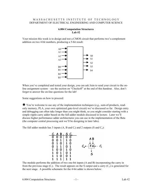
M A S S A C H U S E T T S I N S T I T U T E O F T E C H N O L O G YDEPARTMENT OF ELECTRICAL ENGINEERING AND COMPUTER SCIENCE<strong>6.004</strong> Computation Structures<strong>Lab</strong> <strong>#2</strong>Your mission this week is to design and test a CMOS circuit that performs two’s-complementaddition on two 4-bit numbers, producing a 5-bit result:A0A1A2A3B0B1B2B3S0S1S2S3S4When you’ve completed and tested your design, you can ask Jsim to send your circuit to the onlineassignment system – see the section on “Checkoff” at the end of this handout. Also, don’tforget to answer the on-line questions for the lab!Some suggestions on how to proceed:! You’re welcome to use any of the implementation techniques (e.g., sum-of-products, readonlymemory, PLA, your own optimized gate-level circuit) we’ve discussed so far. Design entryand debugging can often take longer than you might think, so you might consider starting with asimple ripple-carry adder based on the full-adder module discussed in lecture. Later we’lldiscuss higher performance adder architectures you can use in the implementation of the Beta(the computer central processing unit we’ll be designing in later labs).The full adder module has 3 inputs (A, B and C i ) and 2 outputs (S and C o ):The module performs the addition of two one-bit inputs (A and B) incorporating the carry infrom the previous stage (C i ). The result appears on the S output and a carry (C o ) is generated forthe next stage. A possible schematic for the 4-bit adder is shown below:<strong>6.004</strong> Computation Structures - 1 - <strong>Lab</strong> <strong>#2</strong>
A 3 B 3A 2 B 2A 1 B 1A 0 B 0FAFAFAFA“0”S 4S 3S 2S 1S 0! If you have decided to build your design using individual gates, build your own standard celllibrary (e.g., inverter, 2-input NAND, 2-input NOR, 2-input XOR) gates, test them individually,and then use them to assemble your design. It’s much easier to debug your circuit module-bymodulerather than as one big lump. XOR/XNOR can be challenging gates to design; here’s onesuggestion for how they might be implemented:! You can use voltage sources with either a pulse or piece-wise linear waveforms to generatetest signals for your circuit (see <strong>Lab</strong> #1 for details). Another source of test waveforms is the file“/mit/<strong>6.004</strong>/jsim/8clocks.jsim” which can be included in your netlist. It provides eight differentsquare waves (50% duty cycle) with different periods:<strong>6.004</strong> Computation Structures - 2 - <strong>Lab</strong> <strong>#2</strong>
2. Create a MOSFET circuit for each of the logic gates you used in step 1.3. Enter .subckt definitions in your netlist for each of the logic gates. Use Jsim to test eachlogic gate with all possible combinations of inputs. Debugging your gate designs one-byonewill be much easier than trying to debug them as part of the adder circuit. Here’s asample netlist for testing a 2-input NAND gate called nand2:.include "/mit/<strong>6.004</strong>/jsim/nominal.jsim".include "/mit/<strong>6.004</strong>/jsim/8clocks.jsim".subckt nand2 a b z… internals of nand2 circuit here.endsXtest clk1 clk2 z nand2.tran 20ns.plot clk1.plot clk2.plot z4. Enter a .subckt definition for the full-adder, building it out of the gates you designed andtested above. Use Jsim to test your design with all 8 possible combinations of the threeinputs. At this point you probably want to switch to using “Fast Transient Analysis” do tothe simulations as it is much faster than “Device-level Simulation”.5. Enter the netlist for the 4-bit adder and test the circuit using input waveforms supplied bylab2checkoff.jsim. Note that the checkoff circuitry expects your 4-bit adder to haveexactly the terminals shown below – the inside circuitry is up to you, but the “.subcktADDER4…” line in your netlist should match exactly the one shown below..include "/mit/<strong>6.004</strong>/jsim/nominal.jsim".include "/mit/<strong>6.004</strong>/jsim/lab2checkoff.jsim"… subckt definitions of your logic gates.subckt FA a b ci s co… full-adder internals here.ends.subckt ADDER4 a3 a2 a1 a0 b3 b2 b1 b0 s4 s3 s2 s1 s0* remember the node named "0" is the ground node* nodes c0 through c3 are internal to the ADDER moduleXbit0 a0 b0 0 s0 c0 FAXbit1 a1 b1 c0 s1 c1 FAXbit2 a2 b2 c1 s2 c2 FAXbit3 a3 b3 c2 s3 s4 FA.endslab2checkoff.jsim contains the necessary circuitry to generate the appropriate inputwaveforms to test your adder. It includes a .tran statement to run the simulation for theappropriate length of time and a few .plot statements showing the input and outputwaveforms for your circuit.When debugging your circuits, you can plot additional waveforms by adding .plotstatements to the end of your netlist. For example, to plot the carry-out signal from the<strong>6.004</strong> Computation Structures - 4 - <strong>Lab</strong> <strong>#2</strong>
first full adder, you could say.plot Xtest.c0where Xtest is the name lab2checkoff.jsim gave to the ADDER4 device it created and c0is the name of the internal node that connects the carry-out of the low-order FA to thecarry-in of the next FA.Good luck. Don’t be shy about asking questions. ☺CheckoffWhen you are satisfied your circuit works, you can start the checkoff process by making sureyour top-level netlist is visible in the edit window and then clicking on the green checkmark inthe toolbar. Jsim proceeds with the following steps:1. Jsim verifies that a .checkoff statement was found when your netlist was read in.2. Jsim processes each of the .verify statements in turn by retrieving the results of the mostrecent simulation and comparing the computed node values against the supplied expectedvalues. It will report any discrepancies it finds, listing the names of the nodes it waschecking, the simulated time at which it was checking the value, the expected value andthe actual value.3. When the verification process is successful, Jsim asks for your <strong>6.004</strong> user name andpassword (the same ones you use to login to the on-line assignment system) so it cansend the results to the on-line assignment server.4. Jsim sends your circuits to the on-line assignment server, which responds with a statusmessage that will be displayed for you. If you’ve misentered your username or passwordyou can simply click on the green checkmark to try again.As always, if you have any difficulties with checkoff, talk to an LA or TA, or send email to6004−lab@6004.lcs.mit.edu.<strong>6.004</strong> Computation Structures - 5 - <strong>Lab</strong> <strong>#2</strong>

![Semaphores [Printable PDF version]](https://img.yumpu.com/51161588/1/190x245/semaphores-printable-pdf-version.jpg?quality=85)


![Gates and Boolean logic [Printable PDF version] - MIT](https://img.yumpu.com/43807495/1/190x245/gates-and-boolean-logic-printable-pdf-version-mit.jpg?quality=85)