Architecture → Verilog An Extended Example - 6.004
Architecture → Verilog An Extended Example - 6.004
Architecture → Verilog An Extended Example - 6.004
- No tags were found...

You also want an ePaper? Increase the reach of your titles
YUMPU automatically turns print PDFs into web optimized ePapers that Google loves.
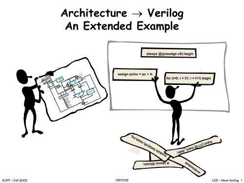
<strong>Architecture</strong> <strong>→</strong> <strong>Verilog</strong><strong>An</strong> <strong>Extended</strong> <strong>Example</strong>always @(posedge clk) beginassign pcinc = pc + 4;for (i=0; i < 31; i = i+1) begin6.371 – Fall 2002 09/11/02L03 – More <strong>Verilog</strong> 1PCSEL 4XAdr OPILLJT32PC+41000A InstructionMemoryDRa: Rb: Rc: +0 1 RA2SELWASELRA1 Register RA2XPRc: 1 WA WA FileWD0RD1 RD2 WE WERFZC:JTPC+4+4*SXT(C)SXT()IRQ ZASEL 1 01 0 BSELControl LogicPCSELRA2SELA BASELALUALUFNWD R/WWrBSELWDSELData MemoryALUFNAdrWrRDWERFWASELPC+40 1 2 WDSELmodule beta(clk,reset,irq,…Input [31:0] mem_data;endmoduleIf (done) $finish;
Reprise: Why use an HDL?• Want an executable functional specification– Document exact behavior of all the modules and their interfaces– Executable models can be tested & refined until they do what you want• Too much detail at the transistor and mask levels– Can’t debug 1M transistors as individual analog components– Abstract away “unnecessary” details– Play by the rules: don’t break abstraction with clever hacks• HDL description is first step in a mostly automated process tobuild an implementation directly from the behavioral model<strong>Verilog</strong>Logic SynthesisGatenetlistPlace & routeMask• HDL<strong>→</strong> logic• map to target library• optimize speed, area• create floorplan blocks• place cells in block• route interconnect• optimize (iterate!)6.371 – Fall 2002 09/11/02L03 – More <strong>Verilog</strong> 2
Beta redux!XAdrILLOPJTI thought I already did<strong>6.004</strong>PCSEL43210PC00AInstructionMemory+4D+PC+4+4*SXT(C)IRQ ZControl LogicXP 1Rc: 0Ra: WASELZC: SXT()WA WAASEL 1 0RA1RD1JTRb: RegisterFile10 1RA2RD20Rc: RA2SELWDWEBSELWERFPCSELRA2SELASELBSELWDSELALUFNWrWERFWASELALUFNAPC+4ALUBData MemoryAdr RDWD R/WWr0 1 2WDSEL6.371 – Fall 2002 09/11/02L03 – More <strong>Verilog</strong> 3
Goals for the <strong>Verilog</strong> description• Readable, correct code that clearly captures the architecture diagram –“correct by inspection”• Partition the design into regions appropriate for different implementationstrategies. Big issue: wires are “bad” since they take up area and havecapacitance (impacting speed and power).– Memories: very dense layouts, structured wires pretty much route themselves,just a few base cells to design & verify– Datapaths: each cell contains necessary wiring, so replicating cells (for N bitsof datapath) also replicates wiring. Data flows between columnar functionalunits on horizontal busses and control flows vertically.– Random logic: interconnect is “random” but library of cells can be designedahead of time and characterized.– Think about physical partition: wires that cross boundaries can take lots ofarea; blocks have to fit into the floorplan without wasteful gaps.Themes: draw as few fets as possible; maximize use of design techniques that offergood wire management strategies; use special tools for each type of layout6.371 – Fall 2002 09/11/02L03 – More <strong>Verilog</strong> 4
Hey! What happened to abstraction?Wasn’t the plan to abstractawaythe physical details sowe could concentrate ongetting the functionalityright? Why are we worryingabout wires and floorplans atthis stage?Because life is short! If you havethe luxury of writing two models(the first to experiment withfunction, the second to describethe actual partition you want tohave), by all means! But with alittle experience you can tackleboth problems at once.6.371 – Fall 2002 09/11/02L03 – More <strong>Verilog</strong> 5
Helping the Tools*In an ideal world it shouldn’t matter how you write the <strong>Verilog</strong> – optimization in theCAD tools will find the best solution. But the world is not ideal (yet…)• Tools work best on smaller problems• Need to partition real problem into pieces for you and the tools (it’s hard tothink about 1M gates at one time). Decompose large problems into smallerproblems and then connect the solutions• Hierarchy in <strong>Verilog</strong> ↔ partitions in physical layout• Tools use your code as a starting point.• Your structure isn’t completed eliminated (this is good…)• Little optimization will be done between top-level blocks• Structure of the problem is often important• Finding a “good” way to think about the problem is keyLike optimizing compilers for C, tools are good for local optimizations but don’texpect them to rewrite your code and change your algorithm. With practice you’lllearn what works and what doesn’t…*adapted from a Stanford EE271 lecture by Mark Horowitz6.371 – Fall 2002 09/11/02L03 – More <strong>Verilog</strong> 6
Divide and conquer…PCSELXAdr4ILLOP3JT2 1PC000A1InstructionMemoryStep 1: identify memoriesStep 2: identify datapathsWhat’s left is random logic…+4DPC2+PC+4+4*SXT(C)IRQ ZXP 1Rc: 0Ra: WASELZC: SXT()RA1WA WARD1JTRb: RegisterFile0 1RA2RD2Rc: RA2SELWDWE1WERFControl LogicASEL 1 010BSELPCSELRA2SELASELBSELWDSELALUFNWrWERFWASELALUFNAPC+4ALUBData MemoryAdr RDWD R/W1WrMain Datapath20 1 2WDSEL6.371 – Fall 2002 09/11/02L03 – More <strong>Verilog</strong> 7
Choosing the right style…• Structural <strong>Verilog</strong>– Use for hierarchy (instantiating other modules)– Floorplanning tools often require that modules which include structuralverilog not include other styles. In other words the leafs of thehierarchy are dataflow/behavioral modules, all other modules are purestructural verilog.• Dataflow <strong>Verilog</strong>: assign target = expression– Use for (most) combinational logic– Avoids problems with activation list omissionsThese two stylesare often mixed in• Behavioral <strong>Verilog</strong>: always @(…) begin … enda single module– Use to model state elements (e.g., registers)– Sometimes useful for combinational logic expressed using for or casestatements– Simulates much faster than dataflow statements since no waveformsare produced for signals internal to behavioral block. Here’s where youcan make the tradeoff between simulation speed and debugability.6.371 – Fall 2002 09/11/02L03 – More <strong>Verilog</strong> 8
Beta Module Hierarchy• beta– control [random logic]– regfile [memory]– pc [datapath]– datapath• dp_misc[datapath]• dp_alu– dp_addsub [datapath]– dp_boole [datapath]– dp_shift [datapath]– dp_cmp [datapath]– dp_mux [datapath]• dp_wdata[datapath]Beta Beta verilog verilogcan can be be found found in in /mit/6.371/examples/beta.vl or or Handouts webpage6.371 – Fall 2002 09/11/02L03 – More <strong>Verilog</strong> 9
Register File// 2-read, 1-write 32-location register filemodule regfile(ra1,rd1,ra2,rd2,clk,werf,wa,wd);input [4:0] ra1; // address for read port 1 (Reg[RA])output [31:0] rd1; // read data for port 1input [4:0] ra2; // address for read port 2 (Reg[RB], Reg[RC] for ST)output [31:0] rd2; // read data for port 2input clk;input werf; // write enable, active highinput [4:0] wa; // address for write port (Reg[RC])input [31:0] wd; // write datareg [31:0] registers[31:0]; // the register file itself (local)// read paths are combinational// logic to ensure R31 reads as zero is in main datapathassign rd1 = registers[ra1];assign rd2 = registers[ra2];// write port is active only when WERF is assertedalways @(posedge clk)if (werf) registers[wa]
= vs.
module pc(clk,reset,pcsel,offset,jump_addr,branch_addr,pc,pc_plus_4);input clk;PCinput reset; // forces PC to 0x80000000input [2:0] pcsel; // selects source of next PCinput [15:0] offset; // inst[15:0]input [31:0] jump_addr; // from Reg[RA], used in JMP instructionoutput [31:0] branch_addr; // send to datapath for LDR instructionoutput [31:0] pc; // used as address for instruction fetchoutput [31:0] pc_plus_4; // saved in regfile during branches, JMP, trapsreg [31:0] pc;wire [30:0] pcinc;wire [31:0] npc;// the Beta PC increments by 4, but won’t change supervisor bitassign pcinc = pc + 4;assign pc_plus_4 = {pc[31],pcinc};// branch address = PC + 4 + 4*sxt(offset)assign branch_addr = {0,pcinc + {{13{offset[15]}},offset[15:0],2'b00}};assign npc = reset ? 32'h80000000 :(pcsel == 0) ? {pc[31],pcinc} : // normal(pcsel == 1) ? {pc[31],branch_addr[30:0]} : // branch(pcsel == 2) ? {pc[31] & jump_addr[31],jump_addr[30:0]} : // jump(pcsel == 3) ? 32'h80000004 : 32'h80000008; // illop, trap// pc register, pc[31] is supervisor bit and gets special treatmentalways @(posedge clk) pc
MainDatapathmodule datapath(inst,rd1,rd2,pc_plus_4,branch_addr,mem_data,rd1zero,rd2zero,asel,bsel,wdsel,alufn,wdata,mem_addr,mem_wdata,z);input [15:0] inst; // constant field from instructioninput [31:0] rd1; // Reg[RA] from register fileinput [31:0] rd2; // Reg[RB] from register file (Reg[RC] for ST)input [31:0] pc_plus_4; // incremented PCinput [31:0] branch_addr; // PC + 4 + 4*sxt(inst[15:0])input [31:0] mem_data; // memory read data (for LD)input rd1zero; // RA == R31, so treat RD1 as 0input rd2zero; // RB/RC == R31, so treat RD2 as 0input asel; // select A operand for ALUinput bsel; // select B operand for ALUinput [1:0] wdsel; // select regfile write datainput [5:0] alufn; // operation to be performed by aluoutput [31:0] wdata; // regfile write data (output of WDSEL mux)output [31:0] mem_addr; // alu output, doubles as data memory addressoutput [31:0] mem_wdata; // data memory write dataoutput z; // true if Reg[RA] is zero, used during brancheswire [31:0] alu_a,alu_b; // A and B inputs to ALU// compute A and B inputs into alu, also Z bit for control logicdp_misc misc(rd1zero,rd2zero,asel,bsel,inst,rd1,rd2,branch_addr,alu_a,alu_b,mem_wdata,z);// where all the heavy-lifting happensdp_alu alu(alufn,alu_a,alu_b,mem_addr);// select regfile write data from PC+4, alu output, and memory datadp_wdata wdata(wdsel,mem_data,mem_addr,pc_plus_4,wdata);endmodule6.371 – Fall 2002 09/11/02L03 – More <strong>Verilog</strong> 13
module dp_addsub(fn,alu_a,alu_b,result,n,v,z);input fn; // 0 for add, 1 for subtractinput [31:0] alu_a; // A operandinput [31:0] alu_b; // B operandoutput [31:0] result; // resultoutput n,v,z; // condition codes computed from resultAdderreg n,v,z;reg [31:0] result;What’sWhat’swrongwrongwith:with:assignassignresultresult==fnfn??aa––bb::aa++b;b;always @(fn or alu_a or alu_b) begin: rippleinteger i; // FOR loop index, not in hardwarereg cin,p,g; // expanded at compile time into many signalsreg [31:0] xb; // hold's complement of ALU_B during subtract// simple ripple-carry adder for nowxb = fn ? ~alu_b : alu_b; // a - b == a + ~b + 1cin = fn; // carry-in is 0 for add, 1 for sub// remember: this FOR is expanded at *compile* timefor (i = 0; i < 32; i = i + 1) beginp = alu_a[i] ^ xb[i]; // carry propagateg = alu_a[i] & xb[i]; // carry generateresult[i] = p ^ cin;cin = g | (p & cin); // carry into next stageendn = result[31]; // negativez = ~|result; // zerov = (alu_a[31] & xb[31] & !n) | (~alu_a[31] & ~xb[31] & n); // overflowendendmodule6.371 – Fall 2002 09/11/02L03 – More <strong>Verilog</strong> 14
…reg [17:0] ctl; // localalways @(inst or interrupt) begin// control romif (interrupt)ctl = 16'b0100100000000000; // interruptelse case (inst[31:26])// ppp aaaaaaww// bcccw lllllldd// tsssaabuuuuuuss// eeeesssffffffeex// sllleeennnnnnllw// t210lll54321010rdefault: ctl = 16'b0011100000000000; // illegal opcode6'b011000: ctl = 16'b0000001000000100; // LD6'b011001: ctl = 16'b0000001000000101; // ST6'b011011: ctl = 16'b0010000000000000; // JMP…6'b111101: ctl = 16'b0000001100001010; // SHRC6'b111110: ctl = 16'b0000001100011010; // SRACendcaseend6.371 – Fall 2002 09/11/02Instructiondecode(fragment)assign werf = ~ctl[0];assign mem_we = !reset & ctl[0];assign wdsel = ctl[2:1];assign alufn = ctl[8:3];assign bsel = ctl[9];assign asel = ctl[10];assign wa = ctl[11] ? 5'b11110 : inst[25:21];assign pcsel = ((ctl[14:12] == 3'b001) & (ctl[15] ^ z)) ? 3'b000 : ctl[14:12];…L03 – More <strong>Verilog</strong> 15
module main;reg clk,reset,irq;wire [31:0] inst_addr,inst_data;wire [31:0] mem_addr,mem_rd_data,mem_wr_data;wire mem_we;Test Jigreg [31:0] memory[1023:0];beta beta(clk,reset,irq,inst_addr,inst_data,mem_addr,mem_rd_data,mem_we,mem_wr_data);// main memory (2 async read ports, 1 sync write port)assign inst_data = memory[inst_addr[13:2]];assign mem_rd_data = memory[mem_addr[13:2]];always @(posedge clk)if (mem_we) memory[mem_addr[13:2]]
![Semaphores [Printable PDF version]](https://img.yumpu.com/51161588/1/190x245/semaphores-printable-pdf-version.jpg?quality=85)


![Gates and Boolean logic [Printable PDF version] - MIT](https://img.yumpu.com/43807495/1/190x245/gates-and-boolean-logic-printable-pdf-version-mit.jpg?quality=85)