Toward non destructive high resolution thermal methods for electric ...
Toward non destructive high resolution thermal methods for electric ...
Toward non destructive high resolution thermal methods for electric ...

You also want an ePaper? Increase the reach of your titles
YUMPU automatically turns print PDFs into web optimized ePapers that Google loves.
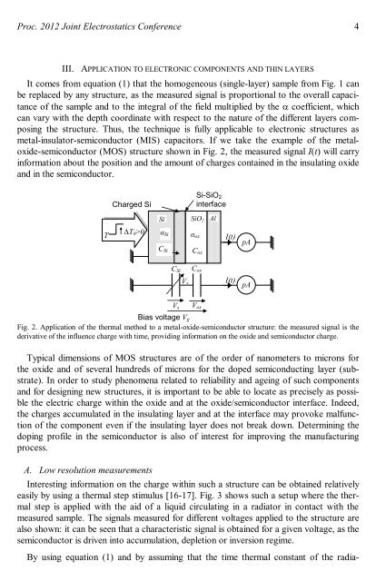
Proc. 2012 Joint Electrostatics Conference 4III. APPLICATION TO ELECTRONIC COMPONENTS AND THIN LAYERSIt comes from equation (1) that the homogeneous (single-layer) sample from Fig. 1 canbe replaced by any structure, as the measured signal is proportional to the overall capacitanceof the sample and to the integral of the field multiplied by the coefficient, whichcan vary with the depth coordinate with respect to the nature of the different layers composingthe structure. Thus, the technique is fully applicable to electronic structures asmetal-insulator-semiconductor (MIS) capacitors. If we take the example of the metaloxide-semiconductor(MOS) structure shown in Fig. 2, the measured signal I(t) will carryin<strong>for</strong>mation about the position and the amount of charges contained in the insulating oxideand in the semiconductor.TCharged SiareaΔT 0 >0Si-SiO 2interfaceSi SiO 2 Alα Si αoxI(t)C SiC oxpAC SiV sC oxI(t)pAV sV oxBias voltage V gFig. 2. Application of the <strong>thermal</strong> method to a metal-oxide-semiconductor structure: the measured signal is thederivative of the influence charge with time, providing in<strong>for</strong>mation on the oxide and semiconductor charge.Typical dimensions of MOS structures are of the order of nanometers to microns <strong>for</strong>the oxide and of several hundreds of microns <strong>for</strong> the doped semiconducting layer (substrate).In order to study phenomena related to reliability and ageing of such componentsand <strong>for</strong> designing new structures, it is important to be able to locate as precisely as possiblethe <strong>electric</strong> charge within the oxide and at the oxide/semiconductor interface. Indeed,the charges accumulated in the insulating layer and at the interface may provoke malfunctionof the component even if the insulating layer does not break down. Determining thedoping profile in the semiconductor is also of interest <strong>for</strong> improving the manufacturingprocess.A. Low <strong>resolution</strong> measurementsInteresting in<strong>for</strong>mation on the charge within such a structure can be obtained relativelyeasily by using a <strong>thermal</strong> step stimulus [16-17]. Fig. 3 shows such a setup where the <strong>thermal</strong>step is applied with the aid of a liquid circulating in a radiator in contact with themeasured sample. The signals measured <strong>for</strong> different voltages applied to the structure arealso shown: it can be seen that a characteristic signal is obtained <strong>for</strong> a given voltage, as thesemiconductor is driven into accumulation, depletion or inversion regime.By using equation (1) and by assuming that the time <strong>thermal</strong> constant of the radia-