Toward non destructive high resolution thermal methods for electric ...
Toward non destructive high resolution thermal methods for electric ...
Toward non destructive high resolution thermal methods for electric ...

You also want an ePaper? Increase the reach of your titles
YUMPU automatically turns print PDFs into web optimized ePapers that Google loves.
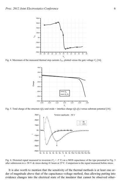
ChargeProc. 2012 Joint Electrostatics Conference 680pA60pA40pA20pAI Max0A-20pA-40pA-60pA-6V -5V -4V -3V -2V -1V 0V 1V 2V 3V 4V 5V 6VFig. 4. Maximum of the measured <strong>thermal</strong> step currents I Max plotted versus the gate voltage V g [16].V g40nC20nC0C -20nC-40nC-60nC-80nCQ 0 Q 0-Q s-100nC-0,6V -0,4V -0,2V 0,0V 0,2V 0,4V 0,6VV sFig. 5. Total charge of the structure (Q 0 ) and oxide + interface charge (Q 0 -Q S ) versus substrate potential [16].Fig. 6. Distorted signal measured in inversion (V g = -5 V) on a MOS capacitance of the type presented in Fig. 3after submission to a -50 V dc stress during 41 hours at 25°C. Comparison to the signal measured be<strong>for</strong>e stress.It is also worth to mention that the sensitivity of the <strong>thermal</strong> <strong>methods</strong> is at least one orderof magnitude above that of the capacitance-voltage method, thus allowing putting intoevidence changes into the <strong>electric</strong>al state of the insulator that cannot be observed other-