Toward non destructive high resolution thermal methods for electric ...
Toward non destructive high resolution thermal methods for electric ...
Toward non destructive high resolution thermal methods for electric ...

You also want an ePaper? Increase the reach of your titles
YUMPU automatically turns print PDFs into web optimized ePapers that Google loves.
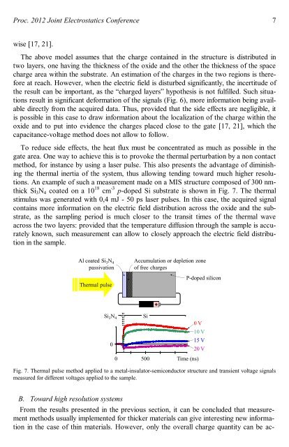
Proc. 2012 Joint Electrostatics Conference 7wise [17, 21].The above model assumes that the charge contained in the structure is distributed intwo layers, one having the thickness of the oxide and the other the thickness of the spacecharge area within the substrate. An estimation of the charges in the two regions is there<strong>for</strong>eat reach. However, when the <strong>electric</strong> field is disturbed significantly, the incertitude ofthe result can be important, as the “charged layers” hypothesis is not fulfilled. Such situationsresult in significant de<strong>for</strong>mation of the signals (Fig. 6), more in<strong>for</strong>mation being availabledirectly from the acquired data. Thus, provided that the side effects are negligible, itis possible in this case to draw in<strong>for</strong>mation about the localization of the charge within theoxide and to put into evidence the charges placed close to the gate [17, 21], which thecapacitance-voltage method does not allow to follow.To reduce side effects, the heat flux must be concentrated as much as possible in thegate area. One way to achieve this is to provoke the <strong>thermal</strong> perturbation by a <strong>non</strong> contactmethod, <strong>for</strong> instance by using a laser pulse. This also presents the advantage of diminishingthe <strong>thermal</strong> inertia of the system, thus allowing tending toward much <strong>high</strong>er <strong>resolution</strong>s.An example of such a measurement made on a MIS structure composed of 300 nmthickSi 3 N 4 coated on a 10 18 cm -3 p-doped Si substrate is shown in Fig. 7. The <strong>thermal</strong>stimulus was generated with 0,4 mJ - 50 ps laser pulses. In this case, the acquired signalcontains more in<strong>for</strong>mation on the <strong>electric</strong> field distribution across the oxide and the substrate,as the sampling period is much closer to the transit times of the <strong>thermal</strong> waveacross the two layers: provided that the temperature diffusion through the sample is accuratelyknown, such measurement can allow to closely approach the <strong>electric</strong> field distributionin the sample.Al coated Si 3 N 4passivationThermal pulseAccumulation or depletion zoneof free chargesP-doped siliconSi 3 N 40Si0 V0 500 Time (ns)Fig. 7. Thermal pulse method applied to a metal-insulator-semiconductor structure and transient voltage signalsmeasured <strong>for</strong> different voltages applied to the sample.10 V15 V20 VB. <strong>Toward</strong> <strong>high</strong> <strong>resolution</strong> systemsFrom the results presented in the previous section, it can be concluded that measurement<strong>methods</strong> usually implemented <strong>for</strong> thicker materials can give interesting new in<strong>for</strong>mationin the case of thin materials. However, only the overall charge quantity can be ac-