Agilent E4438C ESG Vector Signal Generator - Advanced Test ...
Agilent E4438C ESG Vector Signal Generator - Advanced Test ...
Agilent E4438C ESG Vector Signal Generator - Advanced Test ...
Create successful ePaper yourself
Turn your PDF publications into a flip-book with our unique Google optimized e-Paper software.
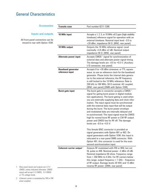
General CharacteristicsAccessoriesInputs and outputsAll front panel connectors can bemoved to rear with Option 1EM.Transits case Part number 9211-129610 MHz input Accepts a 1, 2, 5, or 10 MHz ±0.2 ppm [high-stabilitytimebase] reference signal for operation with anexternal timebase. Nominal input level –3.5 to+20 dBm, impedance 50 Ω. [BNC, rear panel]10 MHz output Outputs the 10 MHz reference signal. Levelnominally +3.9 dBm ±2 dB. Nominal outputimpedance 50 Ω. [BNC, rear panel]Alternate power inputBaseband generatorreference inputAccepts CMOS 1 signal for synchronization ofexternal data and alternate power signal timing.The damage levels are –0.5 to +5.5 V. [AuxiliaryI/O connector, rear panel]Accepts 0 to +20 dBm sinewave, or TTL squarewave,to use as reference clock for the basebandgenerator. Phase locks the internal data generatorto the external reference; the RF frequencyis still locked to the 10 MHz reference. Rate is250 kHz to 100 MHz, 50 Ω nominal, AC coupled.[BNC, rear panel] [SMB with Option 1EM]Burst gate input The burst gate in connector accepts a CMOS 1signal for gating burst power in digital modulationapplications. The burst gating is used whenyou are externally supplying data and clock information.The input signal must be synchronizedwith the external data input that will be outputduring the burst. The burst power envelopeand modulated data are internally delayed andre-synchronized. The input signal must be CMOShigh for normal burst RF power or CW RF outputpower and CMOS low for RF off. The damagelevels are –0.5 to +5.5 V.1. Rear panel inputs and outputs are 3.3 VCMOS, unless indicated otherwise. CMOSinputs will accept 5 V CMOS, 3 V CMOS,or TTL voltage levels.2. Coherent carrier is modulated by FM or FMwhen enabled.Coherent carrier output 228This female BNC connector is provided onsignal generators with Option 601 or 602. Onsignal generators with Option 1EM, this input isrelocated to a rear panel SMB connector. WithOption 401, this connector is used for the evensecond synchronization input.Outputs RF modulated with FM or ΦM, but notIQ, pulse or AM. Nominal power –2 dBm ±5 dB.Nominal impedance 50 ohms. Frequency rangefrom > 250 MHz to 4 GHz. For RF carriers belowthis range, output frequency = 1 GHz – frequencyof RF output. Damage levels 20 VDC and 13 dBmreverse RF power. [SMA, rear panel]


