

AD7745/AD7746 24-Bit Capacitance-to-Digital ... - Analog Devices
AD7745/AD7746 24-Bit Capacitance-to-Digital ... - Analog Devices
AD7745/AD7746 24-Bit Capacitance-to-Digital ... - Analog Devices

You also want an ePaper? Increase the reach of your titles
YUMPU automatically turns print PDFs into web optimized ePapers that Google loves.
FEATURES<br />
<strong>Capacitance</strong>-<strong>to</strong>-digital converter<br />
New standard in single chip solutions<br />
Interfaces <strong>to</strong> single or differential floating sensors<br />
Resolution down <strong>to</strong> 4 aF (that is, up <strong>to</strong> 21 ENOB)<br />
Accuracy: 4 fF<br />
Linearity: 0.01%<br />
Common-mode (not changing) capacitance up <strong>to</strong> 17 pF<br />
Full-scale (changing) capacitance range: ±4 pF<br />
Tolerant of parasitic capacitance <strong>to</strong> ground up <strong>to</strong> 60 pF<br />
Update rate: 10 Hz <strong>to</strong> 90 Hz<br />
Simultaneous 50 Hz and 60 Hz rejection at 16 Hz<br />
Temperature sensor on-chip<br />
Resolution: 0.1°C, accuracy: ±2°C<br />
Voltage input channel<br />
Internal clock oscilla<strong>to</strong>r<br />
2-wire serial interface (I 2 C®-compatible)<br />
Power<br />
2.7 V <strong>to</strong> 5.25 V single-supply operation<br />
0.7 mA current consumption<br />
Operating temperature: –40°C <strong>to</strong> +125°C<br />
16-lead TSSOP package<br />
APPLICATIONS<br />
Au<strong>to</strong>motive, industrial, and medical systems for<br />
Pressure measurement<br />
Position sensing<br />
Level sensing<br />
Flowmeters<br />
Humidity sensing<br />
Impurity detection<br />
VIN(+)<br />
VIN(–)<br />
CIN1(+)<br />
CIN1(–)<br />
EXCA<br />
EXCB<br />
TEMP<br />
SENSOR<br />
CAP DAC<br />
CAP DAC<br />
EXCITATION<br />
MUX<br />
CLOCK<br />
GENERATOR<br />
<strong>24</strong>-BIT Σ-∆<br />
MODULATOR<br />
VDD<br />
DIGITAL<br />
FILTER<br />
VOLTAGE<br />
REFERENCE<br />
REFIN(+) REFIN(–) GND<br />
Figure 1.<br />
Rev. 0<br />
Information furnished by <strong>Analog</strong> <strong>Devices</strong> is believed <strong>to</strong> be accurate and reliable.<br />
However, no responsibility is assumed by <strong>Analog</strong> <strong>Devices</strong> for its use, nor for any<br />
infringements of patents or other rights of third parties that may result from its use.<br />
Specifications subject <strong>to</strong> change without notice. No license is granted by implication<br />
or otherwise under any patent or patent rights of <strong>Analog</strong> <strong>Devices</strong>. Trademarks and<br />
registered trademarks are the property of their respective owners.<br />
<strong>24</strong>-<strong>Bit</strong> <strong>Capacitance</strong>-<strong>to</strong>-<strong>Digital</strong> Converter<br />
with Temperature Sensor<br />
<strong>AD7745</strong>/<strong>AD7746</strong><br />
GENERAL DESCRIPTION<br />
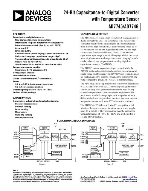
FUNCTIONAL BLOCK DIAGRAMS<br />
<strong>AD7745</strong><br />
I 2 C<br />
SERIAL<br />
INTERFACE<br />
CONTROL LOGIC<br />
CALIBRATION<br />
SDA<br />
SCL<br />
RDY<br />
05468-001<br />
The <strong>AD7745</strong>/<strong>AD7746</strong> are a high resolution, Σ-Δ capacitance-<strong>to</strong>digital<br />
converter (CDC). The capacitance <strong>to</strong> be measured is<br />
connected directly <strong>to</strong> the device inputs. The architecture features<br />
inherent high resolution (<strong>24</strong>-bit no missing codes, up <strong>to</strong><br />
21-bit effective resolution), high linearity (±0.01%), and high<br />
accuracy (±4 fF fac<strong>to</strong>ry calibrated). The <strong>AD7745</strong>/<strong>AD7746</strong><br />
capacitance input range is ±4 pF (changing), while it can accept<br />
up <strong>to</strong> 17 pF common-mode capacitance (not changing), which<br />
can be balanced by a programmable on-chip, digital-<strong>to</strong>capacitance<br />
converter (CAPDAC).<br />
The <strong>AD7745</strong> has one capacitance input channel, while the<br />
<strong>AD7746</strong> has two channels. Each channel can be configured as<br />
single-ended or differential. The <strong>AD7745</strong>/<strong>AD7746</strong> are designed<br />
for floating capacitive sensors. For capacitive sensors with one<br />
plate connected <strong>to</strong> ground, the AD7747 is recommended.<br />
The parts have an on-chip temperature sensor with a resolution<br />
of 0.1°C and accuracy of ±2°C. The on-chip voltage reference<br />
and the on-chip clock genera<strong>to</strong>r eliminate the need for any<br />
external components in capacitive sensor applications. The<br />
parts have a standard voltage input, which <strong>to</strong>gether with the<br />
differential reference input allows easy interface <strong>to</strong> an external<br />
temperature sensor, such as an RTD, thermis<strong>to</strong>r, or diode.<br />
The <strong>AD7745</strong>/<strong>AD7746</strong> have a 2-wire, I 2 C-compatible serial<br />
interface. Both parts can operate with a single power supply<br />
from 2.7 V <strong>to</strong> 5.25 V. They are specified over the au<strong>to</strong>motive<br />
temperature range of –40°C <strong>to</strong> +125°C and are housed in a<br />
16-lead TSSOP package.<br />
VIN(+)<br />
VIN(–)<br />
CIN1(+)<br />
CIN1(–)<br />
CIN2(+)<br />
CIN2(–)<br />
EXC1<br />
EXC2<br />
TEMP<br />
SENSOR<br />
CAP DAC<br />
CAP DAC<br />
EXCITATION<br />
MUX<br />
CLOCK<br />
GENERATOR<br />
<strong>24</strong>-BIT Σ-∆<br />
MODULATOR<br />
VDD<br />
DIGITAL<br />
FILTER<br />
CONTROL LOGIC<br />
CALIBRATION<br />
VOLTAGE<br />
REFERENCE<br />
REFIN(+) REFIN(–) GND<br />
Figure 2.<br />
<strong>AD7746</strong><br />
I 2 C<br />
SERIAL<br />
INTERFACE<br />
One Technology Way, P.O. Box 9106, Norwood, MA 02062-9106, U.S.A.<br />
Tel: 781.329.4700 www.analog.com<br />
Fax: 781.461.3113 © 2005 <strong>Analog</strong> <strong>Devices</strong>, Inc. All rights reserved.<br />
SDA<br />
SCL<br />
RDY<br />
05468-002
<strong>AD7745</strong>/<strong>AD7746</strong><br />
TABLE OF CONTENTS<br />
Specifications..................................................................................... 3<br />
Timing Specifications....................................................................... 5<br />
Absolute Maximum Ratings............................................................ 6<br />
Pin Configurations and Function Descriptions ........................... 7<br />
Typical Performance Characteristics ............................................. 8<br />
Output Noise and Resolution Specifications .............................. 11<br />
Serial Interface ................................................................................ 12<br />
Read Operation........................................................................... 12<br />
Write Operation.......................................................................... 12<br />
<strong>AD7745</strong>/<strong>AD7746</strong> Reset ............................................................. 13<br />
General Call................................................................................. 13<br />
Register Descriptions ..................................................................... 14<br />
Status Register............................................................................. 15<br />
Cap Data Register....................................................................... 15<br />
VT Data Register ........................................................................ 15<br />
Cap Set-Up Register................................................................... 16<br />
VT Set-Up Register .................................................................... 16<br />
EXC Set-Up Register.................................................................. 17<br />
Configuration Register .............................................................. 18<br />
Cap DAC A Register................................................................... 19<br />
Cap DAC B Register................................................................... 19<br />
Cap Offset Calibration Register................................................ 19<br />
REVISION HISTORY<br />
4/05—Revision 0: Initial Version<br />
Rev. 0 | Page 2 of 28<br />
Cap Gain Calibration Register.................................................. 19<br />
Volt Gain Calibration Register ................................................. 19<br />
Circuit Description......................................................................... 20<br />
Overview ..................................................................................... 20<br />
<strong>Capacitance</strong>-<strong>to</strong>-<strong>Digital</strong> Converter ........................................... 20<br />
Excitation Source........................................................................ 20<br />
CAPDAC ..................................................................................... 21<br />
Single-Ended Capacitive Input................................................. 21<br />
Differential Capacitive Input .................................................... 21<br />
Parasitic <strong>Capacitance</strong> <strong>to</strong> Ground.............................................. 22<br />
Parasitic Resistance <strong>to</strong> Ground................................................. 22<br />
Parasitic Parallel Resistance ...................................................... 22<br />
Parasitic Serial Resistance ......................................................... 23<br />
Capacitive Gain Calibration ..................................................... 23<br />
Capacitive System Offset Calibration...................................... 23<br />
Internal Temperature Sensor .................................................... 23<br />
External Temperature Sensor ................................................... <strong>24</strong><br />
Voltage Input ............................................................................... <strong>24</strong><br />
VDD Moni<strong>to</strong>r ................................................................................ <strong>24</strong><br />
Typical Application Diagram.................................................... <strong>24</strong><br />
Outline Dimensions ....................................................................... 25<br />
Ordering Guide .......................................................................... 25
SPECIFICATIONS<br />
VDD = 2.7 V <strong>to</strong> 3.6 V or 4.75 V <strong>to</strong> 5.25 V; GND = 0 V; EXC = 32 kHz; EXC = ±VDD/2; –40°C <strong>to</strong> +125°C, unless otherwise noted.<br />
Rev. 0| Page 3 of 28<br />
<strong>AD7745</strong>/<strong>AD7746</strong><br />
Table 1.<br />
Parameter Min Typ Max Unit Test Conditions/Comments<br />
CAPACITIVE INPUT<br />
Conversion Input Range ±4.096 pF 1 Fac<strong>to</strong>ry calibrated<br />
Integral Nonlinearity (INL) 2 ±0.01 % of FSR<br />
No Missing Codes 2 <strong>24</strong> <strong>Bit</strong> Conversion time ≥ 62 ms<br />
Resolution, p-p 16.5 <strong>Bit</strong> Conversion time = 62 ms, see Table 5<br />
Resolution Effective 19 <strong>Bit</strong> Conversion time = 62 ms, see Table 5<br />
Output Noise, rms 2 aF/√Hz See Table 5<br />
Absolute Error3 ±4 fF1 25°C, VDD = 5 V, after offset calibration<br />
Offset Error2, 4 32 aF1 After system offset calibration,<br />
Excluding effect of noise4 System Offset Calibration Range2 ±1 pF<br />
Offset Drift vs. Temperature –1 aF/°C<br />
Gain Error5 0.02 0.08 % of FS 25°C, VDD = 5 V<br />
Gain Drift vs. Temperature2 –28 –26 –<strong>24</strong> ppm of FS/°C<br />
Allowed <strong>Capacitance</strong> <strong>to</strong> GND2 60 pF See Figure 9 and Figure 10<br />
Power Supply Rejection 0.3 1 fF/V<br />
Normal Mode Rejection 65 dB 50 Hz ± 1%, conversion time = 62 ms<br />
55 dB 60 Hz ± 1%, conversion time = 62 ms<br />
Channel-<strong>to</strong>-Channel Isolation<br />
CAPDAC<br />
70 dB <strong>AD7746</strong> only<br />
Full Range 17 21 pF<br />
Resolution6 164 fF 7-bit CAPDAC<br />
Drift vs. Temperature2 EXCITATION<br />
<strong>24</strong> 26 28 ppm of FS/°C<br />
Frequency 32 kHz<br />
Voltage Across <strong>Capacitance</strong> ±VDD/8 V Configurable via digital interface<br />
±VDD/4 V<br />
±VDD × 3/8 V<br />
±VDD/2 V<br />
Average DC Voltage Across<br />
<strong>Capacitance</strong><br />
<strong>AD7745</strong>/<strong>AD7746</strong><br />
Parameter Min Typ Max Unit Test Conditions/Comments<br />
Full-Scale Drift vs. Temperature 5 ppm of FS/°C Internal reference<br />
0.5 ppm of FS/°C External reference<br />
Average VIN Input Current 300 nA/V<br />
<strong>Analog</strong> VIN Input Current Drift ±50 pA/V/°C<br />
Power Supply Rejection 80 dB Internal reference, VIN = VREF/2<br />
Power Supply Rejection 90 dB External reference, VIN = VREF/2<br />
Normal Mode Rejection 75 dB 50 Hz ± 1%, conversion time = 122.1 ms<br />
50 dB 60 Hz ± 1%, conversion time = 122.1 ms<br />
Common-Mode Rejection 95 dB VIN = 1 V<br />
INTERNAL VOLTAGE REFERENCE<br />
Voltage 1.169 1.17 1.171 V TA = 25°C<br />
Drift vs. Temperature 5 ppm/°C<br />
EXTERNAL VOLTAGE REFERENCE INPUT<br />
Differential REFIN Voltage 2 0.1 2.5 VDD V<br />
Absolute REFIN Voltage 2 GND − 0.03 VDD + 0.03 V<br />
Average REFIN Input Current 400 nA/V<br />
Average REFIN Input Current Drift ±50 pA/V/°C<br />
Common-Mode Rejection 80 dB<br />
SERIAL INTERFACE LOGIC INPUTS<br />
(SCL, SDA)<br />
VIH Input High Voltage 2.1 V<br />
VIL Input Low Voltage 0.8 V<br />
Hysteresis 150 mV<br />
Input Leakage Current (SCL) ±0.1 ±1 µA<br />
OPEN-DRAIN OUTPUT (SDA)<br />
VOL Output Low Voltage 0.4 V ISINK = −6.0 mA<br />
IOH Output High Leakage Current<br />
LOGIC OUTPUT (RDY)<br />
0.1 1 µA VOUT = VDD<br />
VOL Output Low Voltage 0.4 V ISINK = 1.6 mA, VDD = 5 V<br />
VOH Output High Voltage 4.0 V ISOURCE = 200 µA, VDD = 5 V<br />
VOL Output Low Voltage 0.4 V ISINK = 100 µA, VDD = 3 V<br />
VOH Output High Voltage<br />
POWER REQUIREMENTS<br />
VDD – 0.6 V ISOURCE = 100 µA, VDD = 3 V<br />
VDD-<strong>to</strong>-GND Voltage 4.75 5.25 V VDD = 5 V, nominal<br />
2.7 3.6 V VDD = 3.3 V, nominal<br />
IDD Current 850 µA <strong>Digital</strong> inputs equal <strong>to</strong> VDD or GND<br />
750 µA VDD = 5 V<br />
700 µA VDD = 3.3 V<br />
IDD Current Power-Down Mode 0.5 2 µA <strong>Digital</strong> inputs equal <strong>to</strong> VDD or GND<br />
1 <strong>Capacitance</strong> units: 1 pF = 10 -12 F; 1 fF = 10 -15 F; 1 aF = 10 -18 F.<br />
2 Specification is not production tested, but is supported by characterization data at initial product release.<br />
3 Fac<strong>to</strong>ry calibrated. The absolute error includes fac<strong>to</strong>ry gain calibration error, integral nonlinearity error, and offset error after system offset calibration, all at 25°C. At<br />
different temperatures, compensation for gain drift over temperature is required.<br />
4 The capacitive input offset can be eliminated using a system offset calibration. The accuracy of the system offset calibration is limited by the offset calibration register<br />
LSB size (32 aF) or by converter + system p-p noise during the system capacitive offset calibration, whichever is greater. To minimize the effect of the converter +<br />
system noise, longer conversion times should be used for system capacitive offset calibration. The system capacitance offset calibration range is ±1 pF, the larger<br />
offset can be removed using CAPDACs.<br />
5 The gain error is fac<strong>to</strong>ry calibrated at 25°C. At different temperatures, compensation for gain drift over temperature is required.<br />
6 The CAPDAC resolution is seven bits in the actual CAPDAC full range. Using the on-chip offset calibration or adjusting the capacitive offset calibration register can<br />
further reduce the CIN offset or the unchanging CIN component.<br />
7 The VTCHOP bit in the VT SETUP register must be set <strong>to</strong> 1 for the specified temperature sensor and voltage input performance.<br />
8 Using an external temperature sensing diode 2N3906, with nonideality fac<strong>to</strong>r nf = 1.008, connected as in Figure 41, with <strong>to</strong>tal serial resistance
TIMING SPECIFICATIONS<br />
Rev. 0| Page 5 of 28<br />
<strong>AD7745</strong>/<strong>AD7746</strong><br />
VDD = 2.7 V <strong>to</strong> 3.6 V, or 4.75 V <strong>to</strong> 5.25 V; GND = 0 V; Input Logic 0 = 0 V; Input Logic 1 = VDD; –40°C <strong>to</strong> +125°C, unless otherwise noted.<br />
Table 2.<br />
Parameter Min Typ Max Unit Test Conditions/Comments<br />
SERIAL INTERFACE 1, 2 See Figure 3<br />
SCL Frequency 0 400 kHz<br />
SCL High Pulse Width, tHIGH 0.6 µs<br />
SCL Low Pulse Width, tLOW 1.3 µs<br />
SCL, SDA Rise Time, tR 0.3 µs<br />
SCL, SDA Fall Time, tF 0.3 µs<br />
Hold Time (Start Condition), tHD;STA 0.6 µs After this period, the first clock is generated<br />
Set-Up Time (Start Condition), tSU;STA 0.6 µs Relevant for repeated start condition<br />
Data Set-Up Time, tSU;DAT 0.25 µs VDD ≥ 3.0 V<br />
Data Set-Up Time, tSU;DAT 0.35 µs VDD < 3.0 V<br />
Set-Up Time (S<strong>to</strong>p Condition), tSU;STO 0.6 µs<br />
Data Hold Time, tHD;DAT (Master) 0 µs<br />
Bus-Free Time (Between S<strong>to</strong>p and Start Condition, tBUF) 1.3 µs<br />
1 Sample tested during initial release <strong>to</strong> ensure compliance.<br />
2 All input signals are specified with input rise/fall times = 3 ns, measured between the 10% and 90% points. Timing reference points at 50% for inputs and outputs.<br />
Output load = 10 pF.<br />
SCL<br />
SDA<br />
tBUF P S<br />
t LOW<br />
t R<br />
tHIGH tHD:STA tHD:DAT tSU:DAT<br />
tF<br />
Figure 3. Serial Interface Timing Diagram<br />
S<br />
t SU:STA<br />
t HD:STA<br />
t SU:STO<br />
P<br />
05468-003
<strong>AD7745</strong>/<strong>AD7746</strong><br />
ABSOLUTE MAXIMUM RATINGS<br />
TA = 25°C, unless otherwise noted.<br />
Table 3.<br />
Parameter Rating<br />
Positive Supply Voltage VDD <strong>to</strong> GND −0.3 V <strong>to</strong> +6.5 V<br />
Voltage on any Input or Output Pin <strong>to</strong><br />
GND<br />
–0.3 V <strong>to</strong> VDD + 0.3 V<br />
ESD Rating (ESD Association Human Body<br />
Model, S5.1)<br />
2000 V<br />
Operating Temperature Range –40°C <strong>to</strong> +125°C<br />
S<strong>to</strong>rage Temperature Range –65°C <strong>to</strong> +150°C<br />
Junction Temperature 150°C<br />
TSSOP Package θJA,<br />
(Thermal Impedance-<strong>to</strong>-Air)<br />
128°C/W<br />
TSSOP Package θJC,<br />
(Thermal Impedance-<strong>to</strong>-Case)<br />
Lead Temperature, Soldering<br />
14°C/W<br />
Vapor Phase (60 sec) 215°C<br />
Infrared (15 sec) 220°C<br />
ESD CAUTION<br />
Rev. 0 | Page 6 of 28<br />
Stresses above those listed under Absolute Maximum Ratings<br />
may cause permanent damage <strong>to</strong> the device. This is a stress<br />
rating only and functional operation of the device at these or<br />
any other conditions above those indicated in the operational<br />
section of this specification is not implied. Exposure <strong>to</strong> absolute<br />
maximum rating conditions for extended periods may affect<br />
device reliability.<br />
ESD (electrostatic discharge) sensitive device. Electrostatic charges as high as 4000 V readily accumulate on the<br />
human body and test equipment and can discharge without detection. Although this product features<br />
proprietary ESD protection circuitry, permanent damage may occur on devices subjected <strong>to</strong> high energy<br />
electrostatic discharges. Therefore, proper ESD precautions are recommended <strong>to</strong> avoid performance<br />
degradation or loss of functionality.
PIN CONFIGURATIONS AND FUNCTION DESCRIPTIONS<br />
SCL<br />
RDY<br />
EXCA<br />
EXCB<br />
REFIN(+)<br />
REFIN(–)<br />
CIN1(–)<br />
1<br />
2<br />
3<br />
4<br />
5<br />
6<br />
7<br />
<strong>AD7745</strong><br />
TOP VIEW<br />
(Not <strong>to</strong> Scale)<br />
16<br />
15<br />
14<br />
13<br />
12<br />
11<br />
10<br />
SDA<br />
NC<br />
VDD<br />
GND<br />
VIN(–)<br />
VIN(+)<br />
NC<br />
CIN1(+) 8<br />
9 NC<br />
NC = NO CONNECT 05468-004<br />
Figure 4. <strong>AD7745</strong> Pin Configuration (16-Lead TSSOP)<br />
Rev. 0| Page 7 of 28<br />
SCL<br />
RDY<br />
EXCA<br />
EXCB<br />
REFIN(+)<br />
REFIN(–)<br />
CIN1(–)<br />
1<br />
2<br />
3<br />
4<br />
5<br />
6<br />
7<br />
<strong>AD7746</strong><br />
TOP VIEW<br />
(Not <strong>to</strong> Scale)<br />
CIN1(+) 8<br />
9 CIN2(+)<br />
NC = NO CONNECT05468-005 16<br />
15<br />
14<br />
13<br />
12<br />
11<br />
10<br />
<strong>AD7745</strong>/<strong>AD7746</strong><br />
SDA<br />
NC<br />
VDD<br />
GND<br />
VIN(–)<br />
VIN(+)<br />
CIN2(–)<br />
Figure 5. <strong>AD7746</strong> Pin Configuration (16-Lead TSSOP)<br />
Table 4. Pin Function Descriptions<br />
Pin No. Mnemonic Description<br />
1 SCL Serial Interface Clock Input. Connects <strong>to</strong> the master clock line. Requires pull-up resis<strong>to</strong>r if not already<br />
provided in the system.<br />
2 RDY Logic Output. A falling edge on this output indicates that a conversion on enabled channel(s) has been<br />
finished and the new data is available. Alternatively, the status register can be read via the 2-wire serial<br />
interface and the relevant bit(s) decoded <strong>to</strong> query the finished conversion. If not used, this pin should be left<br />
as an open circuit.<br />
3, 4 EXCA, EXCB CDC Excitation Outputs. The measured capacitance is connected between one of the EXC pins and one of the<br />
CIN pins. If not used, these pins should be left as an open circuit.<br />
5, 6 REFIN(+),<br />
REFIN(–)<br />
Differential Voltage Reference Input for the Voltage Channel (ADC). Alternatively, the on-chip internal<br />
reference can be used for the voltage channel. These reference input pins are not used for conversion on<br />
capacitive channel(s) (CDC). If not used, these pins can be left as an open circuit or connected <strong>to</strong> GND.<br />
7 CIN1(–) CDC Negative Capacitive Input in Differential Mode. This pin is internally disconnected in single-ended CDC<br />
configuration. If not used, this pin can be left as an open circuit or connected <strong>to</strong> GND.<br />
8 CIN1(+) CDC Capacitive Input (in Single-Ended Mode) or Positive Capacitive Input (in Differential Mode). The<br />
measured capacitance is connected between one of the EXC pins and one of the CIN pins. If not used, this pin<br />
can be left as an open circuit or connected <strong>to</strong> GND.<br />
9, 10<br />
(<strong>AD7745</strong>)<br />
NC Not Connected. This pin should be left as an open circuit.<br />
9<br />
(<strong>AD7746</strong>)<br />
10<br />
(<strong>AD7746</strong>)<br />
CIN2(+) CDC Second Capacitive Input (in Single-Ended Mode) or Positive Capacitive Input (in Differential Mode). If not<br />
used, this pin can be left open circuit or connected <strong>to</strong> GND.<br />
CIN2(–) CDC Negative Capacitive Input in Differential Mode. This pin is internally disconnected in a single-ended CDC<br />
configuration. If not used, this pin can be left as an open circuit or connected <strong>to</strong> GND.<br />
11, 12 VIN(+), VIN(–) Differential Voltage Input for the Voltage Channel (ADC). These pins are also used <strong>to</strong> connect an external<br />
temperature sensing diode. If not used, these pins can be left as an open circuit or connected <strong>to</strong> GND.<br />
13 GND Ground Pin.<br />
14 VDD Power Supply Voltage. This pin should be decoupled <strong>to</strong> GND, using a low impedance capaci<strong>to</strong>r, for example<br />
in combination with a 10 µF tantalum and a 0.1 µF multilayer ceramic.<br />
15 NC Not Connected. This pin should be left as an open circuit.<br />
16 SDA Serial Interface Bidirectional Data. Connects <strong>to</strong> the master data line. Requires a pull-up resis<strong>to</strong>r if not provided<br />
elsewhere in the system.
<strong>AD7745</strong>/<strong>AD7746</strong><br />
TYPICAL PERFORMANCE CHARACTERISTICS<br />
100<br />
INL (ppm)<br />
GAIN ERROR (ppm)<br />
OFFSET ERROR (aF)<br />
80<br />
60<br />
40<br />
20<br />
2000<br />
1000<br />
0<br />
–5 –4 –3 –2 –1 0 1 2 3 4 5<br />
0<br />
–1000<br />
–2000<br />
INPUT CAPACITANCE (pF)<br />
Figure 6. <strong>Capacitance</strong> Input Integral Nonlinearity,<br />
VDD = 5 V, the Same Configuration as in Figure 31<br />
–3000<br />
–50 –25 0 25 50 75 100 125 150<br />
100<br />
75<br />
50<br />
25<br />
TEMPERATURE (°C)<br />
GAIN TC ≈ –26ppm/°C<br />
Figure 7. <strong>Capacitance</strong> Input Offset Drift vs. Temperature,<br />
VDD = 5 V, CIN and EXC Pins Open Circuit<br />
0<br />
–25<br />
–50<br />
–75<br />
–100<br />
–50 –25 0 25 50 75 100 125 150<br />
TEMPERATURE (°C)<br />
Figure 8. <strong>Capacitance</strong> Input Gain Drift vs. Temperature,<br />
VDD = 5 V, CIN(+) <strong>to</strong> EXC = 4 pF, the Same Configuration as in Figure 30<br />
05468-014<br />
05468-015<br />
05468-016<br />
Rev. 0 | Page 8 of 28<br />
CAPACITANCE ERROR (fF)<br />
18<br />
16<br />
14<br />
12<br />
10<br />
8<br />
6<br />
4<br />
2<br />
0<br />
2.7V 3V 3.3V 5V<br />
–2<br />
0 50 100 150 200 250 300 350 400 450 500<br />
CAPACITANCE CIN PIN TO GND (pF)<br />
Figure 9. <strong>Capacitance</strong> Input Error vs. <strong>Capacitance</strong> between CIN and GND.<br />
CIN(+) <strong>to</strong> EXC = 4 pF, CIN(−) <strong>to</strong> EXC = 0 pF, VDD = 2.7 V, 3 V, 3.3 V, and 5 V,<br />
the Same Configuration as in Figure 33<br />
CAPACITANCE ERROR (fF)<br />
18<br />
16<br />
14<br />
12<br />
10<br />
8<br />
6<br />
4<br />
2<br />
0<br />
2.7V 3V 3.3V<br />
–2<br />
0 50 100 150 200 250 300 350 400 450 500<br />
5V<br />
CAPACITANCE CIN PIN TO GND (pF)<br />
Figure 10. <strong>Capacitance</strong> Input Error vs. <strong>Capacitance</strong> between CIN and GND,<br />
CIN(+) <strong>to</strong> EXC = 21 pF, CIN(−) <strong>to</strong> EXC = 23 pF, VDD = 2.7 V, 3 V, 3.3 V, and 5 V,<br />
the Same Configuration as in Figure 34<br />
CAPACITANCE ERROR (fF)<br />
5<br />
4<br />
3<br />
2<br />
1<br />
0<br />
–1<br />
0 50 100 150 200 250 300 350 400 450 500<br />
CAPACITANCE EXC PIN TO GND (pF)<br />
2.7V 3V<br />
3.3V<br />
Figure 11. <strong>Capacitance</strong> Input Error vs. <strong>Capacitance</strong> between EXC and GND,<br />
CIN(+) <strong>to</strong> EXC = 21 pF, CIN(−) <strong>to</strong> EXC = 23 pF, VDD = 2.7 V, 3 V, 3.3 V, and 5 V,<br />
the Same Configuration as in Figure 34<br />
5V<br />
05468-017<br />
05468-018<br />
05468-019
CAPACITANCE ERROR (fF)<br />
CAPACITANCE ERROR (fF)<br />
CAPACITANCE ERROR (pF)<br />
8<br />
6<br />
4<br />
2<br />
0<br />
–2<br />
–4<br />
–6<br />
–8<br />
–10<br />
2.7V<br />
3V<br />
–12<br />
–250 –200 –150 –100 –50 0 50 100 150 200 250<br />
CIN LEAKAGE TO GND (nA)<br />
Figure 12. <strong>Capacitance</strong> Input Error vs. Leakage Current <strong>to</strong> GND,<br />
CIN(+) <strong>to</strong> EXC = 4 pF, CIN(−) <strong>to</strong> EXC = 0 pF,<br />
VDD = 2.7 V and 3 V<br />
8<br />
6<br />
4<br />
2<br />
0<br />
–2<br />
–4<br />
–6<br />
–8<br />
–10<br />
5V<br />
3.3V<br />
–12<br />
–250 –200 –150 –100 –50 0 50 100 150 200 250<br />
CIN LEAKAGE TO GND (nA)<br />
Figure 13. <strong>Capacitance</strong> Input Error vs. Leakage Current <strong>to</strong> GND,<br />
CIN(+) <strong>to</strong> EXC =4 pF, CIN(−) <strong>to</strong> EXC = 0 pF,<br />
VDD=3.3 V and 5 V<br />
10<br />
1<br />
0.1<br />
0.01<br />
0.001<br />
0.0001<br />
1 10 100 1000 10000 100000<br />
PARALLEL RESISTANCE (MΩ)<br />
Figure 14. <strong>Capacitance</strong> Input Error vs. Resistance in Parallel<br />
with Measured <strong>Capacitance</strong><br />
05468-028<br />
05468-030<br />
05468-029<br />
Rev. 0| Page 9 of 28<br />
CAPACITANCE ERROR (fF)<br />
CAPACITANCE ERROR (fF)<br />
CAPDAC CODE DNL (pF)<br />
0<br />
–2<br />
–4<br />
–6<br />
–8<br />
<strong>AD7745</strong>/<strong>AD7746</strong><br />
–10<br />
0 1 2 3 4 5 6 7<br />
0.2<br />
0<br />
–0.2<br />
–0.4<br />
–0.6<br />
–0.8<br />
SERIAL RESISTANCE (kΩ)<br />
Figure 15. <strong>Capacitance</strong> Input Error vs. Serial Resistance,<br />
CIN(+) <strong>to</strong> EXC = 21 pF, CIN(−) <strong>to</strong> EXC = 23 pF, VDD = 5 V,<br />
the Same Configuration as in Figure 34.<br />
–1.0<br />
2.5 3.0 3.5 4.0 4.5 5.0 5.5<br />
V DD (V)<br />
Figure 16. <strong>Capacitance</strong> Input Power Supply Rejection (PSR),<br />
CIN(+) <strong>to</strong> EXC = 4 pF, the Same Configuration as in Figure 30<br />
0.20<br />
0.15<br />
0.10<br />
0.05<br />
0<br />
–0.05<br />
–0.10<br />
–0.15<br />
–0.20<br />
0 16 32 48 64 80 96 112 128<br />
CAPDAC CODE<br />
Figure 17. CAPDAC Differential Nonlinearity (DNL)<br />
05468-031<br />
05468-032<br />
05468-033
<strong>AD7745</strong>/<strong>AD7746</strong><br />
ERROR (°C)<br />
ERROR (°C)<br />
GAIN (dB)<br />
2.0<br />
1.5<br />
1.0<br />
0.5<br />
0<br />
–0.5<br />
–1.0<br />
–1.5<br />
–2.0<br />
–50 –25 0 25 50 75 100 125 150<br />
TEMPERATURE (°C)<br />
Figure 18. Internal Temperature Sensor Error vs. Temperature<br />
1.0<br />
0.5<br />
0<br />
–0.5<br />
–1.0<br />
–1.5<br />
–2.0<br />
–2.5<br />
–3.0<br />
–50 –25 0 25 50 75 100 125 150<br />
TEMPERATURE (°C)<br />
Figure 19. External Temperature Sensor Error vs. Temperature<br />
0<br />
–20<br />
–40<br />
–60<br />
–80<br />
–100<br />
–120<br />
0 100 200 300 400 500 600 700 800 900 1000<br />
INPUT SIGNAL FREQUENCY (Hz)<br />
Figure 20. <strong>Capacitance</strong> Channel Frequency Response,<br />
Conversion Time = 11 ms<br />
05468-034<br />
05468-035<br />
05468-036<br />
Rev. 0 | Page 10 of 28<br />
GAIN (dB)<br />
GAIN (dB)<br />
GAIN (dB)<br />
0<br />
–20<br />
–40<br />
–60<br />
–80<br />
–100<br />
–120<br />
0 50 100 150 200 250 300 350 400<br />
0<br />
–20<br />
–40<br />
–60<br />
–80<br />
–100<br />
INPUT SIGNAL FREQUENCY (Hz)<br />
Figure 21. <strong>Capacitance</strong> Channel Frequency Response,<br />
Conversion Time = 62 ms<br />
–120<br />
0 50 100 150 200 250 300 350 400<br />
0<br />
–20<br />
–40<br />
–60<br />
–80<br />
–100<br />
INPUT SIGNAL FREQUENCY (Hz)<br />
Figure 22. <strong>Capacitance</strong> Channel Frequency Response,<br />
Conversion Time = 109.6 ms<br />
–120<br />
0 50 100 150 200 250 300 350 400<br />
INPUT SIGNAL FREQUENCY (Hz)<br />
Figure 23. Voltage Channel Frequency Response,<br />
Conversion Time = 122.1 ms<br />
05468-037<br />
05468-038<br />
05468-039
OUTPUT NOISE AND RESOLUTION SPECIFICATIONS<br />
The <strong>AD7745</strong>/<strong>AD7746</strong> resolution is limited by noise. The noise<br />
performance varies with the selected conversion time.<br />
Table 5 shows typical noise performance and resolution for the<br />
capacitive channel. These numbers were generated from 1000<br />
data samples acquired in continuous conversion mode, at an<br />
excitation of 32 kHz, ±VDD/2, and with all CIN and EXC pins<br />
connected only <strong>to</strong> the evaluation board (no external capaci<strong>to</strong>rs.)<br />
Table 5. Typical Capacitive Input Noise and Resolution vs. Conversion Time<br />
Conversion<br />
Time (ms)<br />
Output Data<br />
Rate (Hz)<br />
–3dB Frequency<br />
(Hz)<br />
RMS Noise<br />
(aF/√Hz)<br />
Rev. 0| Page 11 of 28<br />
<strong>AD7745</strong>/<strong>AD7746</strong><br />
Table 6 and Table 7 show typical noise performance and<br />
resolution for the voltage channel. These numbers were<br />
generated from 1000 data samples acquired in continuous<br />
conversion mode with VIN pins shorted <strong>to</strong> ground.<br />
RMS noise represents the standard deviation and p-p noise<br />
represents the difference between minimum and maximum<br />
results in the data. Effective resolution is calculated from rms<br />
noise, and p-p resolution is calculated from p-p noise.<br />
RMS<br />
Noise (aF)<br />
P-P<br />
Noise (aF)<br />
Effective Resolution<br />
(<strong>Bit</strong>s)<br />
11.0 90.9 87.2 4.3 40.0 212.4 17.6 15.2<br />
11.9 83.8 79.0 3.1 27.3 137.7 18.2 15.9<br />
20.0 50.0 43.6 1.8 12.2 82.5 19.4 16.6<br />
38.0 26.3 21.8 1.6 7.3 50.3 20.1 17.3<br />
62.0 16.1 13.8 1.5 5.4 33.7 20.5 17.9<br />
77.0 13.0 10.5 1.5 4.9 28.3 20.7 18.1<br />
92.0 10.9 8.9 1.5 4.4 27.8 20.8 18.2<br />
109.6 9.1 8.0 1.5 4.2 27.3 20.9 18.2<br />
Table 6. Typical Voltage Input Noise and Resolution vs. Conversion Time, Internal Voltage Reference<br />
Conversion<br />
Time (ms)<br />
Output Data<br />
Rate (Hz)<br />
–3dB Frequency<br />
(Hz)<br />
RMS Noise<br />
(µV)<br />
P-P Noise<br />
(µV)<br />
Effective Resolution<br />
(<strong>Bit</strong>s)<br />
20.1 49.8 26.4 11.4 62 17.6 15.2<br />
32.1 31.2 15.9 7.1 42 18.3 15.7<br />
62.1 16.1 8.0 4.0 28 19.1 16.3<br />
122.1 8.2 4.0 3.0 20 19.5 16.8<br />
Table 7. Typical Voltage Input Noise and Resolution vs. Conversion Time, External 2.5 V Voltage Reference<br />
Conversion<br />
Time (ms)<br />
Output Data<br />
Rate (Hz)<br />
–3dB Frequency<br />
(Hz)<br />
RMS Noise<br />
(µV)<br />
P-P Noise<br />
(µV)<br />
Effective Resolution<br />
(<strong>Bit</strong>s)<br />
20.1 49.8 26.4 14.9 95 18.3 15.6<br />
32.1 31.2 15.9 6.3 42 19.6 16.8<br />
62.1 16.1 8.0 3.3 22 20.5 17.7<br />
122.1 8.2 4.0 2.1 15 21.1 18.3<br />
P-P Resolution<br />
(<strong>Bit</strong>s)<br />
P-P Resolution<br />
(<strong>Bit</strong>s)<br />
P-P Resolution<br />
(<strong>Bit</strong>s)
<strong>AD7745</strong>/<strong>AD7746</strong><br />
SERIAL INTERFACE<br />
The <strong>AD7745</strong>/<strong>AD7746</strong> supports an I2C-compatible 2-wire serial<br />
interface. The two wires on the I2C bus are called SCL (clock)<br />
and SDA (data). These two wires carry all addressing, control,<br />
and data information one bit at a time over the bus <strong>to</strong> all<br />
connected peripheral devices. The SDA wire carries the data,<br />
while the SCL wire synchronizes the sender and receiver during<br />
the data transfer. I2C devices are classified as either master or<br />
slave devices. A device that initiates a data transfer message is<br />
called a master, while a device that responds <strong>to</strong> this message is<br />
called a slave.<br />
To control the <strong>AD7745</strong>/<strong>AD7746</strong> device on the bus, the<br />
following pro<strong>to</strong>col must be followed. First, the master initiates a<br />
data transfer by establishing a start condition, defined by a<br />
high-<strong>to</strong>-low transition on SDA while SCL remains high. This<br />
indicates that the start byte follows. This 8-bit start byte is made<br />
up of a 7-bit address plus an R/W bit indica<strong>to</strong>r.<br />
All peripherals connected <strong>to</strong> the bus respond <strong>to</strong> the start<br />
condition and shift in the next 8 bits (7-bit address + R/W bit).<br />
The bits arrive MSB first. The peripheral that recognizes the<br />
transmitted address responds by pulling the data line low<br />
during the ninth clock pulse. This is known as the acknowledge<br />
bit. All other devices withdraw from the bus at this point and<br />
maintain an idle condition. An exception <strong>to</strong> this is the general<br />
call address, which is described later in this document. The idle<br />
condition is where the device moni<strong>to</strong>rs the SDA and SCL lines<br />
waiting for the start condition and the correct address byte. The<br />
R/W bit determines the direction of the data transfer. A Logic 0<br />
LSB in the start byte means that the master writes information<br />
<strong>to</strong> the addressed peripheral. In this case the <strong>AD7745</strong>/<strong>AD7746</strong><br />
becomes a slave receiver. A Logic 1 LSB in the start byte means<br />
that the master reads information from the addressed peripheral.<br />
In this case, the <strong>AD7745</strong>/<strong>AD7746</strong> becomes a slave<br />
transmitter. In all instances, the <strong>AD7745</strong>/<strong>AD7746</strong> acts as a<br />
standard slave device on the I2C bus.<br />
The start byte address for the <strong>AD7745</strong>/<strong>AD7746</strong> is 0x90 for a<br />
write and 0x91 for a read.<br />
READ OPERATION<br />
When a read is selected in the start byte, the register that is<br />
currently addressed by the address pointer is transmitted on <strong>to</strong><br />
the SDA line by the <strong>AD7745</strong>/<strong>AD7746</strong>. This is then clocked out<br />
by the master device and the <strong>AD7745</strong>/<strong>AD7746</strong> awaits an<br />
acknowledge from the master.<br />
If an acknowledge is received from the master, the address au<strong>to</strong>incrementer<br />
au<strong>to</strong>matically increments the address pointer<br />
register and outputs the next addressed register content on <strong>to</strong><br />
the SDA line for transmission <strong>to</strong> the master. If no acknowledge<br />
is received, the <strong>AD7745</strong>/<strong>AD7746</strong> return <strong>to</strong> the idle state and the<br />
address pointer is not incremented.<br />
Rev. 0 | Page 12 of 28<br />
The address pointers’ au<strong>to</strong>-incrementer allow block data <strong>to</strong> be<br />
written or read from the starting address and subsequent<br />
incremental addresses.<br />
In continuous conversion mode, the address pointers’ au<strong>to</strong>incrementer<br />
should be used for reading a conversion result.<br />
That means, the three data bytes should be read using one<br />
multibyte read transaction rather than three separate single byte<br />
transactions. The single byte data read transaction may result in<br />
the data bytes from two different results being mixed. The same<br />
applies for six data bytes if both the capacitive and the<br />
voltage/temperature channel are enabled.<br />
The user can also access any unique register (address) on a one<strong>to</strong>-one<br />
basis without having <strong>to</strong> update all the registers. The<br />
address pointer register contents cannot be read.<br />
If an incorrect address pointer location is accessed or, if the user<br />
allows the au<strong>to</strong>-incrementer <strong>to</strong> exceed the required register<br />
address, the following applies:<br />
• In read mode, the <strong>AD7745</strong>/<strong>AD7746</strong> continues <strong>to</strong> output<br />
various internal register contents until the master device<br />
issues a no acknowledge, start, or s<strong>to</strong>p condition. The<br />
address pointers’ au<strong>to</strong>-incrementer’s contents are reset <strong>to</strong><br />
point <strong>to</strong> the status register at Address 0x00 when a s<strong>to</strong>p<br />
condition is received at the end of a read operation. This<br />
allows the status register <strong>to</strong> be read (polled) continually<br />
without having <strong>to</strong> constantly write <strong>to</strong> the address pointer.<br />
• In write mode, the data for the invalid address is not loaded<br />
in<strong>to</strong> the <strong>AD7745</strong>/<strong>AD7746</strong> registers but an acknowledge is<br />
issued by the <strong>AD7745</strong>/<strong>AD7746</strong>.<br />
WRITE OPERATION<br />
When a write is selected, the byte following the start byte is<br />
always the register address pointer (subaddress) byte, which<br />
points <strong>to</strong> one of the internal registers on the <strong>AD7745</strong>/ <strong>AD7746</strong>.<br />
The address pointer byte is au<strong>to</strong>matically loaded in<strong>to</strong> the<br />
address pointer register and acknowledged by the <strong>AD7745</strong>/<br />
<strong>AD7746</strong>. After the address pointer byte acknowledge, a s<strong>to</strong>p<br />
condition, a repeated start condition, or another data byte can<br />
follow from the master.<br />
A s<strong>to</strong>p condition is defined by a low-<strong>to</strong>-high transition on SDA<br />
while SCL remains high. If a s<strong>to</strong>p condition is ever encountered<br />
by the <strong>AD7745</strong>/<strong>AD7746</strong>, it returns <strong>to</strong> its idle condition and the<br />
address pointer is reset <strong>to</strong> Address 0x00.<br />
If a data byte is transmitted after the register address pointer<br />
byte, the <strong>AD7745</strong>/<strong>AD7746</strong> load this byte in<strong>to</strong> the register that is<br />
currently addressed by the address pointer register, send an<br />
acknowledge, and the address pointer au<strong>to</strong>-incrementer au<strong>to</strong>matically<br />
increments the address pointer register <strong>to</strong> the next<br />
internal register address. Thus, subsequent transmitted data<br />
bytes are loaded in<strong>to</strong> sequentially incremented addresses.
If a repeated start condition is encountered after the address<br />
pointer byte, all peripherals connected <strong>to</strong> the bus respond<br />
exactly as outlined above for a start condition, that is, a repeated<br />
start condition is treated the same as a start condition. When a<br />
master device issues a s<strong>to</strong>p condition, it relinquishes control of<br />
the bus, allowing another master device <strong>to</strong> take control of the<br />
bus. Hence, a master wanting <strong>to</strong> retain control of the bus issues<br />
successive start conditions known as repeated start conditions.<br />
<strong>AD7745</strong>/<strong>AD7746</strong> RESET<br />
To reset the <strong>AD7745</strong>/<strong>AD7746</strong> without having <strong>to</strong> reset the entire<br />
I 2 C bus, an explicit reset command is provided. This uses a<br />
particular address pointer word as a command word <strong>to</strong> reset the<br />
part and upload all default settings. The <strong>AD7745</strong>/<strong>AD7746</strong> do<br />
not respond <strong>to</strong> the I 2 C bus commands (do not acknowledge)<br />
during the default values upload for approximately 150 µs<br />
(max 200 µs).<br />
The reset command address word is 0xBF.<br />
WRITE<br />
SEQUENCE<br />
READ<br />
SEQUENCE<br />
SDATA<br />
SCLOCK<br />
S SLAVE ADDR A(S) SUB ADDR A(S)<br />
LSB = 0<br />
S<br />
Rev. 0| Page 13 of 28<br />
GENERAL CALL<br />
<strong>AD7745</strong>/<strong>AD7746</strong><br />
When a master issues a slave address consisting of seven 0s with<br />
the eighth bit (R/W bit) set <strong>to</strong> 0, this is known as the general call<br />
address. The general call address is for addressing every device<br />
connected <strong>to</strong> the I 2 C bus. The <strong>AD7745</strong>/<strong>AD7746</strong> acknowledge<br />
this address and read in the following data byte.<br />
If the second byte is 0x06, the <strong>AD7745</strong>/<strong>AD7746</strong> are reset,<br />
completely uploading all default values. The <strong>AD7745</strong>/<strong>AD7746</strong><br />
do not respond <strong>to</strong> the I 2 C bus commands (do not acknowledge)<br />
during the default values upload for approximately 150 µs (max<br />
200 µs).<br />
The <strong>AD7745</strong>/<strong>AD7746</strong> do not acknowledge any other general<br />
call commands.<br />
1–7 8 9 1–7 8 9 1–7 8 9 P<br />
START ADDR R/W ACK SUBADDRESS ACK DATA ACK STOP<br />
Figure <strong>24</strong>. Bus Data Transfer<br />
DATA A(S)<br />
LSB = 1<br />
05468-006<br />
DATA A(S) P<br />
S SLAVE ADDR A(S) SUB ADDR A(S) S SLAVE ADDR A(S) DATA A(M) DATA A(M) P<br />
S = START BIT<br />
P = STOP BIT<br />
A(S) = ACKNOWLEDGE BY SLAVE<br />
A(M) = ACKNOWLEDGE BY MASTER<br />
Figure 25. Write and Read Sequences<br />
A(S) = NO-ACKNOWLEDGE BY SLAVE<br />
A(M) = NO-ACKNOWLEDGE BY MASTER<br />
05468-007
<strong>AD7745</strong>/<strong>AD7746</strong><br />
REGISTER DESCRIPTIONS<br />
The master can write <strong>to</strong> or read from all of the <strong>AD7745</strong>/<br />
<strong>AD7746</strong> registers except the address pointer register, which is a<br />
write-only register. The address pointer register determines<br />
which register the next read or write operation accesses. All<br />
communications with the part through the bus start with an<br />
access <strong>to</strong> the address pointer register. After the part has been<br />
Rev. 0 | Page 14 of 28<br />
accessed over the bus and a read/write operation is selected, the<br />
address pointer register is set up. The address pointer register<br />
determines from or <strong>to</strong> which register the operation takes place.<br />
A read/write operation is performed from/<strong>to</strong> the target address,<br />
which then increments <strong>to</strong> the next address until a s<strong>to</strong>p<br />
command on the bus is performed.<br />
Table 8. Register Summary<br />
Address<br />
Pointer<br />
<strong>Bit</strong> 7 <strong>Bit</strong> 6 <strong>Bit</strong> 5 <strong>Bit</strong> 4 <strong>Bit</strong> 3 <strong>Bit</strong> 2 <strong>Bit</strong> 1 <strong>Bit</strong> 0<br />
Register (Dec) (Hex) Dir Default Value<br />
Status 0 0x00 R<br />
-<br />
0<br />
-<br />
0<br />
-<br />
0<br />
-<br />
0<br />
EXCERR<br />
0<br />
RDY<br />
1<br />
RDYVT<br />
1<br />
RDYCAP<br />
1<br />
Cap Data H 1 0x01 R Capacitive channel data—high byte, 0x00<br />
Cap Data M 2 0x02 R Capacitive channel data—middle byte, 0x00<br />
Cap Data L 3 0x03 R Capacitive channel data—low byte, 0x00<br />
VT Data H 4 0x04 R Voltage/temperature channel data—high byte, 0x00<br />
VT Data M 5 0x05 R Voltage/temperature channel data—middle byte, 0x00<br />
VT Data L 6 0x06 R Voltage/temperature channel data—low byte, 0x00<br />
Cap Setup 7 0x07 R/W<br />
VT Setup 8 0x08 R/W<br />
EXC Setup 9 0x09 R/W<br />
Configuration 10 0x0A R/W<br />
Cap DAC A 11 0x0B R/W<br />
Cap DAC B 12 0x0C R/W<br />
CAPEN CIN21 CAPDIFF - - - - CAPCHOP<br />
0 0 0 0 0 0 0 0<br />
VTEN VTMD1 VTMD0 EXTREF - - VTSHORT VTCHOP<br />
0 0 0 0 0 0 0 0<br />
CLKCTRL EXCON EXCB EXCB EXCA EXCA EXCLVL1 EXCLVL0<br />
0 0 0 0 0 0 1 1<br />
VTFS1 VTFS0 CAPFS2 CAPFS1 CAPFS0 MD2 MD1 MD0<br />
1 0 1 0 0 0 0 0<br />
DACAENA DACA—7-<strong>Bit</strong> Value<br />
0 0x00<br />
DACBENB DACB—7-<strong>Bit</strong> Value<br />
0 0x00<br />
Cap Offset H 13 0x0D R/W Capacitive offset calibration—high byte, 0x80<br />
Cap Offset L 14 0x0E R/W Capacitive offset calibration—low byte, 0x00<br />
Cap Gain H 15 0x0F R/W Capacitive gain calibration—high byte, fac<strong>to</strong>ry calibrated<br />
Cap Gain L 16 0x10 R/W Capacitive gain calibration—low byte, fac<strong>to</strong>ry calibrated<br />
Volt Gain H 17 0x11 R/W Voltage gain calibration—high byte, fac<strong>to</strong>ry calibrated<br />
Volt Gain L 18 0x12 R/W Voltage gain calibration—low byte, fac<strong>to</strong>ry calibrated<br />
1 The CIN2 bit is relevant only for <strong>AD7746</strong>. The CIN2 bit should always be 0 on the <strong>AD7745</strong>.
STATUS REGISTER<br />
Address Pointer 0x00, Read Only, Default Value 0x07<br />
This register indicates the status of the converter. The status<br />
register can be read via the 2-wire serial interface <strong>to</strong> query a<br />
finished conversion.<br />
Table 9. Status Register <strong>Bit</strong> Map<br />
Rev. 0| Page 15 of 28<br />
<strong>AD7745</strong>/<strong>AD7746</strong><br />
The RDY pin reflects the status of the RDY bit. Therefore, the<br />
RDY pin high-<strong>to</strong>-low transition can be used as an alternative<br />
indication of the finished conversion.<br />
<strong>Bit</strong> <strong>Bit</strong> 7 <strong>Bit</strong> 6 <strong>Bit</strong> 5 <strong>Bit</strong> 4 <strong>Bit</strong> 3 <strong>Bit</strong> 2 <strong>Bit</strong> 1 <strong>Bit</strong> 0<br />
Mnemonic - - - - EXCERR RDY RDYVT RDYCAP<br />
Default 0 0 0 0 0 1 1 1<br />
Table 10.<br />
<strong>Bit</strong> Mnemonic Description<br />
7-4 - Not used, always read 0.<br />
3 EXCERR EXCERR = 1 indicates that the excitation output cannot be driven properly.<br />
The possible reason can be a short circuit or <strong>to</strong>o high capacitance between the excitation pin and ground.<br />
2 RDY RDY = 0 indicates that conversion on the enabled channel(s) has been finished and new unread data is<br />
available.<br />
If both capacitive and voltage/temperature channels are enabled, the RDY bit is changed <strong>to</strong> 0 after conversion<br />
on both channels is finished. The RDY bit returns <strong>to</strong> 1 either when data is read or prior <strong>to</strong> finishing the next<br />
conversion.<br />
If, for example, only the capacitive channel is enabled, then the RDY bit reflects the RDYCAP bit.<br />
1 RDYVT RDYVT = 0 indicates that a conversion on the voltage/temperature channel has been finished and new unread<br />
data is available.<br />
0 RDYCAP RDYCAP = 0 indicates that a conversion on the capacitive channel has been finished and new unread data is<br />
available.<br />
CAP DATA REGISTER<br />
<strong>24</strong> <strong>Bit</strong>s, Address Pointer 0x01, 0x02, 0x03, Read-Only,<br />
Default Value 0x000000<br />
Capacitive channel output data. The register is updated after<br />
finished conversion on the capacitive channel, with one<br />
exception: When the serial interface read operation from the<br />
CAP DATA register is in progress, the data register is not<br />
updated and the new capacitance conversion result is lost.<br />
The s<strong>to</strong>p condition on the serial interface is considered <strong>to</strong> be the<br />
end of the read operation. Therefore, <strong>to</strong> prevent data corruption,<br />
all three bytes of the data register should be read sequentially<br />
using the register address pointer au<strong>to</strong>-increment feature of the<br />
serial interface.<br />
To prevent losing some of the results, the CAP DATA register<br />
should be read before the next conversion on the capacitive<br />
channel is finished.<br />
The 0x000000 code represents negative full scale (–4.096 pF),<br />
the 0x800000 code represents zero scale (0 pF), and the<br />
0xFFFFFF code represents positive full scale (+4.096 pF).<br />
VT DATA REGISTER<br />
<strong>24</strong> <strong>Bit</strong>s, Address Pointer 0x04, 0x05, 0x06, Read-Only,<br />
Default Value 0x000000<br />
Voltage/temperature channel output data. The register is<br />
updated after finished conversion on the voltage channel or<br />
temperature channel, with one exception: When the serial<br />
interface read operation from the VT DATA register is in<br />
progress, the data register is not updated and the new<br />
voltage/temperature conversion result is lost.<br />
The s<strong>to</strong>p condition on the serial interface is considered <strong>to</strong> be the<br />
end of the read operation. Therefore, <strong>to</strong> prevent data corruption,<br />
all three bytes of the data register should be read sequentially<br />
using the register address pointer au<strong>to</strong>-increment feature of the<br />
serial interface.<br />
For voltage input, Code 0 represents negative full scale (–VREF),<br />
the 0x800000 code represents zero scale (0 V), and the<br />
0xFFFFFF code represents positive full scale (+VREF).<br />
To prevent losing some of the results, the VT DATA register<br />
should be read before the next conversion on the voltage/<br />
temperature channel is finished.<br />
For the temperature sensor, the temperature can be calculated<br />
from code using the following equation:<br />
Temperature (°C) = (Code/2048) − 4096
<strong>AD7745</strong>/<strong>AD7746</strong><br />
CAP SET-UP REGISTER<br />
Address Pointer 0x07, Default Value 0x00<br />
Capacitive channel setup.<br />
Table 11. CAP Set-Up Register <strong>Bit</strong> Map<br />
<strong>Bit</strong> <strong>Bit</strong> 7 <strong>Bit</strong> 6 <strong>Bit</strong> 5 <strong>Bit</strong> 4 <strong>Bit</strong> 3 <strong>Bit</strong> 2 <strong>Bit</strong> 1 <strong>Bit</strong> 0<br />
Mnemonic CAPEN CIN2 CAPDIFF - - - - CAPCHOP<br />
Default 0 0 0 0 0 0 0 0<br />
Table 12.<br />
<strong>Bit</strong> Mnemonic Description<br />
7 CAPEN CAPEN = 1 enables capacitive channel for single conversion, continuous conversion, or calibration.<br />
6 CIN2 CIN2 = 1 switches the internal multiplexer <strong>to</strong> the second capacitive input on the <strong>AD7746</strong>.<br />
5 CAPDIFF DIFF = 1 sets differential mode on the selected capacitive input.<br />
4-1 - These bits must be 0 for proper operation.<br />
0 CAPCHOP The CAPCHOP bit should be set <strong>to</strong> 0 for the specified capacitive channel performance.<br />
CAPCHOP = 1 approximately doubles the capacitive channel conversion times and slightly improves the<br />
capacitive channel noise performance for the longest conversion times.<br />
VT SET-UP REGISTER<br />
Address Pointer 0x08, Default Value 0x00<br />
Voltage/Temperature channel setup.<br />
Table 13. VT Set-Up Register <strong>Bit</strong> Map<br />
<strong>Bit</strong> <strong>Bit</strong> 7 <strong>Bit</strong> 6 <strong>Bit</strong> 5 <strong>Bit</strong> 4 <strong>Bit</strong> 3 <strong>Bit</strong> 2 <strong>Bit</strong> 1 <strong>Bit</strong> 0<br />
Mnemonic VTEN VTMD1 VTMD0 EXTREF - - VTSHORT VTCHOP<br />
Default 0 0 0 0 0 0 0 0<br />
Table 14.<br />
<strong>Bit</strong> Mnemonic Description<br />
7 VTEN VTEN = 1 enables voltage/temperature channel for single conversion, continuous conversion, or calibration.<br />
6<br />
5<br />
VTMD1<br />
VTMD0<br />
Voltage/temperature channel input configuration.<br />
VTMD1 VTMD0 Channel Input<br />
0 0 Internal temperature sensor<br />
0 1 External temperature sensor diode<br />
1 0 VDD moni<strong>to</strong>r<br />
1 1 External voltage input (VIN)<br />
4 EXTREF EXTREF = 1 selects an external reference voltage connected <strong>to</strong> REFIN(+), REFIN(–) for the voltage input or the<br />
VDD moni<strong>to</strong>r.<br />
EXTREF = 0 selects the on-chip internal reference. The internal reference must be used with the internal<br />
temperature sensor for proper operation.<br />
3-2 - These bits must be 0 for proper operation.<br />
1 VTSHORT VTSHORT = 1 internally shorts the voltage/temperature channel input for test purposes.<br />
0 VTCHOP = 1 VTCHOP = 1 sets internal chopping on the voltage/temperature channel.<br />
The VTCHOP bit must be set <strong>to</strong> 1 for the specified voltage/temperature channel performance.<br />
Rev. 0 | Page 16 of 28
EXC SET-UP REGISTER<br />
Address Pointer 0x09, Default Value 0x03<br />
Capacitive channel excitation setup.<br />
Table 15. EXC Set-Up <strong>Bit</strong> Map<br />
Rev. 0| Page 17 of 28<br />
<strong>AD7745</strong>/<strong>AD7746</strong><br />
<strong>Bit</strong> <strong>Bit</strong> 7 <strong>Bit</strong> 6 <strong>Bit</strong> 5 <strong>Bit</strong> 4 <strong>Bit</strong> 3 <strong>Bit</strong> 2 <strong>Bit</strong> 1 <strong>Bit</strong> 0<br />
Mnemonic CLKCTRL EXCON EXCB EXCB EXCA EXCA EXCLVL1 EXCLVL0<br />
Default 0 0 0 0 0 0 0 0<br />
Table 16.<br />
<strong>Bit</strong> Mnemonic Description<br />
7 CLKCTRL The CLKCTRL bit should be set <strong>to</strong> 0 for the specified <strong>AD7745</strong>/<strong>AD7746</strong> performance.<br />
CLKCTRL = 1 decreases the excitation signal frequency and the modula<strong>to</strong>r clock frequency by fac<strong>to</strong>r of 2.<br />
This also increases the conversion time on all channels (capacitive, voltage, and temperature) by a fac<strong>to</strong>r of 2.<br />
6 EXCON When EXCON = 0, the excitation signal is present on the output only during capacitance channel conversion.<br />
When EXCON = 1, the excitation signal is present on the output during both capacitance and<br />
voltage/temperature conversion.<br />
5 EXCB EXCB = 1 enables EXCB pin as the excitation output.<br />
4 EXCB EXCB = 1 enables EXCB pin as the inverted excitation output.<br />
Only one of the EXCB or the EXCB bits should be set for proper operation.<br />
3 EXCA EXCA = 1 enables EXCA pin as the excitation output.<br />
2 EXCA EXCA = 1 enables EXCA pin as the inverted excitation output.<br />
Only one of the EXCA or the EXCA bits should be set for proper operation.<br />
1<br />
0<br />
EXCLVL1,<br />
EXCLVL0<br />
Excitation Voltage Level.<br />
EXCLVL1 EXCLVL0 Voltage on Cap EXC Pin Low Level EXC Pin High Level<br />
0 0 ±VDD/8 VDD × 3/8 VDD × 5/8<br />
0 1 ±VDD/4 VDD × 1/4 VDD × 3/4<br />
1 0 ±VDD × 3/8 VDD × 1/8 VDD × 7/8<br />
1 1 ±VDD/2 0 VDD
<strong>AD7745</strong>/<strong>AD7746</strong><br />
CONFIGURATION REGISTER<br />
Address Pointer 0x0A, Default Value 0xA0<br />
Converter update rate and mode of operation setup.<br />
Table 17. Configuration Register <strong>Bit</strong> Map<br />
<strong>Bit</strong> <strong>Bit</strong> 7 <strong>Bit</strong> 6 <strong>Bit</strong> 5 <strong>Bit</strong> 4 <strong>Bit</strong> 3 <strong>Bit</strong> 2 <strong>Bit</strong> 1 <strong>Bit</strong> 0<br />
Mnemonic VTF1 VTF0 CAPF2 CAPF1 CAPF0 MD2 MD1 MD0<br />
Default 0 0 0 0 0 0 0 0<br />
Table 18.<br />
<strong>Bit</strong> Mnemonic Description<br />
7<br />
6<br />
5<br />
4<br />
3<br />
2<br />
1<br />
0<br />
VTF1<br />
VTF0<br />
CAPF2<br />
CAPF1<br />
CAPF0<br />
MD2<br />
MD1<br />
MD0<br />
Voltage/temperature channel digital filter setup—conversion time/update rate setup.<br />
The conversion times in this table are valid for the CLKCTRL = 0 in the EXC SETUP register. The conversion<br />
times are longer by a fac<strong>to</strong>r of two for the CLKCTRL = 1.<br />
VTCHOP = 1<br />
VTF1 VTF0 Conversion Time (ms) Update Rate (Hz) –3 dB Frequency (Hz)<br />
0 0 20.1 49.8 26.4<br />
0 1 32.1 31.2 15.9<br />
1 0 62.1 16.1 8.0<br />
1 1 122.1 8.2 4.0<br />
Capacitive channel digital filter setup—conversion time/update rate setup.<br />
The conversion times in this table are valid for the CLKCTRL = 0 in the EXC SETUP register.<br />
The conversion times are longer by fac<strong>to</strong>r of two for the CLKCTRL = 1.<br />
CAP CHOP = 0<br />
CAPF2 CAPF1 CAPF0 Conversion Time (ms) Update Rate –3 dB Frequency (Hz)<br />
0 0 0 11.0 90.9 87.2<br />
0 0 1 11.9 83.8 79.0<br />
0 1 0 20.0 50.0 43.6<br />
0 1 1 38.0 26.3 21.8<br />
1 0 0 62.0 16.1 13.1<br />
1 0 1 77.0 13.0 10.5<br />
1 1 0 92.0 10.9 8.9<br />
1 1 1 109.6 9.1 8.0<br />
Converter mode of operation setup.<br />
MD2 MD1 MD0 Mode<br />
0 0 0 Idle<br />
0 0 1 Continuous conversion<br />
0 1 0 Single conversion<br />
0 1 1 Power-Down<br />
1 0 0 -<br />
1 0 1 <strong>Capacitance</strong> system offset calibration<br />
1 1 0 <strong>Capacitance</strong> or voltage system gain calibration<br />
1 1 1<br />
Rev. 0 | Page 18 of 28
CAP DAC A REGISTER<br />
Address Pointer 0x0B, Default Value 0x00<br />
Capacitive DAC setup.<br />
Table 19. Cap DAC A Register <strong>Bit</strong> Map<br />
Rev. 0| Page 19 of 28<br />
<strong>AD7745</strong>/<strong>AD7746</strong><br />
<strong>Bit</strong> <strong>Bit</strong> 7 <strong>Bit</strong> 6 <strong>Bit</strong> 5 <strong>Bit</strong> 4 <strong>Bit</strong> 3 <strong>Bit</strong> 2 <strong>Bit</strong> 1 <strong>Bit</strong> 0<br />
Mnemonic DACAENA DACA—7-<strong>Bit</strong> Value<br />
Default 0 0x00<br />
Table 20.<br />
<strong>Bit</strong> Mnemonic Description<br />
7 DACAENA DACAENA = 1 connects capacitive DACA <strong>to</strong> the positive capacitance input.<br />
6-1 DACA DACA value, Code 0x00 ≈ 0 pF, Code 0x7F ≈ full range.<br />
CAP DAC B REGISTER<br />
Address Pointer 0x0C, Default Value 0x00<br />
Capacitive DAC setup.<br />
Table 21. Cap DAC B Register <strong>Bit</strong> Map<br />
<strong>Bit</strong> <strong>Bit</strong> 7 <strong>Bit</strong> 6 <strong>Bit</strong> 5 <strong>Bit</strong> 4 <strong>Bit</strong> 3 <strong>Bit</strong> 2 <strong>Bit</strong> 1 <strong>Bit</strong> 0<br />
Mnemonic DACBENB DACB—7-bit value<br />
Default 0 0x00<br />
Table 22.<br />
<strong>Bit</strong> Mnemonic Description<br />
7 DACBENB DACBENB = 1 connects capacitive DACB <strong>to</strong> the negative capacitance input.<br />
6-1 DACB DACB value, Code 0x00 ≈ 0 pF, Code 0x7F ≈ full range.<br />
CAP OFFSET CALIBRATION REGISTER<br />
16 <strong>Bit</strong>s, Address Pointer 0x0D, 0x0E,<br />
Default Value 0x8000<br />
The capacitive offset calibration register holds the capacitive<br />
channel zero-scale calibration coefficient. The coefficient is<br />
used <strong>to</strong> digitally remove the capacitive channel offset. The<br />
register value is updated au<strong>to</strong>matically following the execution<br />
of a capacitance offset calibration. The capacitive offset calibration<br />
resolution (cap offset register LSB) is less than 32 aF; the<br />
full range is 1 pF.<br />
On the <strong>AD7746</strong>, the register is shared by the two capacitive<br />
channels. If the capacitive channels need <strong>to</strong> be offset-calibrated<br />
individually, the host controller software should read the<br />
<strong>AD7746</strong> capacitive offset calibration register values after<br />
performing the offset calibration on individual channels and<br />
then reload the values back <strong>to</strong> the <strong>AD7746</strong> before executing<br />
conversion on a different channel.<br />
CAP GAIN CALIBRATION REGISTER<br />
16 <strong>Bit</strong>s, Address Pointer 0x0F, 0x10,<br />
Default Value 0xXXXX<br />
Capacitive gain calibration register. The register holds the<br />
capacitive channel full-scale fac<strong>to</strong>ry calibration coefficient.<br />
On the <strong>AD7746</strong>, the register is shared by the two capacitive<br />
channels.<br />
VOLT GAIN CALIBRATION REGISTER<br />
16 <strong>Bit</strong>s, Address Pointer 0x11,0x12,<br />
Default Value 0xXXXX<br />
Voltage gain calibration register. The register holds the voltage<br />
channel full-scale fac<strong>to</strong>ry calibration coefficient.
<strong>AD7745</strong>/<strong>AD7746</strong><br />
CIRCUIT DESCRIPTION<br />
VIN(+)<br />
VIN(–)<br />
CIN1(+)<br />
CIN1(–)<br />
EXCA<br />
EXCB<br />
TEMP<br />
SENSOR<br />
OVERVIEW<br />
CAP DAC<br />
CAP DAC<br />
EXCITATION<br />
MUX<br />
CLOCK<br />
GENERATOR<br />
<strong>24</strong>-BIT Σ-∆<br />
MODULATOR<br />
VDD<br />
DIGITAL<br />
FILTER<br />
CONTROL LOGIC<br />
CALIBRATION<br />
VOLTAGE<br />
REFERENCE<br />
REFIN(+) REFIN(–) GND<br />
Figure 26. <strong>AD7745</strong> Block Diagram<br />
<strong>AD7745</strong><br />
I 2 C<br />
SERIAL<br />
INTERFACE<br />
The <strong>AD7745</strong>/<strong>AD7746</strong> core is a high precision converter consisting<br />
of a second order (Σ-Δ or charge balancing) modula<strong>to</strong>r<br />
and a third order digital filter. It works as a CDC for the capacitive<br />
inputs and as a classic ADC for the voltage input or for<br />
the voltage from a temperature sensor.<br />
In addition <strong>to</strong> the converter, the <strong>AD7745</strong>/<strong>AD7746</strong> integrates a<br />
multiplexer, an excitation source and CAPDACs for the capacitive<br />
inputs, a temperature sensor, a voltage reference for the<br />
voltage and temperature inputs, a complete clock genera<strong>to</strong>r, a<br />
control and calibration logic, and an I 2 C-compatible serial<br />
interface.<br />
The <strong>AD7745</strong> has one capacitive input, while the <strong>AD7746</strong> has<br />
two capacitive inputs. All other features and specifications are<br />
identical for both parts.<br />
CAPACITANCE-TO-DIGITAL CONVERTER<br />
Figure 28 shows the CDC simplified functional diagram. The<br />
measured capacitance CX is connected between the excitation<br />
source and the Σ-Δ modula<strong>to</strong>r input. A square-wave excitation<br />
signal is applied on the CX during the conversion and the<br />
modula<strong>to</strong>r continuously samples the charge going through the<br />
CX. The digital filter processes the modula<strong>to</strong>r output, which is a<br />
stream of 0s and 1s containing the information in 0 and 1<br />
density. The data from the digital filter is scaled, applying the<br />
calibration coefficients, and the final result can be read through<br />
the serial interface.<br />
The <strong>AD7745</strong>/<strong>AD7746</strong> is designed for floating capacitive<br />
sensors. Therefore, both CX plates have <strong>to</strong> be isolated from<br />
ground.<br />
SDA<br />
SCL<br />
RDY<br />
05468-001<br />
VIN(+)<br />
VIN(–)<br />
CIN1(+)<br />
CIN1(–)<br />
CIN2(+)<br />
CIN2(–)<br />
EXC1<br />
EXC2<br />
Rev. 0 | Page 20 of 28<br />
C X<br />
TEMP<br />
SENSOR<br />
CAP DAC<br />
CAP DAC<br />
EXCITATION<br />
CIN<br />
EXC<br />
MUX<br />
EXCITATION SOURCE<br />
CLOCK<br />
GENERATOR<br />
<strong>24</strong>-BIT Σ-∆<br />
MODULATOR<br />
VDD<br />
DIGITAL<br />
FILTER<br />
CONTROL LOGIC<br />
CALIBRATION<br />
VOLTAGE<br />
REFERENCE<br />
REFIN(+) REFIN(–) GND<br />
Figure 27. <strong>AD7746</strong> Block Diagram<br />
CLOCK<br />
GENERATOR<br />
<strong>24</strong>-BIT Σ-∆<br />
MODULATOR<br />
DIGITAL<br />
FILTER<br />
<strong>AD7746</strong><br />
I 2 C<br />
SERIAL<br />
INTERFACE<br />
CAPACITANCE TO DIGITAL CONVERTER<br />
(CDC)<br />
EXCITATION<br />
DATA<br />
Figure 28. CDC Simplified Block Diagram<br />
The two excitation pins EXCA and EXCB are independently<br />
programmable. They are identically functional and therefore<br />
either of them can be used for the capacitive sensor excitation.<br />
On the 2-channel <strong>AD7746</strong> using a separate excitation pin for<br />
each capacitive channel is recommended.<br />
05468-027<br />
SDA<br />
SCL<br />
RDY<br />
05468-002
CAPDAC<br />
The <strong>AD7745</strong>/<strong>AD7746</strong> CDC full-scale input range is ±4.096 pF.<br />
For simplicity of calculation, however, the following text and<br />
diagrams use ±4 pF. The part can accept a higher capacitance<br />
on the input and the common-mode or offset (not-changing<br />
component) capacitance can be balanced by programmable<br />
on-chip CAPDACs.<br />
C X<br />
CIN(+)<br />
CIN(–)<br />
C Y<br />
EXC<br />
CAPDAC(+)<br />
CAPDAC(–)<br />
CDC<br />
Figure 29. Using a CAPDAC<br />
DATA<br />
The CAPDAC can be unders<strong>to</strong>od as a negative capacitance<br />
connected internally <strong>to</strong> the CIN pin. There are two independent<br />
CAPDACs, one connected <strong>to</strong> the CIN(+) and the second<br />
connected <strong>to</strong> the CIN(–). The relation between the capacitance<br />
input and output data can be expressed as<br />
( C − CAPDAC(<br />
+ ) ) − ( C − ( −)<br />
)<br />
DATA X<br />
Y<br />
≈ CAPDAC<br />
The CAPDACs have a 7-bit resolution, mono<strong>to</strong>nic transfer<br />
function, are well matched <strong>to</strong> each other, and have a defined<br />
temperature coefficient. The CAPDAC full range (absolute<br />
value) is not fac<strong>to</strong>ry calibrated and can vary up <strong>to</strong> ±20% with<br />
the manufacturing process. See the Specifications section and<br />
typical performance characteristics in Figure 17.<br />
The CAPDACs are shared by the two capacitive channels on the<br />
<strong>AD7746</strong>. If the CAPDACs need <strong>to</strong> be set individually, the host<br />
controller software should reload the CAPDAC values <strong>to</strong> the<br />
<strong>AD7746</strong> before executing conversion on a different channel.<br />
SINGLE-ENDED CAPACITIVE INPUT<br />
When configured for a single-ended mode (the CAPDIFF bit in<br />
the Cap Setup register is set <strong>to</strong> 0), the <strong>AD7745</strong>/<strong>AD7746</strong> CIN(–)<br />
pin is disconnected internally. The CDC (without using the<br />
CAPDACs) can measure only positive input capacitance in the<br />
range of 0 pF <strong>to</strong> 4 pF (see Figure 30).<br />
C X<br />
0 ... 4pF<br />
CIN(+)<br />
CIN(–)<br />
EXC<br />
CAPDAC(+)<br />
OFF<br />
CAPDIFF = 0<br />
CAPDAC(–)<br />
OFF<br />
0 ... 4pF<br />
CDC<br />
Figure 30. CDC Single-Ended Input Mode<br />
0x800000 ... 0xFFFFFF<br />
DATA<br />
05468-010<br />
05468-0<strong>24</strong><br />
Rev. 0| Page 21 of 28<br />
<strong>AD7745</strong>/<strong>AD7746</strong><br />
The CAPDAC can be used for programmable shifting the input<br />
range. The example in Figure 31 shows how <strong>to</strong> use the full<br />
±4 pF CDC span <strong>to</strong> measure capacitance between 0 pF <strong>to</strong> 8 pF.<br />
C X<br />
0 ... 8pF<br />
CIN(+)<br />
CIN(–)<br />
EXC<br />
CAPDAC(+)<br />
4pF<br />
CAPDIFF = 0<br />
CAPDAC(–)<br />
0pF<br />
± 4pF<br />
CDC<br />
Figure 31. Using CAPDAC in Single-Ended Mode<br />
0x000000 ... 0xFFFFFF<br />
DATA<br />
Figure 32 shows how <strong>to</strong> shift the input range further, up <strong>to</strong><br />
21 pF absolute value of capacitance connected <strong>to</strong> the CIN(+).<br />
C X<br />
13 ... 21pF<br />
(17 ± 4pF)<br />
CIN(+)<br />
CIN(–)<br />
EXC<br />
CAPDAC(+)<br />
17pF<br />
CAPDIFF = 0<br />
CAPDAC(–)<br />
0pF<br />
± 4pF<br />
CDC<br />
Figure 32. Using CAPDAC in Single-Ended Mode<br />
DIFFERENTIAL CAPACITIVE INPUT<br />
0x000000 ... 0xFFFFFF<br />
DATA<br />
When configured for a differential mode (the CAPDIFF bit in<br />
the Cap Setup register set <strong>to</strong> 1), the <strong>AD7745</strong>/<strong>AD7746</strong> CDC<br />
measures the difference between positive and negative<br />
capacitance input.<br />
Each of the two input capacitances CX and CY between the EXC<br />
and CIN pins must be less than 4 pF (without using the<br />
CAPDACs) or must be less than 21 pF and balanced by the<br />
CAPDACs. Balancing by the CAPDACs means that both<br />
CX–CAPDAC(+) and CY–CAPDAC(–) are less than 4 pF.<br />
If the unbalanced capacitance between the EXC and CIN pins is<br />
higher than 4 pF, the CDC introduces a gain error, an offset<br />
error, and nonlinearity error.<br />
See the examples shown in Figure 33, Figure 34, and Figure 35.<br />
C X<br />
0 ... 4pF<br />
CIN(+)<br />
CIN(–)<br />
C Y<br />
0 ... 4pF<br />
EXC<br />
CAPDAC(+)<br />
OFF<br />
CAPDIFF = 1<br />
CAPDAC(–)<br />
OFF<br />
± 4pF<br />
CDC<br />
Figure 33. CDC Differential Input Mode<br />
0x000000 ... 0xFFFFFF<br />
DATA<br />
05468-025<br />
05468-026<br />
05468-020
<strong>AD7745</strong>/<strong>AD7746</strong><br />
C X<br />
15 ... 19pF<br />
(17 ± 2pF)<br />
C X<br />
13 ... 21pF<br />
(17 ± 4pF)<br />
CIN(+)<br />
CIN(–)<br />
C Y<br />
15 ... 19pF<br />
(17 ± 2pF)<br />
EXC<br />
CAPDAC(+)<br />
17pF<br />
CAPDIFF = 1<br />
CAPDAC(–)<br />
17pF<br />
± 4pF<br />
CDC<br />
Figure 34. Using CAPDAC in Differential Mode<br />
CIN(+)<br />
CIN(–)<br />
C Y<br />
17pF<br />
EXC<br />
CAPDAC(+)<br />
17pF<br />
CAPDIFF = 1<br />
CAPDAC(–)<br />
17pF<br />
± 4pF<br />
CDC<br />
Figure 35. Using CAPDAC in Differential Mode<br />
PARASITIC CAPACITANCE TO GROUND<br />
C GND1<br />
C GND2<br />
C X<br />
CIN<br />
EXC<br />
CDC<br />
Figure 36. Parasitic <strong>Capacitance</strong> <strong>to</strong> Ground<br />
0x000000 ... 0xFFFFFF<br />
DATA<br />
0x000000 ... 0xFFFFFF<br />
DATA<br />
DATA<br />
The CDC architecture used in the <strong>AD7745</strong>/<strong>AD7746</strong> measures<br />
the capacitance CX connected between the EXC pin and the<br />
CIN pin. In theory, any capacitance CP <strong>to</strong> ground should not<br />
affect the CDC result (see Figure 36).<br />
The practical implementation of the circuitry in the chip<br />
implies certain limits and the result is gradually affected by<br />
capacitance <strong>to</strong> ground. See the allowed capacitance <strong>to</strong> GND in<br />
the specification table for CIN and excitation. Also see the<br />
typical performance characteristics shown in Figure 9, Figure<br />
10, and Figure 11.<br />
05468-012<br />
05468-021<br />
05468-011<br />
Rev. 0 | Page 22 of 28<br />
PARASITIC RESISTANCE TO GROUND<br />
R GND1 CIN<br />
R GND2<br />
C X<br />
EXC<br />
CDC<br />
Figure 37. Parasitic Resistance <strong>to</strong> Ground<br />
DATA<br />
The <strong>AD7745</strong>/<strong>AD7746</strong> CDC result would be affected by a leakage<br />
current from the CX <strong>to</strong> ground, therefore the CX should be<br />
isolated from the ground. The influence of the leakage current<br />
varies with the power supply voltage. The following limits can<br />
be used as a guideline for the allowed leakage current or the<br />
equivalent resistance between the CX and ground (Figure 37).<br />
VDD ≈ 5 V: IGND < 150 nA (that is, RGND > 30 MΩ)<br />
VDD ≥ 3 V: IGND < 60 nA (that is, RGND > 50 MΩ)<br />
VDD ≥ 2.7 V: IGND < 30 nA (that is, RGND > 100 MΩ)<br />
A higher leakage current <strong>to</strong> ground results in a gain error, an<br />
offset error, and a nonlinearity error. See the typical<br />
performance characteristics shown in Figure 12 and Figure 13.<br />
PARASITIC PARALLEL RESISTANCE<br />
C X<br />
R P<br />
CIN<br />
EXC<br />
CDC<br />
Figure 38. Parasitic Parallel Resistance<br />
DATA<br />
The <strong>AD7745</strong>/<strong>AD7746</strong> CDC measures the charge transfer<br />
between EXC pin and CIN pin. Any resistance connected in<br />
parallel <strong>to</strong> the measured capacitance CX (see Figure 38), such as<br />
the parasitic resistance of the sensor, also transfers charge.<br />
Therefore, the parallel resis<strong>to</strong>r is seen as an additional<br />
capacitance in the output data. The equivalent parallel<br />
capacitance (or error caused by the parallel resistance) can be<br />
approximately calculated as<br />
C<br />
P<br />
1<br />
=<br />
R × F<br />
P<br />
EXC<br />
× 4<br />
Where RP is the parallel resistance and CEXC is the excitation<br />
frequency. See the typical performance characteristics shown in<br />
Figure 14.<br />
05468-022<br />
05468-013
PARASITIC SERIAL RESISTANCE<br />
C X<br />
R S1 CIN<br />
R S2<br />
EXC<br />
CDC<br />
Figure 39. Parasitic Serial Resistance<br />
DATA<br />
The <strong>AD7745</strong>/<strong>AD7746</strong> CDC result is affected by a resistance in<br />
series with the measured capacitance. The <strong>to</strong>tal serial resistance,<br />
which refers <strong>to</strong> RS1 + RS2 on Figure 39, should be less than 1 kΩ<br />
for the specified performance. See typical performance characteristics<br />
shown in Figure 15.<br />
CAPACITIVE GAIN CALIBRATION<br />
The <strong>AD7745</strong>/<strong>AD7746</strong> gain is fac<strong>to</strong>ry calibrated for the full scale<br />
of ±4.096 pF in the production for each part individually. The<br />
fac<strong>to</strong>ry gain coefficient is s<strong>to</strong>red in a one-time programmable<br />
(OTP) memory and is copied <strong>to</strong> the capacitive gain register at<br />
power-up or after reset.<br />
The gain can be changed by executing a capacitance gain<br />
calibration mode, for which an external full-scale capacitance<br />
needs <strong>to</strong> be connected <strong>to</strong> the capacitance input, or by writing a<br />
user value <strong>to</strong> the capacitive gain register. This change would be<br />
only temporary and the fac<strong>to</strong>ry gain coefficient would be<br />
reloaded back after power-up or reset. The part is tested and<br />
specified only for use with the default fac<strong>to</strong>ry calibration<br />
coefficient.<br />
CAPACITIVE SYSTEM OFFSET CALIBRATION<br />
The capacitive offset is dominated by the parasitic offset in the<br />
application, such as the initial capacitance of the sensor, any<br />
parasitic capacitance of tracks on the board, and the capacitance<br />
of any other connections between the sensor and the CDC.<br />
Therefore, the <strong>AD7745</strong>/<strong>AD7746</strong> are not fac<strong>to</strong>ry calibrated for<br />
capacitive offset. It is the user’s responsibility <strong>to</strong> calibrate the<br />
system capacitance offset in the application.<br />
Any offset in the capacitance input larger than ±1 pF should<br />
first be removed using the on-chip CAPDACs. The small offset<br />
within ±1 pF can then be removed by using the capacitance<br />
offset calibration register.<br />
One method of adjusting the offset is <strong>to</strong> connect a zero-scale<br />
capacitance <strong>to</strong> the input and execute the capacitance offset<br />
calibration mode. The calibration sets the midpoint of the<br />
±4.096 pF range (that is, Output Code 0x800000) <strong>to</strong> that<br />
zero-scale input.<br />
Another method would be <strong>to</strong> calculate and write the offset calibration<br />
register value, the LSB is value 31.25 aF (4.096 pF/2 17 ).<br />
05468-023<br />
Rev. 0| Page 23 of 28<br />
<strong>AD7745</strong>/<strong>AD7746</strong><br />
The offset calibration register is reloaded by the default value at<br />
power-on or after reset. Therefore, if the offset calibration is not<br />
repeated after each system power-up, the calibration coefficient<br />
value should be s<strong>to</strong>red by the host controller and reloaded as<br />
part of the <strong>AD7745</strong>/<strong>AD7746</strong> setup.<br />
On the <strong>AD7746</strong>, the register is shared by the two capacitive<br />
channels. If the capacitive channels need <strong>to</strong> be offset calibrated<br />
individually, the host controller software should read the<br />
<strong>AD7746</strong> capacitive offset calibration register values after<br />
performing the offset calibration on individual channels and<br />
then reload the values back <strong>to</strong> the <strong>AD7746</strong> before executing a<br />
conversion on a different channel.<br />
INTERNAL TEMPERATURE SENSOR<br />
INTERNAL TEMPERATURE SENSOR<br />
I N × I<br />
∆V BE<br />
CLOCK<br />
GENERATOR<br />
<strong>24</strong>-BIT Σ-∆<br />
MODULATOR<br />
VOLTAGE<br />
REFERENCE<br />
V DD<br />
DIGITAL<br />
FILTER<br />
AND<br />
SCALING<br />
DATA<br />
Figure 40. Internal Temperature Sensor<br />
The temperature sensing method used in the <strong>AD7745</strong>/<strong>AD7746</strong><br />
is <strong>to</strong> measure a difference in ∆VBE voltage of a transis<strong>to</strong>r<br />
operated at two different currents (see Figure 40). The ∆VBE<br />
change with temperature is linear and can be expressed as<br />
∆<br />
where:<br />
KT<br />
= ( n ) × ln( N)<br />
q<br />
VBE f<br />
K is Boltzmann’s constant (1.38 × 10 –23 ).<br />
T is the absolute temperature in Kelvin.<br />
q is the charge on the electron (1.6 × 10 –19 coulombs).<br />
N is the ratio of the two currents.<br />
nf is the ideality fac<strong>to</strong>r of the thermal diode.<br />
The <strong>AD7745</strong>/<strong>AD7746</strong> uses an on-chip transis<strong>to</strong>r <strong>to</strong> measure the<br />
temperature of the silicon chip inside the package. The Σ-Δ<br />
ADC converts the ∆VBE <strong>to</strong> digital, the data are scaled using<br />
fac<strong>to</strong>ry calibration coefficients, thus the output code is<br />
proportional <strong>to</strong> temperature:<br />
( ) 4096<br />
2048 − = °<br />
Code<br />
Temperatur e C<br />
The <strong>AD7745</strong>/<strong>AD7746</strong> has a low power consumption resulting<br />
in only a small effect due <strong>to</strong> the part self-heating (less than<br />
0.5°C at VDD = 5 V).<br />
05468-040
<strong>AD7745</strong>/<strong>AD7746</strong><br />
If the capacitive sensor can be considered <strong>to</strong> be at the same<br />
temperature as the <strong>AD7745</strong>/<strong>AD7746</strong> chip, the internal<br />
temperature sensor can be used as a system temperature sensor.<br />
That means the complete system temperature drift<br />
compensation can be based on the <strong>AD7745</strong>/<strong>AD7746</strong> internal<br />
temperature sensor without need for any additional external<br />
components. See the typical performance characteristics in<br />
Figure 18.<br />
EXTERNAL TEMPERATURE SENSOR<br />
EXTERNAL<br />
TEMPERATURE<br />
SENSOR<br />
2N3906<br />
∆V BE<br />
RS1 VIN (+)<br />
RS2 VIN (–)<br />
I ... N × I<br />
V DD<br />
CLOCK<br />
GENERATOR<br />
<strong>24</strong>-BIT Σ-∆<br />
MODULATOR<br />
VOLTAGE<br />
REFERENCE<br />
DIGITAL<br />
FILTER<br />
AND<br />
SCALING<br />
DATA<br />
Figure 41. Transis<strong>to</strong>r as an External Temperature Sensor<br />
The <strong>AD7745</strong>/<strong>AD7746</strong> provide the option of using an external<br />
transis<strong>to</strong>r as a temperature sensor in the system. The ∆VBE<br />
method, which is similar <strong>to</strong> the internal temperature sensor<br />
method, is used. However, it is modified <strong>to</strong> compensate for the<br />
serial resistance of connections <strong>to</strong> the sensor. Total serial<br />
resistance (RS1 + RS2 in Figure 41) up <strong>to</strong> 100 Ω is compensated.<br />
The VIN(–) pin must be grounded for proper external<br />
temperature sensor operation.<br />
The <strong>AD7745</strong>/<strong>AD7746</strong> are fac<strong>to</strong>ry calibrated for<br />
Transis<strong>to</strong>r 2N3906 with the ideality fac<strong>to</strong>r nf = 1.008.<br />
See the typical performance characteristics shown<br />
in Figure 19.<br />
TYPICAL APPLICATION DIAGRAM<br />
VIN(+)<br />
VIN(–)<br />
CIN1(+)<br />
CIN1(–)<br />
EXCA<br />
EXCB<br />
TEMP<br />
SENSOR<br />
CAP DAC<br />
CAP DAC<br />
EXCITATION<br />
MUX<br />
05468-041<br />
CLOCK<br />
GENERATOR<br />
<strong>24</strong>-BIT Σ-∆<br />
MODULATOR<br />
REFIN(+) REFIN(–)<br />
VDD<br />
DIGITAL<br />
FILTER<br />
Rev. 0 | Page <strong>24</strong> of 28<br />
VOLTAGE INPUT<br />
R T<br />
R REF<br />
VOLTAGE<br />
REFERENCE<br />
RTD<br />
VIN(+)<br />
VIN(–)<br />
REFIN(+)<br />
REFIN(–)<br />
VDD<br />
ANALOG TO DIGITAL CONVERTER<br />
(ADC)<br />
CLOCK<br />
GENERATOR<br />
<strong>24</strong>-BIT Σ-∆<br />
MODULATOR<br />
DIGITAL<br />
FILTER<br />
VOLTAGE<br />
REFERENCE<br />
GND<br />
DATA<br />
Figure 42. Resistive Temperature Sensor Connected <strong>to</strong> the Voltage Input<br />
The <strong>AD7745</strong>/<strong>AD7746</strong> Σ-Δ core can work as a high resolution<br />
(up <strong>to</strong> 21 ENOB) classic ADC with a fully differential voltage<br />
input. The ADC can be used either with the on-chip high<br />
precision, low drift, 1.17 V voltage reference, or an external<br />
reference connected <strong>to</strong> the fully differential reference input pins.<br />
The voltage and reference inputs are continuously sampled by a<br />
Σ-Δ modula<strong>to</strong>r during the conversion. Therefore, the input<br />
source impedance should be kept low. See the application<br />
example in Figure 42.<br />
VDD MONITOR<br />
Along with converting external voltages, the <strong>AD7745</strong>/<strong>AD7746</strong><br />
Σ-Δ ADC can be used for moni<strong>to</strong>ring the VDD voltage. The<br />
voltage from the VDD pin is internally attenuated by 6.<br />
<strong>AD7745</strong><br />
CONTROL LOGIC<br />
CALIBRATION<br />
GND<br />
+<br />
0.1µF 10µF<br />
I 2C<br />
SERIAL<br />
INTERFACE<br />
SDA<br />
SCL<br />
RDY<br />
10kΩ<br />
Figure 43. Basic Application Diagram for a Differential Capacitive Sensor<br />
10kΩ<br />
3V/5V<br />
POWER SUPPLY<br />
HOST<br />
SYSTEM<br />
05468-008<br />
05468-042
OUTLINE DIMENSIONS<br />
0.15<br />
0.05<br />
4.50<br />
4.40<br />
4.30<br />
PIN 1<br />
0.65<br />
BSC<br />
16 9<br />
1<br />
5.10<br />
5.00<br />
4.90<br />
0.30<br />
0.19<br />
COPLANARITY<br />
0.10<br />
8<br />
1.20<br />
MAX<br />
6.40<br />
BSC<br />
SEATING<br />
PLANE<br />
0.20<br />
0.09<br />
COMPLIANT TO JEDEC STANDARDS MO-153-AB<br />
Figure 44. 16-Lead Thin Shrink Small Outline Package [TSSOP]<br />
(RU-16)<br />
Dimensions shown in millimeters<br />
Rev. 0 | Page 25 of 28<br />
8°<br />
0°<br />
0.75<br />
0.60<br />
0.45<br />
<strong>AD7745</strong>/<strong>AD7746</strong><br />
ORDERING GUIDE<br />
Model Temperature Range Package Description Package Option<br />
<strong>AD7745</strong>ARUZ 1 –40°C <strong>to</strong> +125°C 16-Lead TSSOP RU-16<br />
<strong>AD7745</strong>ARUZ-REEL 1 –40°C <strong>to</strong> +125°C 16-Lead TSSOP RU-16<br />
<strong>AD7745</strong>ARUZ-REEL7 1 –40°C <strong>to</strong> +125°C 16-Lead TSSOP RU-16<br />
<strong>AD7746</strong>ARUZ 1 –40°C <strong>to</strong> +125°C 16-Lead TSSOP RU-16<br />
<strong>AD7746</strong>ARUZ-REEL 1 –40°C <strong>to</strong> +125°C 16-Lead TSSOP RU-16<br />
<strong>AD7746</strong>ARUZ-REEL7 1 –40°C <strong>to</strong> +125°C 16-Lead TSSOP RU-16<br />
EVAL-<strong>AD7746</strong>EB Evaluation Board<br />
1 Z = Pb-free part.
<strong>AD7745</strong>/<strong>AD7746</strong><br />
NOTES<br />
Rev. 0 | Page 26 of 28
NOTES<br />
Rev. 0 | Page 27 of 28<br />
<strong>AD7745</strong>/<strong>AD7746</strong>
<strong>AD7745</strong>/<strong>AD7746</strong><br />
NOTES<br />
Purchase of licensed I 2 C components of <strong>Analog</strong> <strong>Devices</strong> or one of its sublicensed Associated Companies conveys a license for the purchaser under the Philips I 2 C<br />
Patent Rights <strong>to</strong> use these components in an I 2 C system, provided that the system conforms <strong>to</strong> the I 2 C Standard Specification as defined by Philips.<br />
© 2005 <strong>Analog</strong> <strong>Devices</strong>, Inc. All rights reserved. Trademarks and<br />
registered trademarks are the property of their respective owners.<br />
C05468-0-4/05(0)<br />
Rev. 0 | Page 28 of 28


