
You also want an ePaper? Increase the reach of your titles
YUMPU automatically turns print PDFs into web optimized ePapers that Google loves.
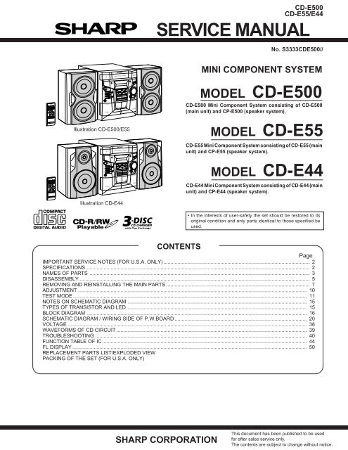
CD-E500CD-E55/E44<strong>SERVICE</strong> <strong>MANUAL</strong>No. S3333CDE500//Illustration CD-E500/E55MINI COMPONENT SYSTEMMODEL CD-E500CD-E500 Mini Component System consisting of CD-E500(main unit) and CP-E500 (speaker system).MODEL CD-E55CD-E55 Mini Component System consisting of CD-E55 (mainunit) and CP-E55 (speaker system).MODEL CD-E44CD-E44 Mini Component System consisting of CD-E44 (mainunit) and CP-E44 (speaker system).Illustration CD-E44• In the interests of user-safety the set should be restored to itsoriginal condition and only parts identical to those specified beused.CONTENTSPageIMPORTANT <strong>SERVICE</strong> NOTES (FOR U.S.A. ONLY) ....................................................................................................... 2SPECIFICATIONS ............................................................................................................................................................. 2NAMES OF PARTS ........................................................................................................................................................... 3DISASSEMBLY .................................................................................................................................................................. 5REMOVING AND REINSTALLING THE MAIN PARTS ..................................................................................................... 7ADJUSTMENT ................................................................................................................................................................. 10TEST MODE .................................................................................................................................................................... 11NOTES ON SCHEMATIC DIAGRAM .............................................................................................................................. 15TYPES OF TRANSISTOR AND LED............................................................................................................................... 15BLOCK DIAGRAM ........................................................................................................................................................... 16SCHEMATIC DIAGRAM / WIRING SIDE OF P.W.BOARD ............................................................................................. 20VOLTAGE ........................................................................................................................................................................ 38WAVEFORMS OF CD CIRCUIT ...................................................................................................................................... 39TROUBLESHOOTING ..................................................................................................................................................... 40FUNCTION TABLE OF IC................................................................................................................................................ 44FL DISPLAY ..................................................................................................................................................................... 50REPLACEMENT PARTS LIST/EXPLODED VIEWPACKING OF THE SET (FOR U.S.A. ONLY)SHARP CORPORATIONThis document has been published to be usedfor after sales service only.The contents are subject to change without notice.
CD-E500CD-E55/E44IMPORTANT <strong>SERVICE</strong> NOTES (FOR U.S.A. ONLY)BEFORE RETURNING THE AUDIO PRODUCT(Fire & Shock Hazard)Before returning the audio product to the user, perform thefollowing safety checks.1. Inspect all lead dress to make certain that leads are notpinched or that hardware is not lodged between the chassisand other metal parts in the audio product.2. Inspect all protective devices such as insulating materials,cabinet, terminal board, adjustment and compartment coversor shields, mechanical insulators etc.3. To be sure that no shock hazard exists, check for leakagecurrent in the following manner.* Plug the AC line cord directly into a 120 volt AC outlet.* Using two clip leads, connect a 1.5 kohm, 10 watt resistorparalleled by a 0.15 µF capacitor in series with all exposedmetal cabinet parts and a known earth ground, such asconduit or electrical ground connected to earth ground.* Use a VTVM or VOM with 1000 ohm per volt, or higher,sensitivity to measure the AC voltage drop across theresistor (See <strong>diagram</strong>).* Connect the resistor connection to all exposed metal partshaving a return path to the chassis (antenna, metal cabinet,screw heads, knobs and control shafts, escutcheon, etc.)and measure the AC voltage drop across the resistor.TO EXPOSEDMETAL PARTSVTVMAC SCALE1.5 kohms10 W0.15 µFTEST PROBECONNECT TOKNOWN EARTHGROUNDAll check must be repeated with the AC line cord plug connectionreversed.Any reading of 0.3 volt RMS (this corresponds to 0.2 milliamp.AC.) or more is excessive and indicates a potential shockhazard which must be corrected before returning the audioproduct to the owner.■ GeneralPower sourcePowerconsumptionDimensionsWeightFOR A COMPLETE DESCRIPTION OF THE OPERATION OF THIS UNIT, PLEASE REFERTO THE OPERATION <strong>MANUAL</strong>.AC 120 V, 60 Hz96 W■ Amplifier (Except for Canada)■ Amplifier (For Canada)Width: 10-5/8" (270 mm)Height: 12" (305 mm)Depth: 13-1/2" (342 mm)14.5 lbs. (6.6 kg)Output power 50 watts minimum RMS per channel into 8ohms from 100 Hz to 20 kHz, 10% total harmonicdistortionOutput terminals Speakers: 8 ohmsHeadphones: 16 - 50 ohms (recommended:32 ohms)Input terminalsOutput powerOutput terminalsInput terminals■ CD playerTypeSignal readoutD/A converterFrequencyresponseDynamic rangeVideo/Auxiliary (audio signal): 500 mV/47 kohmsRMS: 100 W (50 W + 50 W) (10 % T.H.D.)Speakers: 8 ohmsHeadphones: 16 - 50 ohms (recommended:32 ohms)Video/Auxiliary (audio signal): 500 mV/47 kohms3-disc multi-play compact disc playerNon-contact, 3-beam semiconductor laserpickup1-bit D/A converter20 - 20,000 Hz90 dB (1 kHz)Specifications for this model are subject to change withoutprior notice.SPECIFICATIONS■ TunerFrequency range■ Cassette deckFrequencyresponseSignal/noise ratioWow and flutter■ Speaker (CD-E500/E55)TypeMaximum inputpowerRated input powerImpedanceDimensionsWeight■ Speaker (CD-E44)TypeMaximum inputpowerRated input powerImpedanceDimensionsWeightFM: 87.5 - 108 MHzAM: 530 - 1,720 kHz125 - 8,000 Hz (normal tape)50 dB (TAPE 1, playback)50 dB (TAPE 2, recording/playback)0.3 % (WRMS)Twin-drive speaker system4" (10 cm) woofer 2100 W50 W8 ohmsWidth: 7-7/8" (200 mm)Height: 12" (305 mm)Depth: 7-1/16" (180 mm)5.7 lbs. (2.6 kg)/each2-way type speaker system2" (5 cm) tweeter5" (13 cm) woofer100 W50 W8 ohmsWidth: 7-7/8" (200 mm)Height: 12" (305 mm)Depth: 7-1/16" (180 mm)7.0 lbs. (3.2 kg)/each– 2 –
NAMES OF PARTSCD-E500CD-E55/E44■ Front panel1234567891011181922231213141516171. Disc Tray2. Timer Set Indicator3. Memory/Set Button4. Power On/Stand-by Button5. Clock Button6. Timer/Sleep Button7. Tuning and Time Up Button8. Tuning and Time Down Button9. Headphone Jack10. Tape 2 Record Pause Button11. Tape 1 Cassette Compartment12. Equalizer Mode Select Button13. Extra Bass/Demo Mode Button14. Volume Up and Down Buttons15. Disc Tray Open/Close Button16. Disc Skip Button17. Tape 2 Cassette Compartment18. CD Button19. Tape (1 2) Button20. CD or Tape Stop Button21. CD Track Down or Fast Reverse, Tape 2 Rewind,Tuner Preset Down Button22. Tuner (Band) Button23. Video/Auxiliary Button24. CD Play or Repeat, Tape Play Button25. CD Track Up or Fast Forward, Tape 2 Fast Forward,Tuner Preset Up Button20212425CD-E500/E551 2 3 4 5 6 710 11112 1389■ Display1. Disc Number Indicators2. CD Play Indicator3. Tape Play Indicator4. FM Stereo Mode Indicator5. FM Stereo Receiving Indicator6. Memory Indicator7. Extra Bass Indicator8. Timer Recording Indicator9. Timer Play Indicator10. CD Pause Indicator11. CD Repeat Play Indicator12. Tape Record Indicator13. Sleep Indicator■ Rear panel23451. Video/Auxiliary (Audio Signal) Input Jacks2. Cooling Fan3. AC Power Input Jack4. FM/AM Loop Antenna Jack5. Speaker TerminalsNote:This product is equipped with a cooling fan inside, which begins torun at a specified volume level for better heat radiation.1212■ Speaker system1. Woofers2. Bass Reflex Ducts3. Speaker Wire3– 3 –
CD-E500CD-E55/E44CD-E441 2 3 4 5 6 710 1112 1389■ Display1. Disc Number Indicators2. CD Play Indicator3. Tape Play Indicator4. FM Stereo Mode Indicator5. FM Stereo Receiving Indicator6. Memory Indicator7. Extra Bass Indicator8. Timer Recording Indicator9. Timer Play Indicator10. CD Pause Indicator11. CD Repeat Play Indicator12. Tape Record Indicator13. Sleep Indicator12345■ Rear panel1. Video/Auxiliary (Audio Signal) Input Jacks2. Cooling Fan3. AC Power Input Jack4. FM/AM Loop Antenna Jack5. Speaker TerminalsNote:This product is equipped with a cooling fan inside, which begins torun at a specified volume level for better heat radiation.1232■ Speaker system1. Tweeter2. Bass Reflex Ducts3. Woofer4. Speaker Wire4123456789101112131415161718192021■ Remote control1. Remote Control Transmitter2. Power On/Stand-by Button3. CD Button4. Tape (1 2) Button5. Memory Button6. Program Clear Button7. Tuning and Time Down Button8. CD Track Down or Fast Reverse, Tape 2 Rewind,Tuner Preset Down Button9. CD or Tape Stop Button10. Equalizer Mode Select Button11. Disc Number Select Buttons12. Tuner (Band) Button13. Video/Auxiliary Button14. CD Random Button15. CD Track Up or Fast Forward, Tape 2 Fast Forward,Tuner Preset Up Button16. Tuning and Time Up Button17. CD Play or Repeat, Tape Play Button18. Tape 2 Record Pause Button19. CD Pause Button20. Extra Bass Button21. Volume Up and Down ButtonsButtons with " " mark in the illustration or highlighted in bold on theright can be operated on the remote control only.– 4 –
Caution on DisassemblyFollow the below-mentioned notes when disassemblingthe unit and reassembling it, to keep it safe and ensureexcellent performance:1. Take cassette tape and compact disc out of the unit.2. Be sure to remove the power supply plug from the walloutlet before starting to disassemble the unit.3. Take off nylon bands or wire holders where they need tobe removed when disassembling the unit. After servicingthe unit, be sure to rearrange the leads where they werebefore disassembling.4. Take sufficient care on static electricity of integratedcircuits and other circuits when servicing.STEP REMOVAL PROCEDURE FIGURE1 Top Cabinet 1. Screw ...................... (A1) x5 5-12 Side Panel 1. Screw ...................... (B1) x8 5-1(Left/Right)3 CD Player Unit 1. Turn on the power supply, .. 5-2open the disc tray, take outthe CD tray cover, and close................................... (Note 1)2. CD Tray Cover ........ (C1) x13. Hook ........................ (C2) x24. Socket ..................... (C3) x15. Socket ..................... (C4) x2 6-14 Rear Panel 1. Screw ...................... (D1) x8 5-25 Main PWB 1. Screw ...................... (E1) x3 5-22. Screw ...................... (E2) x2 6-13. Socket ..................... (E3) x94. Socket ..................... (E4) x2 6-26 Front Panel 1. Screw ....................... (F1) x3 6-12. Hook ......................... (F2) x27 Display PWB 1. Screw .................... (G1) x13 6-28 Tape Mechanism 1. Open the cassette holder. 6-22. Screw...................... (H1) x89 Headphones PWB 1. Screw ....................... (J1) x1 6-210 CD Servo PWB 1. Screw ...................... (K1) x4 6-3(Note 2) 2. Socket ..................... (K2) x23. Solder ...................... (K3) x211 Turntable 1. Screw ....................... (L1) x1 6-42. Spacer ...................... (L2) x112 Loading Tray 1. Push forward the loading tray. 6-42. Inserting the flat head into thehole, push in the direction indicatedby the arrow. ... (M1) x213 CD Mechanism 1. Hook ........................ (N1) x2 6-5BlockNote 1: How to open the changer manually. (Fig. 5-3)1. In this state, turn fully the loading Gear in the arrow directionthrough the hold on the loading tray bottom.2. After that,push foward the loading tray.Note 2:1. After removing the connector for the optical pickup from theconnector, wrap the conductive aluminium foil around the front endof the connector so as to protect the optical pickup from electrostaticdamage.DISASSEMBLYSide Panel(Right)(B1)x2ø3x8mm(A1)x1ø3x8mmRearPanel(A1)x2ø3x16mm(B1)x4ø3x10mm(C2)x1Pull(C3)x1CD ServoPWB(D1)x6ø3x8mmLoading GearTop CabinetRear PanelFigure 5-1(D1)x2ø3x10mmFigure 5-2CD-E500CD-E55/E44FrontPanel(A1)x2ø3x16mmSide Panel(Left)(B1)x2ø3x8mmCD Player UnitCD Tray Cover(C1)x121Front SideorPull12(C2)x1(E1)x2ø3x6mmMainPWB(E1)x1ø3x10mmCD Player Unit(Bottom View)– 5 –Figure 5-3
CD-E500CD-E55/E44(C4)x2(E3)x4T/T Motor PWB(K1)x4ø3x8mm(F2)x1(E2)x2ø3x6mm(E3)x1Front Panel(K2)x1Switch PWB(K2)x1CD ServoPWBSolder(K3)x2(E3)x1Power PWBCD Player Unit(E3)x2(E3)x1Fan MotorPWBFigure 6-1Main PWB(F1)x3ø3x8mm(F2)x1(L1)x1ø3x10mmFigure 6-3(L2)x1Screwdriver(M1)x1Front Panel(E4)x2TurntableScrewdriver(M1)x1(G1)x13ø2.5x10mmLoading TrayDisplay PWBOpen(H1)x8ø3x8mmFigure 6-4HeadphonesPWB HolderPWB(J1)x1ø2.5x10mmCassetteHolderTapeMechanismCDMechanismBlockHook(N1)x1Figure 6-2PullHook(N1)x1PullCP-E500/E55/E44These speakers CP-E500,CP-E55,CP-E44 are available inassembles only and may not be disassembled.Figure 6-5– 6 –
REMOVING AND REINSTALLING THE MAIN PARTSTAPE MECHANISM SECTION(A1)x1(A1)x1ø2x3mmPerform steps 1 to 6 and 8 of the disassembly method toremove the tape mechanism.How to remove the record/playback and eraseheads (TAPE 1) (See Fig. 7-1)1. When you remove the screws (A1) x 2 pcs., the record/playback head can be removed.CD-E500CD-E55/E44ø2x7mm TAPE 1How to remove the playback head (TAPE 2)(See Fig. 7-2)1. When you remove the screws (B1) x 2 pcs., the erase headcan be removed.2. When you remove the screws (B2) x 2 pcs., the record/playback head can be removed.Note:After replacing the heads and performing the azimuthadjustment, be sure to apply screwlock.How to remove the pinch roller (TAPE 1,2)(See Fig. 7-3)1. When you remove the screw (C1) x 1 pc., the pinch rollercan be removed.Note:When installing the pinch roller, pay attention to the springmounting position.How to remove the motor (See Fig. 7-4)1. Remove the belt.2. Remove the screws (D1) x 4 pcs., to remove the motorbracket.3. Remove the screws (D2) x 3 pcs., to remove the motor.(B1)x2ø2x8mmRecord/Playback Head(B2)x1ø2x7mmErase HeadRecord/Playback HeadFigure 7-1(B2)x1ø2x3mmFigure 7-2TAPE 1 TAPE 2TAPE 2How to remove the belt (TAPE 1)(See Fig. 7-5)1. Remove the main belt (F1) x 1 pc., from the motor side.How to remove the belt (TAPE 2)(See Fig. 7-5)1. Remove the main belt (G1) x 1 pc., from the motor side.2. Remove the FF/REW belt (G2) x 1 pc.Pinch Roller(C1)x1Figure 7-3MotorPinch RollerPawl(D1)x2ø2x4mmMotorTAPE 2MainBelt(G1)x1TAPE 2Main Belt(G1)x1REW/FFClutch Ass'yTAPE 1Main Belt(F1)x1MotorTAPE 1(D1)x2ø2x4mmMotorBracket(D1)x3Special ScrewMotorBracketREW/FFBelt(G2)x1MainBelt(F1)x1MotorFigure 7-5– 7 –Figure 7-4
CD-E500CD-E55/E44How to remove the flywheel (TAPE 1,2)(See Fig. 8-1.)1. Remove the stop washer (H1) x 1 pc., with a small precisionscrewdriver to extract the flywheel from the capstan metal.Note:When the stop washer is deformed or damaged, replace itwith a new one.How to reinstall the partsInstall each part in the reverse order of the removal with care.TAPE 1TAPE 2MechanismChassisWasherx2Flywheel(H1)x1Stop WasherStopWasherDriverFigure 8-1How to remove the tape mechanism PWB(TAPE 1,2) (See Fig. 8-2.)1. Remove the screw (J1) x 1 pc., to remove the tapemechanism PWB.2. Remove the screw (J2) x 1 pc.3. Remove the solder joints (J3) x 2 pcs., to remove the tapemechanism PWB.TapeMechanismPWB(J1)x1ø2x3mmTAPE 1,2(J2)x1ø2x8mmTapeMechanismPWB(J3)x2SolderJointFigure 8-2– 8 –
CD PLAYER SECTIONPerform steps 1, 2, 3, 10,11, and 12 of the disassemblymethod to remove the CD mechanism.How to remove the T/T rotate motor(See Figs. 9-1)1. Remove the screws (A1) x 2 pcs.2. Remove the belt (A2) x 1 pc.3. Remove the screws (A3) x 2 pcs., to remove the T/T rotatemotor.Loading Tray(A2)x1(A1)x2ø2.4x3mmCD-E500CD-E55/E44(A3)x2ø3x10mmT/T Motor PWBLoading Tray(Bottom View)T/T Rotate MotorFigure 9-1How to remove the up/down loading motor(See Figs. 9-2)1. Remove the screws (B1) x 2 pcs.2. Remove the belt (B2) x 1 pc.Up/Down Loading Motor(B2)x1(B1)x2ø2.4x5mmCD Player UnitFigure 9-2HolderPWB(C1)x4ø2.5x10mmHow to remove the CD mechanism unit(See Fig. 9-3)Perform steps 1, 2, 3, 10and 13 of the disassembly method toremove the CD mechanism.1. Remove the screws (C1) x 4 pcs., to remove the mechanismunit.NoteAfter removing the connector for the optical pickup from theconnector wrap the conductive aluminium foil around the frontend of connector so as to protect the optical pickup fromelectrostatic damage.HolderCD Mechanism UnitFigure 9-3– 9 –
CD-E500CD-E55/E44MECHANISM SECTION• Driving Force CheckPlay: DM-300Torque MeterSpecified ValueTape 1: Over 80 gTape 2: Over 80 g• Torque CheckTorque MeterSpecified ValueTape 1Tape 2Play: DM-300 10 to 20 g.cm 10 to 20 g.cmFast forward: DM-300 — Over 50 g.cmRewind: DM-300 — Over 50 g.cm• Tape SpeedTest TapeAdjustingPointSpecifiedValueADJUSTMENTInstrumentConnectionTape TCC-119 Variable 3,000 ± 30 Hz Speakerspeed Resistor in Terminalmotor.(Loadresistance:8 ohms)TP302R356R357T351AM IFTAPE MECHANISMVariable Resistor in MotorFigure 10-1VR351FM MUTELevelT306T304FM IFAM BANDCOVERAGE fLTapeMotorIC30211 12L303FM BANDCOVERAGE fL112220IC301L302FM RFMAIN PWBR381TP301T302AM TRACKINGfLCNP301TUNER SECTIONfL: Low-range frequencyfH: High-range frequency• AM IF/RFSignal generator: 400 Hz, 30%, AM modulatedTest Stage Frequency FrequencyDisplay*1. Input: Antenna Output: TP302*2. Input: Antenna Output: TP301Setting/AdjustingPartsAM IF 450 kHz 1,720 kHz T351 *1AM Band — 530 kHz (fL): T306 *2Coverage1.1 ± 0.1 VAM Tracking 990 kHz 990 kHz (fL): T302 *1• FM RFSignal generator: 1 kHz, 40 kHz dev., FM modulatedTest Stage FrequencyFrequencyDisplaySetting/AdjustingPointFM Band — 87.50 MHz L303 (fL): *1Coverage1.3 V ± 0.1 VFM RF 98.00 MHz 98.00 MHz L302 *2(10-30 dB)*1. Input: Antenna Output: TP301*2. Input: Antenna Output: Speaker Terminal• FM IFSignal generator: 10.7 MHz, FM modulatedTest Stage FrequencyFrequencyDisplaySetting/AdjustingPointIF 10.7 MHz 98 MHz T304 *1(Turn thecore of transformerT304fully counterclockwise)*1. Input: Antenna Output: TP301• FM Mute Level (FM ST MODE)Signal generator: 1 kHz, 40 kHz dev., FM modulatedFrequencyDisplayAdjustingParts*1. Adjust so that an output signal appears.InstrumentConnectionInstrumentConnectionInstrumentConnectionInstrumentConnection98.00 MHz 98.00 MHz VR351*1 Input:CNP301(26 dBµV) Output: SpeakerTerminalFigure 10-2 ADJUSTMENT POINTS– 10 –
The test mode applied to this microcomputer has three modes,namely the ordinary test mode for adjustment or measurement,the aging test mode, and the self-diagnosis test mode for selfjudgmentin case of final product inspection.1. Turning on the test modeFor obtaining each test mode, press the POWER ON/STAND BY button, while keeping pressing the followingtwo buttons in the ordinary stand-by mode (power off ). Inthis case, the main unit buttons are valid. When turning thePOWER on with remote control buttons, test modes are notobtained.[Ordinary test mode]1. CD Test Mode (TEST 1) ..........................................CD + VOLUME UP2. Tuner Test Mode (TEST 2) ......................................TUNER(BAND) + VOLUME UP3. Electronic Volume Test Mode (TEST 3) ..................TUNING DOWN + VOLUME UP4. Timer Test Mode (TEST 4) ......................................TIMER/SLEEP + VOLUME DOWN5. FL Test Mode (TEST 5) ...........................................CLOCK + VOLUME DOWN6. CD MECHANISM Aging Test Mode (TEST 8) ........MEMORY/SET + VOLUME DOWNTEST MODECD-E500CD-E55/E44Press the following buttons in this state to obtain theoperations specified below."POWER ON/STAND BY" .. Test mode and power turned off toshift to the ordinary standby mode."FF/FWD" ................. After the pickup returns to theinnermost periphery, it slides towardthe outer periphery while this buttonis pressed."REW/REV" .............. After the pickup returns to theinnermost periphery, it slides towardthe inner periphery while this buttonis pressed. If PICKUP IN is on, inputis invalid."MEMORY/SET" ...... Shift to step 2"STOP" ..................... Invalid"VIDEO/AUX" ........... CLV2. Step 2 ModePress the "MEMORY/SET" button in this mode to transmitthe laser lighting command LDON (8400) and turn on thelaser. Any other operations are not performed in this case.[Self-diagnosis Test Mode]1. Button input diagnosis test mode (TEST06) .…....TUNNIG UP + VOLUME UPProcesses are different depending on destinations at initialsettings.2. CD Test Mode (TEST 1)In the CD test mode the operation of each step is possibleeven if the LID-SW is off. If focus cannot be taken in step3 or any error is processed, it is impossible to proceed tothe next step. During error processing, end the test modeby pressing the POWER ON/STAND BY button or return tothe step 1 by pressing the CD STOP button. Any otheroperations are inhibited.1. Step 1 ModeWhen the CD test mode is obtained, the following displaylights up. Then CD initialization operation flow proceedsup to CD STB off to wait for the following buttons to bepressed.Press the following buttons in this state to obtain theoperations specified below."POWER ON/STAND BY" . Test mode and power turned off toshift to the ordinary standby mode."FF/FWD" ................ The pickup slides toward the outerperiphery while this button is pressed."REW/REV" ............. The pickup slides toward the innerperiphery while this button is pressed.If PICKUP IN is on, input is invalid."MEMORY/SET"...... Shift to step 33. Step 3 ModeWhile the laser keeps lighting, CD initialization operationflow proceeds up to 'CLV servo ON' to wait for thefollowing buttons to be pressed.(Focus servo turned onfor focus search)The focus search is repeated to take focus.One second after display lights upPress the following buttons in this state to obtain theoperations specified below."POWER ON/STAND BY" . Test mode and power turned off toshift to the ordinary standby mode."FF/FWD" ................ The pickup slides toward the outerperiphery while this button is pressed."REW/REV" ............. The pickup slides toward the innerperiphery while this button is pressed.If PICKUP IN is on, input is invalid."MEMORY/SET"...... If focus has been taken, shift to step 4is executed. If not, acceptance isinhibited.*If the focus is not received after it has been taken, theprocess returns to step 1.– 11 –
CD-E500CD-E55/E444. Step 4 ModeThe CLV servo ON command (8600) is transmitted towait for the following buttons to be pressed. (The disc isrotated for CLV lock.)The time display always indicates "0:00".Press the following buttons in this state to obtain theoperations specified below."POWER ON/STAND BY" . Test mode and power turned off toshift to the ordinary standby mode."FF/FWD" ................ The pickup slides toward the outerperiphery while this button is pressed."REW/REV" ............. The pickup slides toward the innerperiphery while this button is pressed.If PICKUP IN is on, input is invalid."MEMORY/SET"...... Return to step 5*If the focus is not received, the process returns to step 1.5. Step 5 ModeWhen the CD initialization operation flow is completed,the mute is turned off, and playback is started. Even ifplayback reaches the outermost periphery of disc, theoperation does not stop. The LCD display indicates theplayback passage time as in case of ordinary CDplayback.3. Tuner Test Mode (TEST 2)1. Outline of tuner (radio) test modeThe tuner test mode is intended to store the adjustmentand measurement frequencies in the preset memoryCH. When adjusting the tuner section in the productionline, adjusting personnel are not required to set frequency.2. Details of tuner test modePress the "TUNER(BAND)" and "VOLUME UP" buttonsin POWER OFF state and turn on the power by the useof "POWER ON/STAND BY" button to preset and storefrequency for adjustment and measurement of destinationspecified by the AREA terminal in the preset memoryCH. However, Ordinary 1 and Ordinary 2 are stored inthe destinations when the test mode is obtained.(As for frequencies to be preset and stored for eachdestination, refer to item 3.)The tuner test mode is started from preset No.1.The operations of test mode are identical with the ordinaryoperations of TUNER function. FUNCTION switching isinvalid.It is necessary to discard the content of preset memorywhen the tuner test mode is ended; be sure to write "0000"or "1111" bits in the memory to be checked for judgingmemory error at initial setting and to initialize memory.When the tuner test mode is obtained, the following displaylights for one second.Press the following buttons in this state to obtain theoperations specified below."POWER ON/STAND BY" .. Test mode and power turned off toshift to the ordinary standby mode."FF/FWD" ................. The pickup slides toward the outerperiphery while this button is pressed."REW/REV" .............. The pickup slides toward the innerperiphery while this button is pressed.If PICKUP IN is on, input is invalid."PLAY" ..................... Invalid"STOP" ..................... Return to step 1*If the focus is not received, the process returns to step 1.Other cautions• TOC IL is not available for this test mode.• The TUNER TEST02 mode is obtained with >> + MEMORY/SET + POWER ON/STAND-BY. ->Turn off AC in the TEST02mode to restore the initial state.Turn off POWER to protect the memory of TEST02 mode.Turn off POWER again to obtain the ordinary operationwhile the data is stored in the memory (besides TUNER).If AC OFF state is maintained in this state for about 1/2 day,start is executed in the initial state.• To clear the whole memory, insert the AC cord, pressingMEMORY/SET + CD PLAY.– 12 –
3.Preset frequencies for various destinations(random preset memory)CH BANDFM1 FM 87.5 MHz2 FM108.0 MHz3 FM FM 98.0 MHz4 STEREO FM 90.0 MHz5 FM106.0 MHzCH BANDAM6 AM 530 kHz7 AM1720 kHz8 AM AM 990 kHz9 AM 600 kHz10 AM1400 kHzCH16-35BANDFM36 FM106.0 MHz37 FM 90.0 MHz38 FM FM 98.0 MHz39 MONO FM108.0 MHz40 FM 87.5 MHz• The slant line sections of the table store no memory.4. Electronic volume Test Mode (TEST 3)When this test mode is obtained, the following display lightsfor one second.CD-E500CD-E55/E445. Timer test Mode (TEST 4)When this test mode is obtained, the following display lightsfor one second.Set the current time and timer time according to the followingprocedure to reproduce the timer.1.Set the current time to 1:00, the timer to ON time 1:05, thefunction to CD, and volume to STEP 12, respectively. Oneminute is counted as one second, and the timer is reproduced.The fade-in (when playback is started) is executed at a rateof one step for 1 sec. After completion of fade-in, the fadeoutis executed at a rate of one step for 1 sec (WAIT 1 secinserted).After completion of fade-out, the power is turned off (afterWAIT 1 sec), and the mode is shifted to the standby.The display during operation is the same as that of ordinarytimer operation.6. FL Test Mode (TEST 5)When the FL test mode is obtained, all the FL segments arelighted. Then pressing the "PLAY" button switches displayas below.Lighting of all segmentsLighting of odd segmentsIn this mode, volume is Volume -14 dB (STEP23), FLATAND X-BASS ON, and start-up function to CD, respectively.The button operations in the test mode are the same asthose of ordinary operation except volume UP/DOWN.(1) The display is the same as that of ordinary operationexcept test mode setting.(2) Unlike the ordinary state, the volume is controlled withthe volume UP/DOWN button in accordance with thefollowing three steps.Lighting of even segmentsVolume- ∞ (STEP 0) Volume-14 dB (STEP 23) Volume-0 (STEP 30)(3) X-BASS is switched when button is pressed..– 13 –
CD-E500CD-E55/E447. Button input diagnosis Test Mode (TEST 6)When the test mode is obtained, the following is displayed.(STAND-BY AND DEMO OFF STATUS)8. CD MECHANISM Aging Test Mode (TEST 8)OPEN/CLOSE & 3 DISC CHANGER aging test.DISPLAY:This test mode is intended to check whether all the mainunit buttons can be detected. Accordingly, in this testmode, it is checked whether the "POWER ON/STAND BY"button was pressed after all the buttons shown below werepressed. If the result is OK, OK is displayed. If any one ofkeys was not pressed, an error is displayed. In both casesof OK termination or error termination, the mode is shiftedto the standby mode if the "POWER ON/STAND BY" buttonis pressed subsequently.All models using this type of microcomputer are not alwaysprovided with the same buttons. Since the buttons used aredifferent depending on models, types of buttons to be usedare determined by whether SURROUND, and an electric lidare available at the initial setting by MODEL port.The order of buttons to be pressed is not determined.Accordingly, it is checked whether all buttons have beenpressed.1. PU-IN buttons: REW/PRESET DOWN + CD STOPSince this model is provided with SURROUND (HAVEOR NOT), and electric CD lid, the following 10 buttonsare detected as all buttons.PLAY, X-BASS/DEMO, FUNCTION, VOLUME UP/DOWN, MEMORY/SET, REW, FF, STOP, CD-OPEN/CLOSEThe OK/NG display of test result is as follows.FUNCTION:Enter the TEST MODE 8, MCU control the 3 DISCCHANGER OPEN/CLOSE. After open finished, tray rotate1 circle (360 degree). Then close, After close finished, trayrotate 1 circle (360 degree) again.Request:Every period include 4 operation. Below is TIMING:Enter test modeCHANGERFind the disc 1 positionopendelay 3S after open finishrotate 1 circleclosedelay 3S after close finishrotate 1 circle– 14 –
• Resistor:To differentiate the units of resistors, such symbol as K andM are used: the symbol K means 1000 ohm and the symbolM means 1000 kohm and the resistor without any symbol isohm-type resistor. Besides, the one with “Fusible” is a fusetype.• Capacitor:To indicate the unit of capacitor, a symbol P is used: thissymbol P means pico-farad and the unit of the capacitorwithout such a symbol is microfarad. As to electrolyticcapacitor, the expression “capacitance/withstand voltage”is used.(CH), (TH), (RH), (UJ): Temperature compensation(ML): Mylar type(P.P.): Polypropylene type• Schematic <strong>diagram</strong> and Wiring Side of P.W.Board for thismodel are subject to change for improvement without priornotice.NOTES ON SCHEMATIC DIAGRAMCD-E500CD-E55/E44• The indicated voltage in each section is the one measuredby Digital Multimeter between such a section and the chassiswith no signal given.1. In the tuner section,indicates AMindicates FM stereo2. In the main section, a tape is being played back.3. In the deck section, a tape is being played back.4. In the power section, a tape is being played back.5. In the CD section, the CD is stopped.• Parts marked with “ 1 ” () are important formaintaining the safety of the set. Be sure to replace theseparts with specified ones for maintaining the safety andperformance of the set.REF. NO DESCRIPTION POSITIONSW1 PICKUP IN ON—OFFSW401 DISC UP/DOWN ON—OFFSW402 OPEN/CLOSE ON—OFFSW403 DISC NO. ON—OFFSW404 DISC 1 ON—OFFSW701 X-BASS/DEMO ON—OFFSW702 POWER ON/STAND-BY ON—OFFSW703 OPEN/CLOSE ON—OFFSW704 DISK SKIP ON—OFFSW705 VIDEO/AUX ON—OFFSW706 TAPE ON—OFFSW707 PRESET DOWN ON—OFFSW708 PLAY/REPEAT ON—OFFSW709 PRESET UP ON—OFFSW710 STOP ON—OFFREF. NO DESCRIPTION POSITIONSW711 MEMORY/SET ON—OFFSW712 TUNING/TIME DOWN ON—OFFSW713 TUNING/TIME UP ON—OFFSW714 TIMER/SLEEP ON—OFFSW715 CLOCK ON—OFFSW719 EQUALIZER ON—OFFSW720 VOLUME UP ON—OFFSW721 VOLUME DOWN ON—OFFSW722 TUNER(BAND) ON—OFFSW723 CD ON—OFFSW724 REC/PAUSE ON—OFFSW801 TAPE2 INITIALIZE ON—OFFSW802 TAPE1 INITIALIZE ON—OFFSW803 TAPE2 REC ON—OFFTYPES OF TRANSISTOR AND LEDFRONTVIEWE C B(S) (G) (D)(1) (2) (3)HSB562 CHSC1609 GRKRA102 MKRA107 MKRC102 MKRC104 MKRC107 MKSA1015 GRKSA1271 YKSC1815 GRKSC3203 YSSC1674 C2SC2001 K1 2 3KDV147BSVC348S– 15 –
CD-E500CD-E55/E44AM LOOPANTENNAFMANTENNA321CNP301B.P.FBF301AM TRACKINGT3021FM RFL302FMOSCFM IFT3046IC301TA7358APFM FRONT END2 3 4 5 7 8T3069L303OSC BUFFQ302AM BANDCOVERAGEFM IFCF303IC303LA1832SFM IF DET./FM MPX./AM IFFM MUTELEVELVR351FM OSCQ306AM OSCOUTCF302AM OSC INAM RF INIF OUTDZH05C2+CF351 X351T351 CF352456 kHz1 2AM IF4 5 9 8 17 13AM MIX AM IF GND FM MO/STVCC DET VCO LIC30314FM/AMRLA1832S15OUT MPXINFM/AM24 23 21 10 7 6 18 16 12STEREOSDQ351SWITCHINGSD+B2CNP2027FM ST6CE5FRODISPLAYCNSCL4DO3DI2VTX3524.5 MHzFM INAM INFROMCD SECTIONCNS205TAPE 2L-CHR-CHP.B ṚECL-CHR-CHTAPE 2ERASEHEAD20 1 22 16 15 11CNP2053 4 5 6OSCLIC3021LC72131PLL(TUNER)172FM/AM MO/STR3 7 9 10 21 8TAPE 1PLAYBACKHEADRECORD/PLAYBACK HEADSW801INITIALIZESW803RECSOL801SOLENOIDPHOTE INTERRUPTERTAPE 1SW802INITIALIZESWITCHING+B2Q801Q803Q821Q822Q823BIAS CONTSWITCHINGSWITCHINGQ820SWITCHINGQ807,Q808Q813,Q814Q802Q810Q811Q809L(T1)R(T1)L(T2) 2R(T2) 23L NFR NFSWITCHINGU_CON5VFML REC 9 RECR REC 16REF 14SWITCHING124322615 12 11M801TAPEMOTOR+B3Q360SWITCHINGP.B19M134 L21 R520718FMPBL RECR8 L NF17 R NF10 ALC+B2Q812Q819CEDICLDOIC801AN7345KPLAYBACK AND RECORD/PLAYBACK AMP.+B2Q815Q804+B2TAPE MPTORDRIVERSOLENOIDDRIVERQ818Q817MUTECNP803TAPE_SW1T2_RUN_PLUS2T2_SOL3T1_SOL4T1_RUN_PLUS5CH_SW6T_MOTOR7BIAS8REC/PLAY9REC10CNS803FROMDISPLAY SECTIONCNS901AUXTAPELRTUNER LRCDLRLR+++VV–+DGSOL802SOLENOIDPHOTE INTERRUPTERQ806Q805SOLENOIDDRIVERQ816+Figure 16 BLOCK DIAGRAM (1/4)– 16 –
CD-E500CD-E55/E44FROMDISPLAY SECTIONCNS202FROMCD SECTIONCNS204202 CNP2045 4 3 2 11 2 3 4 5 6CECLDODIDODICLM_GND+7VD_GND+B4CNP102CD_+B1MUTE2SIGAL_LVL3SP_RLY4SP_DETECT5FAN_START6FAN_PRT7FROMDISPLAY SECTIONCNS102D_GND+B5FAN MOTORDRIVERQ201,202Q204,205MM101FANMOTORSO601VIDEO/AUX INSYSTEMMUTEQ101Q102Q105Q106Q203Q108Q109+B3SO101SPEAKERTERMINALAUX L 9R 16TAPE L 10R 15TUNER L 11R 14CD L 12R 13IC601LC75341MDICECLAUDIO PROCESSOR 2147 8 17 18 3 231224RLL 15R 1IC101STK40207POWER AMP.PRE+VCC4+VCC8–VCC9PRE–VCC126R-OUT710 L-OUT11Q103Q104RLY101+B2Q107JK101HEADPHONES+B2Q208+B1–B1F9015A/125V+B2FROMDISPLAY SECTIONCNS901+B4+B5A_12V+B2VF1VF2–B2+B3DGND+B3CD+BCNP90112345CD_7V+5.6 V–30 V+5.6 VQ207VOLTAGEREGULATORVF2VF1Q206IC203KIA7808APIVOLTAGEREGULATORIC202KIA7812APIVOLTAGEREGULATORIC201KIA7805APIVOLTAGEREGULATORD905~D908D901~D904Q901F9025A/125VF9031.6A/125VVOLTAGEREGULATORT901POWER TRANSFORMERAC POWERSUPPLY CORDAC 120 V,60 HzFigure 17 BLOCK DIAGRAM (2/4)– 17 –
CD-E500CD-E55/E44TO MAIN SECTIONR-CHAGNDL-CHDGND+7V (+B5)MGNDCLDIDOVWRQDRFCD RESCEROTATECLOSE_SWDISC 1_SWDISC NO._SWOPEN_SWDOWN_SWUP_SWCNS2053 21 6 5 43 2 1CNS204CNP40511 10 9 8 7 6 5 4 3 2 1SW401DISCUP/DOWNSW402OPEN/CLOSEQ412CONSTANTVOLTAGESW403DISC NO.SW404DISC 1756957565545 42 68 41 46 64 63 62 67 66 65 61RCHOLCHOVDD5LVDDRVDDDODICLDRFRESVWRQCE+7VQ401,402Q403,404Q405,406Q407,408+–M–MM402ROTATEMOTOR51504443403728196IC401LC78646ESERVO/SIGNAL CONTROL+M401UP/DOWN LOADINGMOTORXL40116.9344 MHz48 XOUT49 XINRFVDDADAVDDVDDXVDD5+3.3VVVDDVREFFIN1 AFIN2 BTIN1 ETIN2 F18 38 47 77 11 7 8 9 10LDSLDD79 80CONT4 25CONT5 26SLDO 23SPDO 22FDO 21TDO 20+7V2 MUTE4121927130VCCVCCIC402LA6548DFOCUS/TRACKING/SPIN/SLEDDRIVER24~229~7+3.3VCONSTANTVOLTAGEQ411LASERDRIVER29 VREFREG_INREG_OUT25 26 20 21 15 14 6 5 11 10Q409+3.3V+3.3VVCCVCECABCFLDMD+5VFOCUS COILTRACKING COILCD PICKUP UNITNM802SPINDLEMOTORNM801SLEDMOTORMM+––+SW1PICKUP INFigure 18 BLOCK DIAGRAM (3/4)– 18 –
CD-E500CD-E55/E44VFD701FL DISPLAYTO POWER SECTIONCNS9013.8VVF1 1VF2 23.8V–B2 3–30V+B3 45.6VD_GND 5VF233 3231 ~ 16+B315 ~ 1211 ~ 3VF12 1Q701LED701CNS405UP_SW 170 DISC_UP_SW67 ~ 52~P20P551 50 ~ 4738 ~ 30~~GNDP4P1G1G91IRQ 29REMOTESENSORRX701+B3DOWN_SW274 DISC_DOWN_SWOPEN_SWDISC NO._SWDISC 1_SWCLOSE_SWROTATECE34567875 OPEN_SW68 DISC_NO_SW69 DISC1_SW71 CLOSE_SW73 ROTATE4 CD_CEPOWER_KEY 28X-BASS/DEMO 27SW702POWERON/STAND-BYSW701X-BASS/DEMOCD RES95CD_RESDRF 10VWRQ 11CNS803TAPE_SW 1T2_RUN_PLUS 26 CD_DRF7 CD_WRQ89 GND23 T2_TAPE2_SW83 T1_RUN_PLUSIC701IX0058SJSYSTEMMICROCOMPUTERKEY2_IN 19KEY1_IN 18CF2 16KEYSW703~SW710SW719~SW721KEYSW711~SW715SW722~SW724T2_SOLT1_SOL3481 T2_SOL80 T1_SOLCF1 15X7028 MHzT1_RUN_PLUSCH_SW5682 T1_RUN_PLUS84 CH_SWGND 14MOTOR779 MOTORTAPE_BIASREC_PLAY8976 TAPE_BIAS77 REC_PLAYVDD1 17REC SW1078 RECFAN_PRTFAN_STARTSP_DETECTSP_RELAYSIGAL_LVLP_MUTECD+BD1D0CLCEFM_STSDRESET IN PUTSYS_STOPVDD2 90VDD3 46VDD4 72+B3CNS10221 92 93 94 91 88 85 95 96 97 98 99 10011 26TO MAIN SECTIONFAN_PRTFAN_STARTSP_DETECTSP_RELAYSIGAL_LVLP_MUTE765432CD+B1RESETQ702,Q703,Q704CNS202D_GNDD1D0CLCEFM_STSD1234567Figure 19 BLOCK DIAGRAM (4/4)– 19 –
CD-E500CD-E55/E44ABFM SIGNALAM SIGNALAM TRACKINGT302C33012P(CH)C3310.047C3320.022+BFM MUTELEVEL10K(B)VR351R358L351µC3290.022D3011N4148VD301SVC348S+BCD3021N4148C3370.022AM OSC.T306C335560PR32368KC33427P(UJ)R3365.6KR3515.6KAM BANDCOVERAGE fL2.1VC3510.022DIC301FM FRONT ENDTA7358APCFFMBAND PASSFILTER0.8V11.5V25.2V31.5V40V55.2V64.4V73.8V85.2V9BF301EFFMANTENNAAM LOOPANTENNA123AM1GND2FM3CNP301C3020.001C3010.012D3071N41481 2 3D3051N4148C3040.01C31918P(CH)D3061N4148C3050.0047C3069P(UJ)C3070.0047L302FM RFC3080.022C3185PC3030.001R302100KC3090.001R30122C3200.001VD303KDV147BR30333KT304FM IFC31110P(CH)R30447KQ302SSC1674 CR30747R31533FM OSC.FM BANDCOVERAGE fLC315100PL303R30633C31233PC3136P(UJ)R305680C31422P(CH)C31610/161FM IFCF3032R30810K3VD302KDV147B+BC3170.022+BR313680R314R31633 330R3122.2KQ306SSC1674 CR309470+CHASSISGNDC3490.001C3210.0033R3104.7KGH• NOTES ON SCHEMATIC DIAGRAM can be found on page 15.1 2 3 4 5 6Figure 20 SCHEMATIC DIAGRAM (1/11)– 20 –
CD-E500CD-E55/E44MAIN PWB-A (1/3)FM MUTELEVELC3740.022+B10K(B)VR351R3588.2KL3531µHC34333PC3623.3/50C3600.022C3610.022C3630.022C36410/16C3650.022C3660.001R3502.7KC3671/50X351456 kHzTP302R357470KR3561KC3681/50C36956PC3730.022R3643.3KR3633.3KQ3511 KRC104 M4.7V 23(0V)C371 R3611/50 12KR36212KC3721/502.5V5V2.1V(2.7V)2.1V(2.7V)0.6V0V(0.9V)2.3V(0V)2.3V2.1V1.3V1.3V4V(2.2V)24 23 22 21 20 19 18 17 16 15 14 13R3365.6KR3515.6KAM OSCOUTFM IF INAM MIX OUTAM OSCINREGFM AFCAM RFINVSMIC303LA1832SAM IF INCUTAM LOW2.1V2.1V5V2.1V0V5V5V2.9V(4.3V)5V0V3.8V(1.9V)C3581/503.8V(1.2V)CF302 2C344FM IF33P+BT351C378 AM IF330P+BR37610KL352100µHZD351DZH05C2++BC3830.022GNDFM/AMOUTSDSTEREOFM DETMPX VCOVCCMPX INIF OUTR-CHOUTPHASEL-CHOUTMO/STPHASE(AM/FM)R3662.2K123FM IF DET./FM MPX./AM IFR3521K456789101112C3510.02213C35210/16C3500.022CF35213C3530.022C3540.022CF351R353270C3990.022C398100/10C3560.001C3572.2/50R3553.3K2FM IFC35522PC3701/50R3931KR39547K1SD2FM ST3DOR309470+BR382330R386330C38112P(CH)X3524.5 MHzC38215P(CH)C3840.001C3970.022X OUTX INVT2.6VTP301VSS2.6V0VC39447/16R38110K0.1VR3741K0.1VC3920.001C393 R3801/50 1.5K0.9VIC302LC72131PLL(TUNER)AOUTCEAIN4.8VC38010/165.1V0.9VDICLDOPDR3731KR3721KR3711KR3792.2KC3870.0221.7V+BFM(11.4V)5.2V2.6V(0V)VDDFM INMUTE3.7V(0V)0V(2.6V)AM IN3.9VFMR3775.6KL351100µHC3850.0122 21 20 19 18 17 16 15 14 13 12123456789MO/ST103.5V(0V)IF REQ I F INR3591.8KR3604.7K0V11C386330PR36510KR3875.6KC396100/10+BR391 C395390 0.022R392390Q360KSA1015 GR+B 10VR3835.6KR3855.6KR3846.8KD3081N41489.3V9.3VC39147/16+B4 CL5 CE6 DI7 A_12V8 D_GND9 TUN_L10 TUN_R11 A_GNDTO MAIN PWB (3/3)MAIN SECTIONP24 1 - C+B7 8 9 10 11 12Figure 21 SCHEMATIC DIAGRAM (2/11)– 21 –
CD-E500CD-E55/E44ABCDEFGHTAPE MECHANISM ASS'Y(219)TAPE 2R-CHL-CHR-CHL-CHSOL801 (219-5)SOLENOIDTAPE 1PLAYBACK HEAD (219-7)TAPE 2RECORD/PLAYBACK HEAD (219-7)M801 (219-10)TAPEMOTOR+CN1–MERASE HERD (219-6)PHOTOINTERRUPTERSW801 (219-8)INITIALIZESW803 (219-9)REC1231234567123456TAPE MECHANISM PWB-H1,2 (219-11)TAPE 1SOL802 (219-5)SOLENOIDPHOTOINTERRUPTERSW802 (219-8)INITIALIZECNW801CNW802TAPE MECHANISM PWB-H1,2 (219-11)712345671234567CNS8041234567CNS805123123456712345671234567CNP801C801MAIN PWB-A(2/3)Q801KSC1815 GR560PCNP802CNW804R86418KR86533KCNW805PLAYBACK SIGNALRECORD SIGNALC802560PR802270TI_RA_GNDT1_LR803270R80547KR806Q802KSA1015 GRR80447KC803560PC804560PR80947K4.7K 4.7K1N4148 1N4148R8183.3KR8192.2K2.2KQ803KSC1815 GR3.3KQ808KSC1815 GRR817150Q813KSC1815 GRQ814KSC1815 GRQ807KSC1815 GRC807 1 Q8093.3/50 KRC107 MQ804HSB562 CR82710KC810 C80982P82PR81110KQ810C805KRC104 MR8330.022 10K2 3R81510K 1R846R816 2 310K4.7KQ811KRC104 MD802R80747KR810D801C8063.3/50R812R8133123 2Q806KRC107 MC849100/10R82510KR82056KQ805HSB562 CR82810KR8291KR8301KR8321KR8311KR8221.5K+BR826R8231.5KR82156K10KL(T1) R(T1)C808R837 100/25C817100/25R836100/25 47 C81847L(T2) R(T2)24C815330P1 2C814330P2K• NOTES ON SCHEMATIC DIAGRAM can be found on page 15.1 2 3 4 5 6Figure 22 SCHEMATIC DIAGRAM (3/11)– 22 –
CD-E500CD-E55/E44R82410KQ812KSC1815 GRR85147KR82810KR8291KR8301KR8321KC817100/25R83647C815330PC812330PC821R84233KC8230.033R838100K560PR8403.9KC8270.0022R848R8445.6KC82547/25R8473.9K6.8KC8320.001R8521.5KC836 R8540.022 100C83422/50C84047/25R85710KC8380.0033C84222/50C843220/16+BC8440.022+BR859220+B+BTAPE LTAPE RREC LREC RVCC_12VM_GNDA_GNDM_12Vµ_CON5V121314151617181920TO MAIN PWB(3/3)AMP. SECTIONP24 6 - AC810 C80982P82PL:T1H:T2R8311K24R(T1)L(T1)C814330P100/25C818R8374723IC801AN7345KPLAYBACK and RECORD/PLAYBACK Amp.R(T2)L(T2)1 2 3 4 5 6 7 8 9 10 11 12C816330P22R NFL NFC822560PR839100KR841C8240.033R84333K21PROPLO3.9K20C82647/25R8455.6KR849C8280.002219R8503.9K18RRIRLI6.8KC8330.001R8531.5K17R NFL NFC83522/50R855 C837100 0.02216RRORLOC84147/25C8390.0033R85810K15ALC14REFC8293.3/5013VCCC8300.022Q821KRC104 M312R86247K+BR8604.7KR86147KC8450.0022C8460.027(ML)Q822KSA1015 GRR863100KR866100C847100/16Q8232SC2001 KL801330µHR83310KC850330/16R84610K Q819KSC1815 GRR8221.5KR82056KR82610KC808100/25D8031N4148Q815HSB562 C+BR8351.5KR83410K 21D8041N41483Q817KRC102 MC8200.02221R85647KD8051N41483 Q818 3KRC102 M1+BC831 Q8200.022 KRA102 M 2+BJ213ThermistorRECREC/PLAYBIAST_MOTORCH_SWT1_RUN_PLUST1_SOLT2_SOLT2_RUN_PLUSTAPE_SWCNP80310987654321FROMDISPLAY PWBCNS803P28 1 - C805562 CR8231.5KR82156K+B21Q816KRC102 M3C8190.0227 8 9 10 11 12Figure 23 SCHEMATIC DIAGRAM (4/11)– 23 –
CD-E500CD-E55/E44FROM DISPLAY PWBCNS202P28 1 - EFROM CD SERVO PWB CNS204P27 11 - CTO MAIN PWB(2/3)TAPE SECTIONP23 12 - BACNP2027 6 5 4 3 2 1 1 2 3 4 5 6CNP204SDFM_STCECLDODID_GNGDODICLBCR20110D2101N4004D2071N4004C201100/16C2020.022R1011KR1021KM_GND+7VD_GND+B20 19 18 17 16 15 14 13 12µ_CON5VM_12VA_GNDM_GNDVCC_12V+B+B+BREC RREC LTAPE RTAPE LTO MAIN PWB(1/3)TUNER SECTIONP21 12 - ESD1FM ST2DO3CL4CE5DI6A_12V7D_GND8TUN_L9TUN_R10A_GND11+BFM SIGNALCD SIGNALPLAYBACK SIGNALRECORD SIGNALAUX SIGNAL+B+BIN1DETO POWER PWBP37 12 - BCNP201CNS2011234567CHASSISGND12345678CNW201+B1+BA_GND1–B1 –BD_GND+B2 +BD_GND+5.6V+BA_GND1+B1–B1+BC2033300/35C2074700/50C8510.0047C2064700/50C2080.022+BIC203KIA7808APIVOLTAGEREGULATOR123C209470/16R21710K+BC2100.022–BA GND+BQ101C101 KSC1815 GR33/16R1066.8KR1053.3KR10310KQ102KSC1815 GRR10410K C119220PR1271KC120220PR1281K1C1050.0015R1091KR10739KC1031/50V–BFIC202KIA7812APIVOLTAGEREGULATOR+B +B13+BQ206HSB562 C+B+B2C2040.022+BC205220/25IC201KIA7805APIVOLTAGEREGULATOR13+BR218560Q207KSC1815 GRR2191KGD2011N40042C2110.047C21247/25+B+BR202Q20HSC1609H• NOTES ON SCHEMATIC DIAGRAM can be found on page 15.1 2 3 4 5 6Figure 24 SCHEMATIC DIAGRAM (5/11)– 24 –
CD-E500CD-E55/E44O MAIN PWB(2/3)APE SECTIONP23 12 - BCNS205FROM CD SERVO PWBP27 11 - D_8 17 16 15 14 13 12M_GNDVCC_12V+BREC RREC LTAPE RTAPE L1 2 3CD_LA_GNDCD_RCNP205R61833KR616 R62033K 3.9KR624C60612K 10/16R62512KTAPE LTUN LCD LCD RTUN RTAPE RC60410/16C60510/16R6041KC62410/16R1 L1R607R6061K R2L21KR609R6081K R3L31KR629R6281K R4L4 1KC608C6074.7/50RSL0LSL04.7/50C610 RIN LINC6092.2/502.2/50C612 R6130.0027 RTREC611LTREC6140.0027 R6123.9K 0.1 RBSC613 3.9KLBS(CH)0.1(CH)C61733/16 C622C623ROUT LOUT0.10.1 C616 VREFC6152.2/16VSS2.2/16VDD CEC618100/16CL DIIC601 12 11 10 9 8 7 6 5 4 3 2 1LC75341MAUDIOPROCESSOR13 14 15 16 17 18 19 20 21 22 23 24C60110/16C60310/16C60210/16R6051KR6021KR603R617 R621AUX R1K33K 3.9KC62510/16R61933KB +BR630220RR6011KR61410KR61510KCLCEDIR622100KAUX LLMAIN PWB-A(3/3)R623100KC619220PC620220PC621220PCNP601R643 R6412.2K 22KR644 R6422.2K 22K123CNS601123123TERMINAL PWB-B4L6012.2µHCNW601D6041N4148CHASSISGNDD6051N4148L-CHR-CHSO601VIDEO/AUX INR1011K01GR2R200PR1021KIN1C1050.0015R1091KR10739KC1031/50VNF1N.C.R1131KR111470C10710/50PRE+VCC100/50R13222KR117100R11556KC1093P(CH)BIAS+VE1–VE1R1190.20(1W) R1214.7KC1170.022R1234.7KQ103KSC1815 GR D1011N4148 +BIC101STK40207POWER AMP.+VCCC113 C1140.022 0.022+BC111 C11210/50 10/50–B–VCC+VE2–VE2R1200.20(1W)C116100/50R118100R11656KC1103P(CH)R1224.7KC1180.022R1244.7K Q104KSC1815 GRPRE–VCC1 2 3 4 5 6 7 8 9 10 11 12 13 14 15C115D1021N4148GNDR1141KR112470NF2C1350.022C10810/50R1356.8R1366.8C1330.022IN2C1060.0015R1101KR10839KC1041/50VC1340.022D1041N4004C1360.022RLY101RERAYR13147KR221220ZD201DZH05C2+Q208KSC1815 GRQ107KSC1815 GRC1260.1C1280.1R1374.7C1460.0047C1450.0047R1384.7C1270.1C1250.1L1052.2µHCNP101R INR OUTA_GNDL OUTL INSO101SPEAKERTERMINAL+L-CH–+R-CH–12345CHASSISGND12345CNS101CNW101R IN12345R OUTA_GNDL OUTL INL10310µHR127A390R128A390HEADPHONES PWB-B332145910JK101HEADPHONES+B +BD1031N4148Q106KSC1815 GRR12556KR12656KR20610K1Q109KRC107 M2 3 23Q1081KRA107 MC1210.001C1023.3/16Q105KSC1815 GRC13047/50R20818KR1305.6KD2031N4004 R212100KQ203KSC1815 GRD2051N4004R209100KD2041N4004FAN_PRTFAN_STARTSP_DETECTSP_RLYSIGAL_LVL+BMUTECD+B7654321CNP102FROMDISPLAY PWBCNS102P28 1 - D+BR20222KQ201HSC1609 GRR20522KR203 D2023.3K 1N4004R204 C21310K 47/16R207470KQ202SSC1674 C+BQ204KSA1015 GRC21410/16R21127KQ205KSC1815 GRR2133.3KR21056CNP203 CNS2033 32 21 1MM101(204-4)FAN MOTOR7 8 9 10 11 12Figure 25 SCHEMATIC DIAGRAM (6/11)– 25 –
CD-E500CD-E55/E44ACD SERVO PWB-CCD SIGNALBCD PLAYER UNIT ASS'Y (238)+BC421100/10C420.1CD MECHANISM UNIT ASS'Y(238-1)+BR41547L4010.82µHCMDLDFO–TR–TR+FO+ACTUATORVRSHORTLANDFCBAFO–16TR–15TR+14FO+13MD12VRLD10GND98FCBACEVCC765432VC111 1110FC401FO–16TR–15TR+14FO+13PD12VRLD987GNDFCB6A5D4E321VCCVCCNP401R401R402R403R404R405R406R451100100K33K33K33K33K100KC401 C4020.01 47/25C4030.01R4173.3Q409KSA1015 GRC4070.01C40647/25C40847/25+BL4020.82µHR41927KC4090.1C410100/10C4140.047C4150.1R42110KC416 R420 C422100P 330 0.002C417100/10C41910/50DCECD PICKUP UNIT+BC4120.1C411100/10C4201/50C41847PL4030.82µHC4250.002ADAVSSTDO2R41612KL4040.82µHEC4041/1016 17 18 19 20 21 22 23 24 25 26 27 28 29 30+BNM802SPINDLEMOTORNM801SLEDMOTORSW1PICKUP INMM+–+–CNS402SP+6 6 7SP–5 5 6SL+4 4 5SL–3 3 4PU-IN2 2 31 1 2GND1CNW402SP+SP–SL+SL–PU-IND_GNDREG_IN RESETREG_OUTCDVIN2 VIN3VG2 VG3VO2+ VO3+VO2–VO3–GNDGNDGNDGNDVO4–GNDGNDVO1–VO1+ VO4+VG1 VG4VIN1 VIN4MUTE VREFVCC VCCIC402LA6548DFOCUS/TRACKING/SPIN/SLED DRIVER15 14 1312 11 10 98 7 6 5 4 3 2 1F+BR418100KM401 (238-2)UP/DOWNLOADING MMOTOR+–R453M+ 6812M–3CNW404C405330/10+BGQ401KSC3203 YR407 R4091.5K 22KR4083.3KQ402KSA1271 YQ403KSC1815 GRR41022KQ404Q407KSC1815 GRKSC1815 GRQ405KSA1271 YQ406KSC3203 Y R414470Q408KSA1271 Y+B +B+BR4113.3KL4100.82µH+BR412R4131.5K3.3KQ411HSB562 CD405D402D4011N40041N40041N4004+BH• NOTES ON SCHEMATIC DIAGRAM can be found on page 15.• The numbers 1 to 12 are waveform numbers shown in page 39.1 2 3 4 5 6Figure 26 SCHEMATIC DIAGRAM (7/11)– 26 –
CD-E500CD-E55/E44C428100PC429100PC430100PC431100PC432100PC4330.022+BR4351KR4361KR4371KR4381KR4391KR440100R4411KDODICLCECNP405VWRQ11DRF10CD_RES9CD_CE8ROTATE7CLOSE_SW6DISC1_SW5DISC NO_SW4OPEN_SW3DOWN_SW2CNS405P28 4 - HFROM DISPLAY PWBC4230.1R4241.2K+BC4260.1R42612KR429680C4271/50C4340.047R43410KL4070.82µHL4090.82µHUP_SW1SW401DISCUP/DOWN+B+BR42110K1LDDLDSR42210KR4236.8KR42515KR4271KR4281KR43068080 79 78 77 76 75 74 73 72 71 70 69 68 67 66 65 64 63 62 61SLCOSLCISTEFMINRFFRVVDDPCKISTVVSSPD02PD012DATACK3LRSY20 C4224ASDFIN30 0.00225 RFVDD 5 8 7 3ASDACK 56C4426 RSVSSASRACK 5510P(CH)7 FIN1 AIGMOUT 54 L4068 FIN2 BEFLG 53 0.82µH9 TIN1 EC2F 52C44710 TIN2 FIC401XVSS 51 0.0195011 VREFLC78646EFSX/16MIN 50R443100 C44312 REF1 SERVO/SIGNAL CONTROL XIN 4910P(CH)13 FEXOUT 4814 TECXVDD 47015 TE4RVDD 46R4470100C425 16 RFMONRCHO 450.0022ZD40117 JITTCRVSS 4469DZH03C3+18 ADAVDDLVSS 43ADAVSS19 LCHOC44142TDO0.0222041LVDDC4392 21 22 23 24 25 26 27 28 29 30 31 32 33 34 35 36 37 38 39 40 C437 330/6.3030.01µH 1C43810/50R4422.2K C4400.0015FDOSPDOSLDOGPDACCONT4CONT5CONT2CONT3VSSVDD5DRFVRESVWRQDODICLCESBCK/FGDEFECTV/1PFSEQMON11MON12MON13MON14MON15VSSVDDDOUTTESTR43110KC4350.1+BDATA60595857C436100/10121110R44610KX40116.9344MHZL4120.82µH+BC44510/50R4492.2KC4440.0015R44810K+BL4050.82µHC4480.022Q412KSC3203 Y+BC44947/16R452220ZD402DZH06B2+L4110.82µH+BCNW204DO1DI3CL4MGND5+7V6DGND7L-CHAGNDR-CHCNW205212CNP406OPEN_SW3DGND2CLOSE_SW1MR401CORE5CD PLAYER UNIT ASS'Y(238)321321CNS20412346123 3CNS205CNP204TO MAIN PWB(3/3)P24 5 - ACNP205TO MAIN PWB(3/3)P25 7 - ASWITCH PWB-GSW402 (238-4)OPEN/CLOSET/T MOTORPWB-F+B+BL4080.82µH+BDISC NO_SW12DISC1_SW3MGND4ROTATE+5DGND61234512345SW403 (238-5)DISC NO.SW404 (238-6)DISC 1+– MCNW403CNS403M402 (238-3)ROTATEMOTOR+B+B7 8 9 10 11 12Figure 27 SCHEMATIC DIAGRAM (8/11)– 27 –
CD-E500CD-E55/E44ADISPLAY PWB-B2VFDFL DBCDECNP901 TO POWER PWBP37 12 - DCNP803 TO MAIN PWB(2/3)P23 12 - FCNP102 TO MAIN PWB(3/3)P25 11 - GCNP202 TO MAIN PWB(3/3)P24 2 - ACNS90112345CNS803123456789107654321CNS1021234567CNS202CNW90113.8V VF12VF23.8V –B3–30V455.6V +BD_GND6CNW803TAPE_SW12345678910118765432112345678T2_RUN_PLUST2_SOLT1_SOLT1_RUN_PLUSCH_SWMOTORTAPE_BIASREC_PLAYFAN_PRTD_GNDDID0FAN_STARTSP_RELAYSIGAL_LVLP_MUTECLCEFM_STSDREC SWSP_DETECTCD+BD7011N4004+B+BR744A47K1K1K1K1K1K1K1K1K1K1K+BR703 1K MOTORR704 1K T1_SOL80 79 78 77 76 75 74 73 72 71 70 69 68 67 66 65 64 63 62 61 60 59 58 57 56 55 54 53R705 1K81 T2_SOLR706 1K82 T1_RUN_PLUSR707 1K83 T2_RUN_PLUSR708 1K84 CH_SWR709 1K85 CD+B+B D706 1N4004R79786 P_CON10K87 P_STBR7121K88 P_MUTE89 GNDC701 0.1 +B90 VDD2IC701R713 1K91 SIGAL_LVLIX0058SJR714 1K92 FAN_STARTSYSTEM MICROCOMPUTERR715 1K93 SP_DETECTR716 1K94 SP_RELAYR717 1K95 DIR718 1K96 D0R719 10097 CLR720 1K CE98R721 FM_ST991KSD100R7221K1 2 3 4 5 6 7 8 9 10 11 12 13 14 15 16 17 18 19 20 21 22 23 24 25 26 27 281K1K1K1KCNW102CNW20210K10K10K10K10K10KR754R755R756R757R758R759R752TR752SR752RR752QR752PR752OR752NR752MR752LR752KR752JR752IR752H82K82K82K82K82K82K82K82K82K82K82K82K82KR701R702R744R728R729R730R731R732R793R794TAPE_BIASREC_PLAYRECVF2P20P19P18P17P16P15P14P13P12P11P10P9P8P7P633 32 31 30 29 28 27 26 25 24 23 22 21 20 19 18 17TIMER_LEDRDS_DATARDS_CLECD_CECD_RESCD_DRFOPEN_SWCD_WRQDISC_DOWN_SWPROG0ROTATEPROG1VDD4PROG2CLOSE_SWRESET IN PUTDISC_UP_SWXT1DISC1_SWXT2DISC_NO_SWGNDP20CF1P19CF2P18VDD1P17KEY1_INP16KEY2_INP15P14FAN_PRTP13MODE_CKECKP12T2_TAPE2_SWP11T1_TAPE1_SWP10RDS_VSMP9SYS_STOPP8X-BASS/DEMOP7POWER_KEY P6F+BR725 LED701270 SD3210W+R7332.7KQ701KSC1815 GRC7020.1R736R737R738R739L7040.82µHX7028MHZC71724PC718C70724P0.1C706220/10R74210KR7451KR7471KR743 R74610K 33KL700.82+B+B+B+BR73410KR79510K10K10K10KR796R726R727R73510KL7020.82µHR79110KGCNW405DISC_UP_SWDISC_DOWN_SWOPEN_SWDISC_NO_SWDISC1_SWCLOSE_SWROTATECD_CECD_RESCD_DRFCD_WRQ1 2 3 4 5 6 7 8 9 10 11 12CNS4051 2 3 4 5 6 7 8 9 10 11HCNP405TO CD SERVO PWBP27 11 - A• NOTES ON SCHEMATIC DIAGRAM can be found on page 15.1 2 3 4 5 6Figure 28 SCHEMATIC DIAGRAM (9/11)– 28 –
CD-E500CD-E55/E44VFD701FL DISPLAYP17P16P15P14P13P12P11P10P9P8P7P6P5P4P3P2P1G1G2G3G4G5G6G7G8G928 27 26 25 24 23 22 21 20 19 18 17 16 15 14 13 12 11 10 9 8 7 6 5 4 3 2 1VF1VDD3 46+B45444342414039G1 38G2 37G3 36G4 35G5 34G6 33G7 32G83117 18 19 20 21 22 23 24 25 26 27 28 29 30018SJOCOMPUTERC7050.1R7511KRX701GP1UM271REMOTESENSOR1 2 3100/10C7100.047R760C708 47TUNERR765(BAND)75KCDR76615KREC/PAUSER7678.2KMEMORY/SETR7685.6KTUNING TIMER769DOWN3.9KTUNING TIMER770 UP2.7KTIMER/SLEEPR7712KCLOCKR7721.5KR7731.2KR7741.2KR78075KR78115KR7828.2KR7835.6KR7843.9KR7852.7KR7862KR7873.9KR7451KR7471KSW702POWERON/STAND-BY100PL7010.82µHSW701X-BASS/DEMOC7070.1R753IR753HR753GR753FR753ER753DR753CR753BR753AR752AR752BR752CR752DR752ER752FR752G82K82K82K82K82K82K82K82K82K82K82K82K82K82K82K82KP17P16P15VDD1KEY1_INKEY2_INP14P13FAN_PRTP12P11P10P9P8P7P6P5MODE_CKECKT2_TAPE2_SWT1_TAPE1_SWRDS_VSMSYS_STOPX-BASS/DEMOPOWER_KEYIRQGND64 63 62 61 60 59 58 57 56 55 54 53 52 51P4 50P3 49P2 48P1 47G9C709EQUALIZERVOLUME UPVOLUME DOWNOPEN/CLOSEDISC SKIPVIDEO/AUXTAPEPRESET DOWNPLAY/REPEATPRESET UPSTOPSW719SW720SW721SW703SW704SW705SW706SW707SW708SW709SW710SW722SW723SW724SW711SW712SW713SW714SW715C71824P610R74210KR74310KR74633KL7030.82µH+BR74910KR75010KL7050.82µH+B+B+B+BR7611KC7110.1D7021N4148D7031N4148D7041N4148R7621KR7633.3K Q702KRC102 M1 32D7051N4148C71233/16R764100KC7130.01R776+B1KQ703 R778KSC1815 GR 10KZD701DZH03C3+R777R77910K120R775 Q704R79082 KSC1815 GR 1KC71647/167 8 9 10 11 12Figure 29 SCHEMATIC DIAGRAM (10/11)– 29 –
CD-E500CD-E55/E44ABCDGYGYGYGYBKR127AMAIN PWB-A51CNW101CNS101R128AL103HEADPHONES PWB-B3BKGYGYGYGY12345AM LOOPANTENNAFMANTENNA321FROMDISPLAY PWBP35 10 - BCNS102LEFTSO101SPEAKERTERMINALJK101HEADPHONESCHASSISGND321C301CNP301C302C349TP301C380R380C394C397D30722 121 2R38120 C392 319 418R379 R365517 616 715 C387 814 913101211D301C317C320C318IC301D302C381C383R306C382IC302R301C306L302C126R137R374T302AM TRACKINGR359R360R387L351C329R373R372R371C330C128C313R303 VD302VD301C331C334R323 C335CNP101R310C384C393AM BANDCOVERAGE fLC370R309C321C315C316R316C378C312L353R305C398L303T35191C355R304 8R308CF3512C311 7C3143B6VR351 CF352R353Q302T304CF302C5C309R352C399C3051 2 3E41 2 3 4 5 6 7 8 9 10 11 12CF303R313R315 3 C3073B R351IC303BF301 C304 2R307 2CC350C361D3061 2 3 1E24 23 22 21 20 19 18 17 16 15 14 13C319C303 R302Q306D305VD303X351FM RFFM IFX3525 4 3 2 1C3081FM MUTELEVELL105C385C332C386R336R314 R312C337R386R382AM IFC344C343R358C362D308T306AM BAND COVERAGE fLC3517 6 5 4 3 2 1CNP102C365C364C352R383R350 C366 C360C367C369C368R357 R356R602Q360ECBTP302R603R601C617L352C356C621C374 C372C620C619R385R384R376C354C353R364 R362C616R391R392R395C363C373 C371C623C396R377C35R3C35241R393R363RC614IEFGSO601VIDEO/AUXINLEFTRDBK321CNS203REDCHASSISGNDD605M101(204-4)FAN MOTORD604RIGHTCHASSISGNDCNP203321R203R213R210BCEB Q204CEQ205C213C145C214Q201 Q202B BC CE ED202R204Q108C146R202R207C102R205R211R206123R138D204D103C127C130C121C125R130ZD201Q109Q208B3C Q1072E1B C ER131Q106BCEB C ED203R208D205BCEQ203Q105R126R212C101R209R125C119R127R103R136R106 R221C135C134R101 R105ECBR219Q101C133C103C107R135 RLY101RELAYC136R622R109R612R623R113R115C109C105D104R107R111C615C115C117E C BQ103R132R121C622C113 C613R123R1 2 3 4 5 6 7ICDRIGHTCNW60113WHBKRDBRWH1BK2RD3CNS601L601HTERMINAL PWB-B41 2 3 4 5 6Figure 30 WIRING SIDE OF P.W.BOARD (1/8)– 30 –
CD-E500CD-E55/E44FROMDISPLAY PWBP35 9 - GCNS202P33 10 - BCNS204FROMCD SERVO PWBP36 2 - FTAPE 2FROM RECORDEPLAYBACK HEAD0C355303R357 R356C617C356C6211075L3520111251413C374 C372C620C619R111C354C353C615R376X351R364 R362C616R391R392R385R384R395C115C117E C BQ103R132R121C363C373 C371C623C622C396R355C358C113 C613R123R377C357R393R363R361R613C612C614C611C395R366IC101R119R120D101Q351 3 2 1C609C111R117C391C610C608C202C607R614C112C201ZD351C625R615R644C114R124R642C605R118C116R643R114R116C110ECQ104BR122D102C118Q207R619C602C604C601R104CNP204Q102R218R625R621R609C603R629R605 324132120 15R607IC601 C618CNP6015 10112R604R628R608R641R606C624C6061 2 3 4 5 6 7 8 9 10 11 12 13 14 15B C EB C ER630R128123456C120R624C106R112R110321Q814 Q803R806 Q801 Q807B BR810 B C E BC CCR201E E R805C810 E1C8092B CNP802 1 2 3 4 5 6 7E C B Q8083C4C801 C802E CNP8015Q813 R832 1 2 36R8317R836C817C803 C804 R837CNP202C825C81524 1C81423 2C812 22 3 C816 R841R842R840C82120 5C822C829R843C827C83419 618 7C832C82817 8 C830C83616 9C8331510R848R854C8351411R84921 4R851 R847R852 1312C837R850C838C840 C842C843R855R857C844C841R853C839E C B Q812R824R858R815R217L801Q823C849Q8021 1E Q822B2 2 Q811CC3 3BC850 ER102CNP205R108R620R618R616C108C104R617R844Q206D210D207J213RDWHWH8BCER864WHWHR828R818BK1CNW201C846R819R8201WHWHR838D801C8477CNW804GYGYGYGYGYGY123Q821R802C823D803R804C845E C BR826C203R861Q804R860C808R807R8031R822D201R809IC201Q820R835R834Q815Q818C807R829R863R866ECBC211C806IC801ECBR862D804R827R825C212R859R8301 2 3321C831Q806IC202C206R817D805C820Q817 Q816321Q809C204C818C8053213 2 13 2 1C205C824Q810C819R839R8237R812C208C826R821R813IC203C207R845R833R816R811GYGYGY2 3 1 2 3 1 2 3Q805C209ECBD802GYECBBKC210R856Q819R846CNP80310987654321CNW8051 R865TAPE 1CNS803P36 2 - DFROMPLAYBACK HEADCNS205P33 11 - BFROMCD SERVO PWBBKP35 12 - CFROMDISPLAY PWBGYGYGYGU1 2 3 4 5 6 7CNS805TAPE 1P36 5 - CTO TAPEMECHANISM PWBC851COLOR TABLETAPE 2P36 5 - FTO TAPEMECHANISM PWBCNS8041234567RDWHWHWHWHWHWHBKGYGYGYGYGYGYCNS2011234567CHASSISGNDCNP201P37 7 - GTO POWER PWBBR BROWNRD(R) REDOR ORANGEYL YELLOWGR GREENBL BLUEVL VIOLETGY GRAYWH(W) WHITEBK BLACKPK PINK7 8 9 10 11 12Figure 31 WIRING SIDE OF P.W.BOARD (2/8)– 31 –
CD-E500CD-E55/E44ABCD PLAYER UNIT(238)CD SERVOCD MECHANISM UNIT(238-1)WHBK3Q408BCECNM802SPINDLEMOTORM401 (238-2)UP/DOWNLOADINGMOTOR7DNM801SLEDMOTORSW1PICKUP IN16FC40116R451CNP401151614131211109876543216 5 4 3 2 11 16CD PICKUP UNIT1851C402C401EC404SWITCH PWB-G16 1SW402 (238-4)OPEN/CLOSET/T MOTOR PWB-F15 1FGCOLOR TABLEBR BROWNRD(R) REDOR ORANGEYL YELLOWGR GREENBL BLUEVL VIOLETGY GRAYWH(W) WHITEBK BLACKPK PINKRDBKWH1 2 3SW403 (238-5)DISC NO.SW404 (238-6)DISC 1M402 (238-3)ROTATEMOTOR12345E CQ4H1 2 3 4 5 6Figure 32 WIRING SIDE OF P.W.BOARD (3/8)– 32 –
CD-E500CD-E55/E44TO MAIN PWBP31 8 - C CNP204 CNP205 TO MAIN PWBP31 8 - DCD SERVO PWB-CFROMDISPLAY PWBP35 12 - ECNS4051211CNS204CNS2051 2 3 4 5 6 1 2 3WHYLYLYLYLYLWHBKRDMR401CORER453161WHBKFC4013785161R451C402CNP401C401Q40815161413121110987654321C404BCE1Q406Q4053CNW404R414Q402R411Q403B C EB C ED402E C BE C BE C BQ404C403R416C406Q407E C BD405E C BQ401R410L401C407R407R412R408R409R417C427C421R413C423C434R424C428C429R430R429R426C426C430C408R421 801C414 5C415EC416CC422BR420C419R403C425 C412R405R401 C420 C418R404R40216 17 18 19 20 21 22 23 24 25 26 27 28 29 301 2 3 4 5 6 7 8 9 1011R415CNP405Q409L410R435R436R406R437R419C417R438R434L402R439C431C433C432IC401C411C409R440657075R44161 6010 3015 252021L403C4101CNW205 WH1 BKL411L406C442C44355504535R422CNW204R446C440R443L404C447C4394140L407R442R449X401D401C441C437C435R431R448C436C4447Q412RD3 B C EL405C445C438ZD401C448L412R447ZD402C449R452L409SW401DISCUP/DOWN10961WB-FIC40215 14 13 12 11 10 9 8 7 6 5 4 3 2 1R418C405R423R425R427R428L408E C BQ411CNW4027 1CNW4036 1 3 2 1CNP40612345CNS402WHWHWHWHWHBK4 26 5 4 3 2 1 5 4 3 2 1CNS403GYGYGYGYBK• The numbers 1 to 12 are waveform numbers shown in page 39.7 8 9 10 11 12Figure 33 WIRING SIDE OF P.W.BOARD (4/8)– 33 –
CD-E500CD-E55/E44ABDISPLAYR760C7091100R715CDETO POWER PWBP37 7 - GCNP90154321CNS901WHWHWHWHRDSW719EQUALIZER61CNW901R765SW701X-BASS/DEMOC708D701SW720VOLUME UPD706R751SW721VOLUME DOWNC710R746L703C705R725C702231RX701REMOTESENSORR745R747L702R750L704R742R769C706L701X702C717 C718C707R763D703D704R761R762R739R738R737R736C711Q701SW705VIDEO/AUXC713C701R775R790ZD701R778R777R776R770D7023031R753FQ7025 9510901585207525 IC70170356540 6045 55R753GR753ER753D50 51R753BD705C712R764R753CR753HR780R753ISW722TUNER(BAND)Q703VFD701FL DISPLAY1 2 3 4 5 6 7 8 9 10 11 12 13 14 15 16 17 18 19 20 21E C B123BCE8180R752AR753AR752DR752CR752BE CQ704SW703OPEN/CLOSER766R767R768R733SW708PLAY/REPEATFSW704DISC SKIPR774R773R772SW709PRESET UPGH1 2 3 4 5 6Figure 34 WIRING SIDE OF P.W.BOARD (5/8)– 34 –
CD-E500CD-E55/E44CNP102TO MAIN PWBP30 5 - DCNS1021 2 3 4 5 6 7DISPLAY PWB-B2BLBRBRBRBRBRBR1005901R753I8575705C7018180R715VFD701FL DISPLAYR752AR753AR752DR752CR752BR752ER752KR797R752JR752IR716R714R7133 14 15 16 17 18 19 20 21 22 23 24 25 26 27 28 29 30 31 32 33R752HR752NR752MR752LR752OR752FR752GLED701R709R712R794R793R732R731R730R729R728R796R795R735R727R726R7341CNW102R7081R707R706R705R704R703R701R702R744 11R744ACNW8038R755R749R759R758R757R756R754YLBKBKBKBKBKBKBKBKBKCNS80312345678910CNP803P31 11 - ETO MAIN PWB0AND)Q703R772BCER775R790ZD701R778R777R776E C BQ704R770R779R771SW723CDC716SW706TAPESW710STOPR743R752PR752SR752TR781R752RR752QSW711MEMORY/SETSW724REC PAUSER782R787R786L705R783R784 R785SW715CLOCKR791SW714TIMER/SLEEPSW702POWERON/STAND-BY12SW713TUNING/TIMEUPR719R717R718SW712TUNING/TIMEDOWNCNW4051BLWHWHWHWHWHWHWHWHWHWHCNS4051234567891011CNP405P33 9 - BTO CD SERVO PWBSW707PRESET DOWN1R721R720CNS202CNW202WHBKBKBKBKBKBK1 2 3 4 5 6 7R7228COLOR TABLEBR BROWNRD(R) REDOR ORANGEYL YELLOWGR GREENBL BLUEVL VIOLETGY GRAYWH(W) WHITEBK BLACKPK PINKCNP202TO MAIN PWBP31 8 - B7 8 9 10 11 12Figure 35 WIRING SIDE OF P.W.BOARD (6/8)– 35 –
CD-E500CD-E55/E44ATAPE MECHANISM ASS'Y (219)BTAPE 1PLAYBACKHEAD (219-7)P31 12 - FFROM MAIN PWBCNS805CCNW801RD1CNP801 2BKP31 10 - B 3WHTO MAIN PWBBRRDWHBKRDORYLPHOTOINTERRUPTERINITIALIZETAPE MECHANISMPWB-H1,2(219-11)7654321SW802 (219-8)SOL802 (219-5)SOLENOIDDCOLOR TABLEEBR BROWNRD(R) REDOR ORANGEYL YELLOWGR GREENBL BLUEVL VIOLETGY GRAYWH(W) WHITEBK BLACKPK PINKERASE HEAD(219-6)+ -M801(219-10)TAPEMOTORRECORD/PLAYBACKHEAD (219-7)WHCN1P31 8 - HFROM MAIN PWBCNS804FCNP802P31 10 - ATO MAIN PWBCNW8027BK6WH5BK4WH3BK2 GR1RDWHGRBKBKGRWHRDBKRDORYLPHOTOINTERRUPTERTAPE MECHANISMPWB-H1,2(219-11)INITIALIZE7654321SW801 (219-8)SW803 (219-9)RECSOL801 (219-5)SOLENOIDTAPE 2GH1 2 3 4 5 6Figure 36 WIRING SIDE OF P.W.BOARD (7/8)– 36 –
CD-E500CD-E55/E44POWERE PWB-B1SO901AC INLETAC 120 V, 60 HzT901POWERTRANSFORMERF9015A/125VF9025A/125VF9031.6A/125VC901100/50C9030.1C9040.1C9050.1C9060.1D9101N4004ZD901DZH3001+D9011N6A2M++D9021N6A2M++1N6A2M++D903D904 1N6A2M++1N6A2M++D906D9051N40041N40041N4004D9081N4004D9071N4004CNP201+B1AGND–B1DGND+B2DGND+5.6V1234567FROMMAIN PWB(3/3)CNS201P24 1 - DD9091N4004C902100/50C907220/50R90222KC90847/50R90447KR90310C909330/35C910100/50R90512KVF2VF1D9111N4004Q901KSA1015 GRZD902DZH06C2+R906330R907330CNP901DGND5+5.6V4–30V33.8V23.8V1FROMDISPLAY PWBCNS901P28 1 - BFROMMAIN PWBP31 10 - HCNS201POWERE PWB-B1D9021234567CNP201D901D904D903C904 C903F9015A/125VF9025A/125VCNP90154321R907R905C910R906ZD902C909R904Q901R903BCEC908R902ZD901C907D906D905C905C906D908D907D910D909C902D911F9031.6A/125VC901SO901AC INLETAC 120 V, 60 HzCNS901P34 1 - DFROMDISPLAY PWBT901POWER TRANSFORMERAC 120 V, 60 HzAC POWERSUPPLY CORD7 8 9 10 11 12Figure 37 SCHEMATIC DIAGRAM (11/11) / WIRING SIDE OF P.W.BOARD (8/8)– 37 –
CD-E500CD-E55/E44– 38 –VOLTAGE12345678910111213141516171819202122232425262728293031323334353637383940414243444546474849505152535455565758596061626364656667686970717273747576777879801234567891011121314151617181920212223242526272829303132333435363738394041424344454647484950PINNO.VOLTAGEIC401123456789101112131415161718192021222324252627282930PINNO.VOLTAGEIC402123456789101112131415161718192021222324PINNO.VOLTAGEIC601123456789101112131415PINNO.VOLTAGEIC101123PINNO.VOLTAGEIC201123PINNO.VOLTAGEQ101123PINNO.VOLTAGEQ102123PINNO.VOLTAGEQ103123PINNO.VOLTAGEQ104123PINNO.VOLTAGEQ105123PINNO.VOLTAGEQ106123PINNO.VOLTAGEQ107123PINNO.VOLTAGEQ108123PINNO.VOLTAGEQ109123PINNO.VOLTAGEQ201123PINNO.VOLTAGEQ202123PINNO.VOLTAGEQ203123PINNO.VOLTAGEQ204123PINNO.VOLTAGEQ205123PINNO.VOLTAGEQ206123PINNO.VOLTAGEQ207123PINNO.VOLTAGEQ208123PINNO.VOLTAGEQ302123PINNO.VOLTAGEQ306123PINNO.VOLTAGEQ401123PINNO.VOLTAGEQ402123PINNO.VOLTAGEQ403123PINNO.VOLTAGEQ404123PINNO.VOLTAGEQ405123PINNO.VOLTAGEQ406123PINNO.VOLTAGEQ407123PINNO.VOLTAGEQ408123PINNO.VOLTAGEQ409123PINNO.VOLTAGEQ411123PINNO.VOLTAGEQ412123PINNO.VOLTAGEQ701123PINNO.VOLTAGEQ702123PINNO.VOLTAGEQ703123PINNO.VOLTAGEQ704123PINNO.VOLTAGEQ801123PINNO.VOLTAGEQ802123PINNO.VOLTAGEIC202123PINNO.VOLTAGEIC203PINNO.VOLTAGEIC701PINNO.VOLTAGE123456789101112131415161718192021222324PINNO.VOLTAGEIC801123PINNO.VOLTAGEQ803123PINNO.VOLTAGEQ804123PINNO.VOLTAGEQ805123PINNO.VOLTAGEQ806123PINNO.VOLTAGEQ807123PINNO.VOLTAGEQ808123PINNO.VOLTAGEQ809123PINNO.VOLTAGEQ810123PINNO.VOLTAGEQ811123PINNO.VOLTAGEQ812123PINNO.VOLTAGEQ813123PINNO.VOLTAGEQ814123PINNO.VOLTAGEQ815123PINNO.VOLTAGEQ816123PINNO.VOLTAGEQ817123PINNO.VOLTAGEQ818123PINNO.VOLTAGEQ819123PINNO.VOLTAGEQ820123PINNO.VOLTAGEQ821123PINNO.VOLTAGEQ822123PINNO.VOLTAGEQ823123PINNO.VOLTAGEQ901515253545556575859606162636465666768697071727374757677787980818283848586878889909192939495969798991001.45V0V0.02V33V-33V0V0V33V-33V0V0V-33V0V0V0V19V0.65V5.61V7.1V1.6V0V1.6V3V3V0V0V0V3.1V3.1V1.6V1.64V3.8V3.2V6.48V3.25V1.64V1.6V3V3V0V0V0V3V3V1.6V1.65V0V7.1V0V0V0.625V0V0V0.63V19V0V7.9V19V0V12V1.6V1V1.6V1.5V3.25V0V1.6V1.63V1.6V1.6V1.6V1.6V1.6V1.4V1.4V0.09V1.1V3.2V0V1.6V1.6V1.6V1.6V0.04V0V3.25V2.30V3.25V0.04V0V0V0V0V0V0V0V0V3.25V0V0V3.5V1.73V0V0V1.6V1.55V1.65V1.65V1.64V0.04V0.04V0V0V0V0V0V0V0V0V0V0V4.86V4.86V5.11V5.05V4.86V0V5.04V0V0V0.63V0.50V0.64V0.01V0V1.04V3.25V2.47V0V3.23V0V5.3V0V0V5.34V0V0V5.28V0V0V5.28V0V0.06V0.13V0.87V5.57V0V5.5V0V4.88V0V0V5.34V0V0V0.06V0.69V0V5.56V0V5.57V0V5.54V0V5.54V0V7.43V0.02V7.98V0V7.43V0V0.83V0.66V0V0.12V2.46V0.88V0.09V3.64V0.84V0V4V0V0.45V0V5.96V0V5.9V0V0V5.96V0V0V0V0.03V0V11.8V0V0V5V0V6.46V0V5.96V0V6V0V0.1V0V5.9V3.24V0V2.26V7.13V3.27V6.49V5.10V7.14V5.8V0V3.72V0V0V4.84V0V0.3V4.83V0.31V0.31V0.31V1.66V0V0V0.7V0V0V0.03V4V3.96V3.33V0V0V0.56V2.42V0V0.06V0V0.58V4.10V0V0V0V8.25V4.82V0V4.1V0.58V0V2.5V0V2.4V0.56V0V0V11.8V0V11.9V11.9V0V11.8V0V0V0V0V0V0.7V0V0V0.7V0V0V0V0V0.02V3.65V0V0.04V3.65V0V0V0.65V0V0V0.7V11.9V0V11.9V0V11.8V0V0V11.6V0V0V0V0.65V4.9V0V4.9V11.9V0V0V11.9V0V11.9V0V0V0V-27.8V-38V-28.4V3.7V0V0V3.52V3.5V3.5V3.5V3.52V3.52V3.52V3.52V3.52V3.52V3.52V3.52V3.52V3.52V3.52V3.52V3.52V3.52V3.52V7V3.52V0V0V0V0V0V0V1.69V0V0V0V4.83V0V0V0V2.22V2.48V4.85V4.81V4.82V5.29V5.29V0V4.8V0V0V4.83V4.82V4.82V4.86V-27V-24.85V-24.85V-24.85V-24.85V-24.85V-24.85V-24.85V-24.85V-20.48V-20.48V-20.48V-20.48V-20.48V-20.48V-16.61V-4.82V-24.83V-24.83V-16.57V-16.57V-27.26V-27.26V-13.05V-20.14V-20.14V-20.14V-27.35V-13V-23.70V-27.25V-28.12V-23.72V-23.63V-22.71V-27.27V-27.27V-27.27V4.72V4.72V0V0V0V4.71V4.71V4.71V0V4.72V4.72V0V0V0V0V0V4.57V4.87V4.87V4.77V4.77V0V4.88V5.34V0V4.87V4.30V0V0V4.64V0V0V0V
WAVEFORMS OF CD CIRCUITCD-E500CD-E55/E44StoppedCH1=500 mVDC 10:1TCH3=500 mVDC 10:1500 ms/div(500 ms/div)NORM:20 kS/sStoppedCH1=200 mVDC 10:1TCH2=500 mVDC 10:11999/04/07 09:51:15500 ms/div(500 ms/div)NORM:20 kS/s1 IC401 211FDOT1 IC401 212FDO2 IC401 203TDO6 IC401 221SPDOCH1v/DIV500 mV=Filter==Offset=CH1 : 0.000 Smoothing : ON VBW : FULL CH2 : 0.0 VCH3 : 0.000 VCH4 : 0.00 V=Record Length=Main : 100 KZoom : 2 K=Trigger=Mode : AUTOType : EDGE CH1Delay :0.0 nsHold off : 0.2 µs=Filter==Offset=CH1 : 0.000 Smoothing : ON VBW : FULL CH2 : 0.000 VCH3 : 0.00 VCH4 : 0.00 V=Record Length=Main : 100 KZoom : 2 K=Trigger=Mode : NORMALType : EDGE CH2Delay : 2.924 msHold off : 0.2 µsStoppedCH1=500 mVDC 10:1CH2=10 VDC 10:1CH3=1 VDC 10:1500 ms/div(500 ms/div)NORM:20 kS/sStoppedCH1=500 mVDC 10:1CH3=1 VDC 10:11999/04/05 17:33:17CH4=1 V 500 ms/divDC 10:1 (500 ms/div)NORM:20 kS/s1 IC401 211FDO7 IC401 733PDO13 IC401 67T2DRF48 IC401 74PDO24 IC401 153TETCH Position To-3 div -1 div 0 div +1 div +3 div=Filter==Offset= =Record Length=Main : 100 KSmoothing : ON CH1 : 0.000 VBW : FULL CH2 : 0.0 V Zoom : 2 KCH3 : 0.00 VCH4 : 0.00 VCH2Position0.20 div=Trigger=Mode : AUTOType : EDGE CH1Delay :0.0 nsHold off : 0.2 µs1 IC401 21FDO1=Filter==Offset=CH1 : 0.000 Smoothing : ON VBW : FULL CH2 : 0.0 VCH3 : 0.00 VCH4 : 0.00 V=Record Length=Main : 100 KZoom : 2 KCH1v/DIV500 mV=Trigger=Mode : AUTOType : EDGE CH2Delay :0.0 nsHold off : 0.2 µsTStoppedCH1=2 VDC 10:11999/04/07 09:25:28500 ns/div(500 ns/div)NORM:200 MS/sT5 IC401 49 IC401 391DOUTVp-p=1.0 V~1.3 V0.5 mV/div,0.5 µsec/divTStoppedCH1=10 V CH2=1 V100 ms/divDC 10:1 DC 10:1(100 ms/div)NORM:100 kS/sTE24 IC401 1510 IC401 58=Filter==Offset=CH1 : 0.00 Smoothing : ON VBW : FULL CH2 : 0.00 VCH3 : 0.00 VCH4 : 0.00 VStoppedTCH1=2 V CH2=2 VDC 10:1 DC 10:11LRSY=Record Length=Main : 1 KZoom : 100CH3=2 VDC 10:1=Trigger=Mode : NORMALType : EDGE CH1Delay : 2.887 msHold off : 0.2 µs1999/04/05 20:50:175 µs/div(5 µs/div)NORM:100 kS/s11IC401 592DATACK3 IC401 67T1DRF12IC401 60T3DATACH3v/DIV2 V=Filter==Offset=Smoothing : ON CH1 : 0.0 VBW : FULL CH2 : 0.00 VCH3 : 0.00 VCH4 : 0.00 V=Record Length=Main : 100 KZoom : 2 K=Trigger=Mode : NORMALType : EDGE CH1Delay : 2.924 msHold off : 0.2 µs=Filter==Offset=CH1 : 0.00 Smoothing : ON VBW : FULL CH2 : 0.00 VCH3 : 0.00 VCH4 : 0.00 V=Record Length=Main : 5 KZoom : 100=Trigger=Mode : AUTOType : EDGE CH3Delay :0.0 nsHold off : 0.2 µs– 39 –
CD-E500CD-E55/E44TROUBLESHOOTINGWhen the CD does not functionThe CD section may not operate when the objective lens of the optical pickup is dirty. Clean the objective lens, and check theplayback operation. When this section does not operate even after the above step is taken, check the following items.Remove the cabinet and follow the trouble shooting instructions."Track skipping and/or no TOC (Table Of Contents) may be caused by build up of dust other foreign matter on the laser pickuplens. Before attempting any adjustment make certain that the lens is clean. If not, clean it as mentioned below."Turn the power off.Gently clean the lens with a lens cleaning tissue and a small amount of isopropyl alcohol.Do not touch the lens with the bare hand.Parts code1. CD optical pickup Lens cleaner disc UDSKA0004AFZZHOW TO USE1.2.3.Using the brush in the cleaner cap, apply 1 or 2 drops of the cleaning fluid to thebrush on the CD cleaner disc which has the mark next to it.Place the CD cleaner disc onto the CD disc tray with the brush side down,thenpress the play button.You will hear music for about 20 seconds and the CD player will automatically stop.If it still play continuously, press the stop button.Cleaning fluidCAUTIONThe CD lens cleaner should be effective for 30-50 operations, however if thebrushes become worn out earlier then please replace the cleaner disc.If the CD cleaner brushes become very wet then wipe off any excess fluid with a softcloth.Do not drink the cleaner fluid or allow it contact with the eyes. In the event of thishappening then drink and / or rinse with clean water and seek medical advice.The CD cleaner disc must not be used on car CD players or on computer CD-ROMdrives.All rights reserved. Unauthorized duplicating, broadcasting and renting this productis prohibited by law.Cleaner discWhen a CD cannot be played1. "E-CD01" is displayed.(1) Check the power to IC401 (LC78646E), the presence of the clock signal (16.9344 MHz) and the status of the RESET terminal(pin 66 on IC401).(2) Does the pickup move to the PICKUP-IN Switch (SW1) position ?If (1) and (2) are OK, check the system microcomputer (especially the communication line with the DSP).2. Pressing the CD operation key is accepted, but playback does not occur.(1) Focus-HF system check(2) Tracking system check(3) Spin system check(4) PLL system check(5) Others– 40 –
CD-E500CD-E55/E44(1) Focus-HF system check.Although a CD is inserted and the cover is closed, "NODISC" is displayed.StoppedCH1=500 mVDC 10:1T1FDOCH3=500 mVDC 10:1500 ms/div(500 ms/div)NORM:20 kS/sPress the OPEN/CLOSE switch (SW703) without inserting adisc, and try starting the playback operation.TDO3CH1v/DIV500 mV=Filter==Offset=Smoothing : ON CH1 : 0.000 VBW : FULL CH2 : 0.0 VCH3 : 0.000 VCH4 : 0.00 V=Record Length=Main : 100 KZoom : 2 K=Trigger=Mode : AUTOType : EDGE CH1Delay :0.0 nsHold off : 0.2 µs1. Does the pickup move to the PICKUP-IN Switch (SW1)position ?NoSled motor (NM801).Figure 41-1Yes2. Does the focus (lens) move up and down ?(Waveform drawing Figure 41-1)3. Is the laser lit ?4. Is the turntable rotating ?YesYesNoNoNoCheck the focus peripheral circuit.Check the laser diode driver Q409 peripheral circuit.Spindle motor (NM802).When a disc is loaded, start playback operation.1. Is focus servo activated ?(Waveform drawing Figure 41-2)NoPins 7~11, 79 and 80 on IC401Check the laser diode driver Q409 peripheral circuit.YesNo2. Does DRF change from "L" to "H" ? Is the disc rotating ?Yes3. Is the HF waveform normal ?(Waveform drawing Figure 41-3)NoNoCheck the spin system.If the disc is spinning and a HF waveform is generated,DRF will go H.If the level is not normal.StoppedCH1=500 mVDC 10:1CH2=10 VDC 10:1CH3=1 VDC 10:1500 ms/div(500 ms/div)NORM:20 kS/s1FDOT2DRF3TECH Position To-3 div -1 div 0 div +1 div +3 div=Filter==Offset= =Record Length=Smoothing : ON CH1 : 0.000 V Main : 100 KBW : FULL CH2 : 0.0 V Zoom : 2 KCH3 : 0.00 VCH4 : 0.00 VFigure 41-2CH2Position0.20 div=Trigger=Mode : AUTOType : EDGE CH1Delay :0.0 nsHold off : 0.2 µsFigure 41-3Vp-p=1.0 V~1.3 V0.5 mV/div,0.5 µsec/div– 41 –
CD-E500CD-E55/E44(2) Tracking system check.Check the TE waveform at pin 15 on IC401.If the waveform shown in Figure 42-1 appears and soon afterNO DISC appears ?NoYesThe tracking servo is not activated.Check the peripheral circuits at pins 14, 15 and 20 on IC401, andFC401."Initialization" is possible, but play is not possible ?NoYesA normal jump operation cannot be completed or the beginning ofthe track cannot be found.Check the around pin 20 on IC401."Initialization" is not possible.Data cannot be read. Check the VCO-PLL (Pin73~78 on IC401)system.StoppedCH1=10 VDC 10:1TCH2=1 VDC 10:1100 ms/div(100 ms/div)NORM:100 kS/sTE2T1DRF=Filter==Offset= =Record Length=Smoothing : ON CH1 : 0.0 V Main : 100 KBW : FULL CH2 : 0.00 V Zoom : 2 KCH3 : 0.00 VCH4 : 0.00 VFigure 42-1=Trigger=Mode : NORMALType : EDGE CH1Delay : 2.924 msHold off : 0.2 µs(3) Spin system check.Press the OPEN/CLOSE switch without inserting a disc, andthen try starting the play operation.1. The turntable rotates a little ?(Waveform drawing Figure 42-2)NoYesThe spin driver circuit is OK.2. The turntable doesn't rotate.Check around pin 22 on IC401, pins 10 and 11 on IC402, andCNS402.StoppedCH1=200 mVDC 10:1TCH2=500 mVDC 10:11999/04/07 09:51:15500 ms/div(500 ms/div)NORM:20 kS/sTFDO21SPDO=Filter==Offset=Smoothing : ON CH1 : 0.000 VBW : FULL CH2 : 0.000 VCH3 : 0.00 VCH4 : 0.00 V=Record Length=Main : 100 KZoom : 2 K=Trigger=Mode : NORMALType : EDGE CH2Delay : 2.924 msHold off : 0.2 µsFigure 42-2– 42 –
CD-E500CD-E55/E44(4) PLL system check.When a disc is loaded, start play operation.3StoppedCH1=500 mVDC 10:1PDO1CH3=1 VDC 10:11999/04/05 17:33:17CH4=1 V 500 ms/divDC 10:1 (500 ms/div)NORM:20 kS/s4The HF waveform is normal, but the TOC data cannot beread.PDO2TCheck the PDO waveform. (Figure 43-1)1FDOCH1v/DIV500 mVCheck around pins 73~78 on IC401.=Filter==Offset= =Record Length=Smoothing : ON CH1 : 0.000 V Main : 100 KBW : FULL CH2 : 0.0 V Zoom : 2 KCH3 : 0.00 VCH4 : 0.00 VFigure 43-1=Trigger=Mode : AUTOType : EDGE CH2Delay :0.0 nsHold off : 0.2 µs(5) Others.The HF waveform is normal and the time is displayednormally, but no sound is produced. Or the soundhas dropouts.Is pin 52 (C2F) on IC401 "L" ?YesNoThere are too many error flags on a damaged disc whichmakes error correction impossible.1. When playing at normal speed.Check the peripheral circuit at pin 39 (DOUT) on IC401 andthe waveform (Figure 43-2).Check again using a known good disc.If OK, Check the unit.TStoppedCH1=2 VDC 10:11999/04/07 09:25:28500 ns/div(500 ns/div)NORM:200 MS/sT1DOUT=Filter==Offset= =Record Length=Smoothing : ON CH1 : 0.00 V Main : 1 KBW : FULL CH2 : 0.00 V Zoom : 100CH3 : 0.00 VCH4 : 0.00 VFigure 43-2=Trigger=Mode : NORMALType : EDGE CH1Delay : 2.887 msHold off : 0.2 µs– 43 –
CD-E500CD-E55/E44FUNCTION TABLE OF ICIC401 VHiLC78646E-1: Servo/Signal Control (LC78646E) (1/2)Pin No.Terminal Name Input/Output Setting in Reset1 SLCO Output — Control output.For slice level2 SLCIST Input — Resistor connection terminal for SLCO output current setting.control.3 EFMIN Input — RF signal input terminal.4 RF Output — RF signal monitor terminal.5 RFVDD Input — RF power terminal.6 RFVSS — — RF earth terminal. To be connected to 0 V.7 FIN1 Input — A+C signal input terminal.8 FIN2 Input — B+D signal input terminal.9 TIN1 Input — E signal input terminal.10 TIN2 Input — F signal input terminal.11 VREF Output RFVDD/2 VREF voltage output terminal.12 REF1 Input — Reference supply setting terminal.13* FE Output ZHI FE signal monitor terminal.14 TEC Output — LPF capacitor connection terminal for TE signal.15 TE Output ZHI TE signal monitor terminal.16* RFMON Output ZHI RF internal signal monitor terminal.17 JITTC — — Capacitor connection terminal for jitter detection.18 ADAVDD Input — Power terminal for servo A/D, D/A.19 ADAVSS — — Earth terminal for serve A/D, D/A. To be connected to 0 V.20 TDO Output ADAVDD/2 Output terminal for tracking control. D/A output.21 FDO Output ADAVDD/2 Output terminal for focus control. D/A output.22 SPDO Output ADAVDD/2 Output terminal for spindle control. D/A output.23 SLDO Output ADAVDD/2 Output terminal for sled control. D/A output.24* GPDAC Output ADAVDD/2 Servo D/A general-purpose output terminal.25 CONT4 Input/Output Input Mode General-purpose I/O terminal 4.26 CONT5 Input/Output Input Mode General-purpose I/O terminal 5.Function27* SBCK/CONT6 Input/Output Input Mode General-purpose I/O terminal 6 orSubcode reading clock input terminal.28 SBCK/FG Input — Subcode reading clock input terminal/FG signal input terminal/externalemphasis setting terminal. Terminal functions are set by commands. Whennot used, connect to 0 V.29* DEFECT Output L Defect terminal.30* V/*P Output H Auto switching monitor output terminal for rough servo phase control. “H”:rough servo, “L”: phase servo.31* FSEQ Output L Sync signal detection output terminal.The status changes to “H” when the sync signal detected in EFM and thesync signal of internal generation are identified.32* MONI1 Output L Internal signal monitor terminal 1.33* MONI2 Output L Internal signal monitor terminal 2.34* MONI3 Output L Internal signal monitor terminal 3.35* MONI4 Output L Internal signal monitor terminal 4.36* MONI5 Output L Internal signal monitor terminal 5.37 VSS — — Digital system earth terminal. To be connected to 0 V.38 VDD Input — Digital system power terminal.39* DOUT Output L Digital OUT output terminal. (EIAJ format)40 TEST Input L Input terminal for test. To be connected to 0 V.41 LVDD Input — Power supply for Left channel.Left channel42 LCHO Output LVDD/2 Left channel output.D/A converter43 LVSS — — GND for Left channel. Must be connected to 0 V.In this unit, the terminal with asterisk mark (*) is (open) terminal which is not connected to the outside.Controlled by commands from themicrocomputer. When not used, setthem as input terminals and connectto 0 V, or set them as outputterminals and leave open.– 44 –
IC401 VHiLC78646E-1: Servo/Signal Control (LC78646E) (2/2)Pin No.Terminal Name Input/Output Setting in ResetFunction44 RVSS — — GND for Right channel. Must be connected to 0 V.Right channel45 RCHO Output LVDD /2 Right channel output.D/A converter46 RVDD Input — Power supply for Right channel.CD-E500CD-E55/E4447 XVDD Input — Power supply for crystal oscillator.Crystal48 XOUT Output Oscillator Connected for the 33.8688 MHz crystal oscillator ciement.Oscillator49 XIN Input Oscillator50 FSX/16MIN Input/Output Input 7.35 kHz Synchronization signal monitor port.or Clock input port for Digital filter & D/A51 XVSS — — Crystal GND for crystal oscillator. Must be connected to 0 V.Oscillator52* C2F Output H C2 FLAG monitor port.53* EFLG Output L C1, C2 error corrected monitor port.54* 16MOUT Output Clock 16.9344 MHz output port.55 ASLRCK Input — Left/Right clock input port.(If this port does not use, must be connect to 0 V.)56 ASDACK Input — Bit clock input port.Anti-shock(If this port does not use, must be connect to 0 V.)57 ASDFIN Input — Left/Right channel data input port.(If this port does not use, must be connect to 0 V.)58* LRCK Output L Left/Right clock output port.59* BCK Output L Digital data Bit clock output port.60* DATA Output L Left/Right channel data output port.61 CE Input — Chip enable signal input port.62 CL Input — Microcomputer Data transfer clock input port.63 DI Input — Interface Data input port.64 DO Output (H) Data output port. (N-ch. open drain output.)65 *WRQ Output H Interruption signal output.66 *RES Input — Chip reset signal input port.This port must be set LOW after first applied power on.67 DRF Output L Focus detection output port.68 VDD5 Input — Power supply for Microprocessor.69 VSS — — GND for digital circuit. Must be connected to 0 V.70 CONT3 Input/Output Input General purpose port 3. Controlled with serial data command from microcomputer.When not used, General purpose input/71 CONT2 Input/Output Input General purpose port 2. output terminal. Set it as the input terminal and openit by connecting to 0 V, or set it as the output terminal72* CONT1 Input/Output Input General purpose port 1. and open it.73 PDO1 Output — Internal VCO control phase comparator output port 1.74 PDO2 Output Input Internal VCO control phase comparator output port 2.75 VVSS — —PLLGND for internal VCO. Must be connected to 0 V.76 PCKIST Input — PDO output current adjustment resistor connection port.77 VVDD Input — Power supply for internal VCO.78 FR Input — VCO frequency range adjustment port.79 LDS Input — LASER power detected signal input port.80 LDD Output — LASER power control signal output port.In this unit, the terminal with asterisk mark (*) is (open) terminal which is not connected to the outside.Be sure to supply the same potential to each power terminal. (VVDD, ADAVDD, VDD, LVDD, RVDD, XVDD)Terminal witch is controlled by the power terminal (VDD5 V) for a microcomputer interface :CE (61 pin), CL (62 pin), DI (63 pin), DO (64 pin), WRQ (65 pin), RES (66 pin), DRF (67 pin)– 45 –
CD-E500CD-E55/E44IC401 VHiLC78646E-1: Servo/Signal Control (LC78646E)80 79 78 77 76 75 74 73 72 71 70 69 68 67 66 65 64 63 62 61SLCO160SLCIST259EFMIN358RF457RFVDD556RFVSS655FIN1754FIN2853TIN1952TIN2VREF10115150REF11249FE1348TEC1447TE1546RFMON1645JITTC1744ADAVDD1843ADAVSS1942TDO204121 22 23 24 25 26 27 28 29 30 31 32 33 34 35 36 37 38 39 40FDOSPDOSLDOGPDACCONT4CONT5SBCK/CONT6SBCK/FGDEFECTV/*PFSEQMONI1MONI2MONI3MONI4MONI5(3.3V)VSSVDDDOUTTESTLDDLDSFRVVDDPCKISTVVSSPD02PD01CONT1CONT2CONT3VSSVDD5DRF*RES*WRQDODICLCEDATADATACKLRSYASDFINASDACKASLRCK16MOUTEFLGC2FLC78646EXVSSFSX/16MINXINXOUTXVDDRVDDRCHORVSSLVSSLCHOLVDDFIN1FIN2– +MIX EQ AGC– +–+LPF+– – +PHBHTIN1TIN2TBALTBAL+–LPFLPFSW+–+ – + –REF1DEFECTLEVEL SETRAM+ – MNICONTADINADAVDDADAVSSJITTCSLCOEFMINSLCISTPCKPDO1PDO2FRPCKISTVVDDVVSSSBCK/FGXINXOUT16MOUTXVDDXVSS*RES*WRQCLCEDIDOVDD5VCONT1, 2, 3CONT4, 5,SBCK/CONT6TESTA/DSLICE LEVELCONTROLPLLVCECCLOCKGENERATORCOMMANDINTERFACEGENERAL-PURPOSEPORTS8FSDIGITAL FILTER1bit DACSERVO PROCESSORJITTERDETECTCLV,CAVCONTROLTRACK JUMPAUTO ADJUSTSWERRORCORRECTIONAUDIO CDC1-2,C2-2INTERPOLATIONMUTEATTENUATIONDEEMPHSISLPFDRFD/ARUPTURE DEFECTFRAME SYNCDETECT,PROTECT INSERT,EFM DECODESUBCODE DECODE CRCMONITOR SIGNAL SELECTORRAMAPCS/HAUDIO OUTSERIALOUTEXTERNALAUDIO INVDD5VLVDDLVSSLCHORCHORVDDRVSSFETETECRFRFVDDRFVSSRFMONVREFLDDLDSFD0TD0SLD0SPD0GPDACDRFFSEQV/*PVDDVSSMONI1~5FSX/16MINC2FEFLGDOUTLRSYDATACKDATAASLRCKASDACKASDFINFigure 46 BLOCK DIAGRAM OF IC– 46 –
IC601 VHiLC75341M-1: Audio Processor (LC75341M)CD-E500CD-E55/E44Pin No.Terminal NameFunction1 DI Serial data and clock input pinfor control.2 CE Chip enable pin.Data written into an internal latchin a timing of "H" to "L".Each analog switch is activated.Data transfer enabled at "H" level.3 VSS Ground pin.4 LOUT Bass band filter comprisingcapacitor and resistor connectionpin and bass/treble output pin.5 LBASS Bass band filter comprisingcapacitorand resistor connection pin.6 LTRE Treble band filter comprisingcapacitor and resistor connectionpin.7 LIN Volume + equaliser output pin8 LSEL0 Input selector output pin.9-12 L4-1 Input signal pin.Pin No.Terminal Name13-16 R1-4 Input signal pin.Function17 RSEL0 Input selector output pin.18 RIN Volume + equaliser output pin19 RTRE Treble band filter comprisingcapacitor and resistor connectionpin.20 RBASS Bass band filter comprisingcapacitorand resistor connection pin.21 ROUT Bass band filter comprisingcapacitor and resistor connectionpin and bass/treble output pin.22 VREF 0.5x VDD voltage generation blockfor analog ground. Capacitor ofseveral 10µF to be connectedbetween VREF and AWSS (VSS) asa countermeasure against powerripple.23 VDD Supply pin24 CLK Serial data and clock input pinfor control.IC601 VHiLC75341M-1: Audio Processor (LC75341M)L4CD9TunerL3 10TapeL2 11VideoL1 12R1 13R2 14R3 15R4 16LSEL0817RSEL0LIN718RINRTRE LTRE6CONTROLCIRCUITCONTROLCIRCUITCONTROLCIRCUITLBASS5LOUT419 20 21RBASSROUTLVrefCCBINTERFACERVref3 VSS2 CE1 DI24 CLK23 VDD22 VREFFigure 47 BLOCK DIAGRAM OF IC– 47 –
CD-E500CD-E55/E44IC701 RH-iX0058SJZZ: System Microcomputer (IX0058SJ) (1/2)Pin No. Port Name Terminal Name Input/Output Function1 P16 TIMER_LED Output Timer LED control.2* P17 RDS_DATA Input/Output Open3* P30 RDS_CLE Input/Output Open4 P31 CD_CE Output CD DSP CE output.5 P32 CD_RES Output CD DSP reset.6 P33 CD_DRF Input CD DRF level detection.7 P34 CD_WRQ Input CD write read request.8* P35 PROG0 Input/Output Open9* P36 PROG1 Input/Output Open10* P37 PROG2 Input/Output Open11 RES RESET IN PUT Input Reset signal input.12* XT1 XT1 Input Open13* XT2 XT2 Input/Output Open14 VSS1 GND – Ground voltage.15 CF1 CF1 Input Main clock.16 CF2 CF2 Output Main clock.17 VDD1 VDD1 – (+) Power supply.18 P80 KEY1_IN Input Key input.19 P81 KEY2_IN Input Key input.20* P82 NO USE Input/Output Open21 P83 FAN_PRT Input Fan protect circuit input.22 P84 MODE_CKECK Input Ground level input.23 P85 T2_TAPE2_SW Input Tape SW detection.24* P86 T1_TAPE1_SW Input/Output Open25* P87 RDS_VSM Input/Output Open26 P70 SYS_STOP Input System stop input.27 P71 X-BASS/DEMO Input Key input.28 P72 POWER_KEY Input Key input.29 P73 IRQ Input Remocon input.30-38 S0/T0-S8/T8 G9-G1 Output FL(VFD) segment driver.39*-45* S9/T9-S15/T15 NO USE Input/Output Open46 VDD3 VDD3 – (+) Power supply.47-50 S16-S19 P1-P4 Output FL(VFD) segment driver.51 FIX0 GND – Connect to GND.52-67 S20-S35 P5-P20 Output FL(VFD) segment driver.68 S36 DISC_NO_SW Input Tray disc no. SW detection.69 S37 DISC1_SW Input Tray disc 1 SW detection.70 S38 DISC_UP_SW Input Tray disc up SW detection.71 S39 CLOSE_SW Input Tray close SW detection.72 VDD4 VDD4 – (+) Power supply.73 S40 ROTATE Output Tray motor control.74 S41 DISC_DOWN_SW Input Tray disc down SW detection.75 S42 OPEN_SW Input Tray open SW detection.76 S43 TAPE_BIAS Output Tape record bias.77 S44 REC_PLAY Output Tape REC/PLAY change.78 S45 REC Input Tape 2 rec SW detection.79 S46 MOTOR Output Tape motor control.80 S47 T1_SOL Output Tape 1 solenoid control.81 S48 T2_SOL Output Tape 2 solenoid control.82 S49 T1_RUN_PLUS Input Tape 1 RUN PULSE input.83 S50 T2_RUN_PLUS Input Tape 2 RUN PULSE input.In this unit, the terminal with asterisk mark (*) is (open) terminal which is not connected to the outside.– 48 –
IC701 RH-iX0058SJZZ: System Microcomputer (IX0058SJ) (2/2)Pin No. Port Name Terminal Name Input/Output FunctionCD-E500CD-E55/E4484 S51 CH_SW Output Tape T1/T2 switch output.85 P00 CD+B Output CD servo power supply circuit control output.86* P01 P_CON Input/Output Open87* P02 P_STB Input/Output Open88 P03 P_MUTE Output Power mute output.89 VSS2 GND – GND90 VDD2 VDD2 – (+) Power supply.91 P04 SIGAL_LVL Input Power Amp. output level detection signal input.92 P05 FAN_START Output Fan motor control.93 P06 SP_DETECT Output Speaker output detect.94 P07 SP_RELAY Output Speaker relay control.95 P10 DI Output Data output.96 P11 DO Input Data input.97 P12 CL Output Clock output.98 P13 CE Output CE output.99 P14 FM_ST Input Radio stereo broadcast reception detection input.100 P15 SD Input Broadcast reception status detection input.In this unit, the terminal with asterisk mark (*) is (open) terminal which is not connected to the outside.S48/PG0S49/PG1S50/PG2S51/PG3P00P01P02P03VSS2VDD2P04P05P06P07P10/SO0P11/SI0/SB0P12/SCK0P13/SO1P14/SI1/SB1P15/SCK1S19/PC3S18/PC2S17/PC1S16/PC0VDD3S15/T15S14/T14S13/T13S12/T12S11/T11S10/T10S9/T9S8/T8S7/T7S6/T6S5/T5S4/T4S3/T3S2/T2S1/T1P16/T1PWMLP17/T1PWMH/BUZP30/INT4/T1INP31/INT4/T1INP32/INT4/T1INP33/INT4/T1INP34/INT5/T1INP35/INT5/T1INP36/INT5/T1INP37/INT5/T1INRESXT1/AN10XT2/AN11VSS1CF1CF2VDD1P80/AN0P81/AN1P82/AN2P83/AN3P84/AN4P85/AN5P86/AN6P87/AN7/MICINP70/INT0/T0LCP/AN8P71/INT1/T0HCP/AN9P72/INT2/T0IN/NKIN/AN12P73/INT3/T0IN/AN13S0/T0S47/PF7S46/PF6S45/PF5S44/PF4S43/PF3S42/PF2S41/PF1S40/PF0VDD4S39/PE7S38/PE6S37/PE5S36/PE4S35/PE3S34/PE2S33/PE1S32/PE0S31/PD7S30/PD6S29/PD5S28/PD4S27/PD3S26/PD2S25/PD1S24/PD0S23/PC7S22/PC6S21/PC5S20/PC4FIX0818283848586878889909192939495969798991008079787776757473727170696867666564636261605958575655545352515049484746454443424140393837363534333231123456789101112131415161718192021222324252627282930IC701IX0058SJSYSTEM MICROCOMPUTER– 49 –
CD-E500CD-E55/E44VFD701 VVK200906F/-1FL DISPLAYGRID ASSIGNMENT1a2a3a1G2G 3G 4G 5G 6G 7G 8G 9G 10Gafh jakbb(1G)ccolDpgepr nd(2G~9G)cmsmall dotANODE CONNECTIONP1P2P3P4P5P6P7P8P9P10P11P12P13P14P15P16P17P181G 2G 3G 4G 5G 6G 7G 8G 9G 10G1 MP3 ( RDS TA PTY PTYI1a)TPcolST1bDp(white)1csmall dot(Rsh.o)2 a a a a a aa a SLEEP2a b b b b b bb b X-BASS2b k k k k k kk k2c33a3b3cjhfmdgpenrcjhfmdgpenrcjhfmdgpenrcjhfmdgpenrcjhfmdgpenrcjhfmdgpenrcjhfmdgpenrcjhfmdgpenrcMEMORYMHzkHzREC– 50 –
PARTS GUIDECD-E500CD-E55/E44MINI COMPONENT SYSTEMMODEL CD-E500CD-E500 Mini Component System consisting of CD-E500(main unit) and CP-E500 (speaker system).MODEL CD-E55CD-E55 Mini Component System consisting of CD-E55 (mainunit) and CP-E55 (speaker system).MODEL CD-E44CD-E44 Mini Component System consisting of CD-E44 (mainunit) and CP-E44 (speaker system).“HOW TO ORDER REPLACEMENT PARTS”To have your order filled promptly and correctly, please furnish thefollowing information.1. MODEL NUMBER 2. REF. No.3. PART NO. 4. DESCRIPTIONMARK: SPARE PARTS-DELIVERY SECTIONFor U.S.A. onlyContact your nearest SHARP Parts Distributor to order.For location of SHARP Parts Distributor,Please call Toll-Free;1-800-BE-SHARPExplanation of capacitors/resistors parts codesCapacitorsVCC ....................... Ceramic typeVCK ........................ Ceramic typeVCT ........................ Semiconductor typeVC • • MF ............... Cylindrical type (without lead wire)VC • • MN ............... Cylindrical type (without lead wire)VC • • TV ................ Square type (without lead wire)VC • • TQ ............... Square type (without lead wire)VC • • CY ............... Square type (without lead wire)VC • • CZ ............... Square type (without lead wire)VC • • • • • • • • • J .. The 13th character represents capacity difference.("J" ±5%, "K" ±10%, "M" ±20%, "N" ±30%,"C" ±0.25 pF, "D" ±0.5 pF, "Z" +80-20%.)If there are no indications for the electrolytic capacitors, error is ±20%.ResistorsVRD ....................... Carbon-film typeVRS ........................ Carbon-film typeVRN ....................... Metal-film typeVR • • MF ............... Cylindrical type (without lead wire)VR • • MN ............... Cylindrical type (without lead wire)VR • • TV ................ Square type (without lead wire)VR • • TQ ............... Square type (without lead wire)VR • • CY ............... Square type (without lead wire)VR • • CZ ............... Square type (without lead wire)VR • • • • • • • • • J .. The 13th character represents error.("J" ±5%, "F" ±1%, "D" ±0.5%.)If there are no indications for other parts, the resistors are ±5%carbon-film type.CAUTION:FOR CONTINUEDPROTECTION AGAINST FIREHAZARD, REPLACE ONLY WITHSAME TYPE F901,902 5A, 125V/F903 1.6A, 125V FUSEATTENTION:POUR ASSURERUNE LONGUE PROTECTION CONTREUN INCENDIE, REMPLACER SEULEMENTPAR UN FUSIBLE DETYPE F901,902 5A, 125V/F903 1.6A, 125V FUSENOTE:Parts marked with “ ” are important for maintaining the safety of the set.Be sure to replace parts with specified ones for maintaining the safety and performance of the set.
CD-E500CD-E55/E44PRICENO. PART CODE DESCRIPTIONNO. PARTS CODERANKPRICERANKDESCRIPTIONINTEGRATED CIRCUITSIC101 VHISTK40207-1 J AZ Power Amp.,STK40207IC201 VHIKIA7805API J AF Voltage Regulator,KIA7805APIIC202 VHIKIA7812API J Voltage Regulator,KIA7812APIIC203 VHIKIA7808API J AF Voltage Regulator,KIA7808APIIC301 VHITA7358AP-1 J AG FM Front End,TA7358APIC302 VHILC72131/-1 J AP PLL (Tuner),LC72131IC303 VHILA1832S/-1 J AN FM IF Det./FM Mpx./AM IF,LA1832SIC401 VHILC78646E-1 J AY Servo/Signal Control,LC78646EIC402 VHILA6548D/-1 J AN Focus/Tracking/Spin/Sled Driver,LA6548DIC601 VHILC75341M-1 J AM Audio Processor,LC75341MIC701 RH-IX0058SJZZ J BH System Microcomputer,IX0058SJIC801 VHIAN7345K/-1 J AM Playback and Record/PlaybackAmp.,AN7345KTRANSISTORSQ101~107 VSKSC1815GR-1 J AB Silicon,NPN,KSC1815 GRQ108 VSKRA107M//-1 J AE Digital,PNP,KRA107 MQ109 VSKRC107M//-1 J AC Digital,NPN,KRC107 MQ201 VSHSC1609GR-1 J AC Silicon,NPN,HSC1609 GRQ202 VSSC1674-C/-1 J AC Silicon,NPN,SSC1674 CQ203 VSKSC1815GR-1 J AB Silicon,NPN,KSC1815 GRQ204 VSKSA1015GR-1 J AB Silicon,PNP,KSA1015 GRQ205 VSKSC1815GR-1 J AB Silicon,NPN,KSC1815 GRQ206 VSHSB562-C/-1 J AC Silicon,PNP,HSB562 CQ207,208 VSKSC1815GR-1 J AB Silicon,NPN,KSC1815 GRQ302 VSSC1674-C/-1 J AC Silicon,NPN,SSC1674 CQ306 VSSC1674-C/-1 J AC Silicon,NPN,SSC1674 CQ351 VSKRC104M//-1 J AC Digital,NPN,KRC104 MQ360 VSKSA1015GR-1 J AB Silicon,PNP,KSA1015 GRQ401 VSKSC3203Y/-1 J AC Silicon,NPN,KSC3203 YQ402 VSKSA1271Y/-1 J AC Silicon,PNP,KSA1271 YQ403,404 VSKSC1815GR-1 J AB Silicon,NPN,KSC1815 GRQ405 VSKSA1271Y/-1 J AC Silicon,PNP,KSA1271 YQ406 VSKSC3203Y/-1 J AC Silicon,NPN,KSC3203 YQ407 VSKSC1815GR-1 J AB Silicon,NPN,KSC1815 GRQ408 VSKSA1271Y/-1 J AC Silicon,PNP,KSA1271 YQ409 VSKSA1015GR-1 J AB Silicon,PNP,KSA1015 GRQ411 VSHSB562-C/-1 J AC Silicon,PNP,HSB562 CQ412 VSKSC3203Y/-1 J AC Silicon,NPN,KSC3203 YQ701 VSKSC1815GR-1 J AB Silicon,NPN,KSC1815 GRQ702 VSKRC102M//-1 J AC Digital,NPN,KRC102 MQ703,704 VSKSC1815GR-1 J AB Silicon,NPN,KSC1815 GRQ801 VSKSC1815GR-1 J AB Silicon,NPN,KSC1815 GRQ802 VSKSA1015GR-1 J AB Silicon,PNP,KSA1015 GRQ803 VSKSC1815GR-1 J AB Silicon,NPN,KSC1815 GRQ804,805 VSHSB562-C/-1 J AC Silicon,PNP,HSB562 CQ806 VSKRC107M//-1 J AC Digital,NPN,KRC107 MQ807,808 VSKSC1815GR-1 J AB Silicon,NPN,KSC1815 GRQ809 VSKRC107M//-1 J AC Digital,NPN,KRC107 MQ810,811 VSKRC104M//-1 J AC Digital,NPN,KRC104 MQ812~814 VSKSC1815GR-1 J AB Silicon,NPN,KSC1815 GRQ815 VSHSB562-C/-1 J AC Silicon,PNP,HSB562 CQ816~818 VSKRC102M//-1 J AC Digital,NPN,KRC102 MQ819 VSKSC1815GR-1 J AB Silicon,NPN,KSC1815 GRQ820 VSKRA102M//-1 J AC Digital,PNP,KRA102 MQ821 VSKRC104M//-1 J AC Digital,NPN,KRC104 MQ822 VSKSA1015GR-1 J AB Silicon,PNP,KSA1015 GRQ823 VS2SC2001-K-1 J AD Silicon,NPN,2SC2001 KQ901 VSKSA1015GR-1 J AB Silicon,PNP,KSA1015 GRDIODESD101~103 VHD1N4148//-1 J AA Silicon,1N4148D104 VHD1N4004//-1 J AB Silicon,1N4004D201~205 VHD1N4004//-1 J AB Silicon,1N4004D207 VHD1N4004//-1 J AB Silicon,1N4004D210 VHD1N4004//-1 J AB Silicon,1N4004D301,302 VHD1N4148//-1 J AA Silicon,1N4148D305~308 VHD1N4148//-1 J AA Silicon,1N4148D401,402 VHD1N4004//-1 J AB Silicon,1N4004D405 VHD1N4004//-1 J AB Silicon,1N4004D604,605 VHD1N4148//-1 J AA Silicon,1N4148D701 VHD1N4004//-1 J AB Silicon,1N4004D702~705 VHD1N4148//-1 J AA Silicon,1N4148D706 VHD1N4004//-1 J AB Silicon,1N4004D801~805 VHD1N4148//-1 J AA Silicon,1N41481 D901~904 VHD1N6A2M++-1 J Silicon,1N6A2M++1 D905~908 VHD1N4004//-1 J AB Silicon,1N4004D909~911 VHD1N4004//-1 J AB Silicon,1N4004LED701 VHPSD3210W+-1 J AC LED,White,SD3210W+VD301 VHCSVC348S/-1 J AK Variable Capacitance,SVC348SVD302,303 VHCKDV147B/-1 J AH Variable Capacitance,KDV147B1 J213 VHHMZC950//-1 J ThermistorZD201 VHEDZH05C2+-1 J AB Zener,5.1V,DZH05C2+ZD351 VHEDZH05C2+-1 J AB Zener,5.1V,DZH05C2+ZD401 VHEDZH03C3+-1 J AB Zener,3.3V,DZH03C3+ZD402 VHEDZH06B2+-1 J Zener,6.2V,DZH06B2+ZD701 VHEDZH03C3+-1 J AB Zener,3.3V,DZH03C3+ZD901 VHEDZH3001+-1 J AB Zener,30V,DZH3001+ZD902 VHEDZH06C2+-1 J AB Zener,6.2V,DZH06B2+FILTERSBF301 RFILR0008AWZZ J AE Band Pass FilterCF302,303 RFILF0004SJZZ J AG FM IF,10.7 MHzCF351 RFILF0003AWZZ J AK FM IFCF352 RFILA0003SJZZ J AF AM IFTRANSFORMERST302 RCILA0007SJZZ J AG AM TrackingT304 RCILI0005SJZZ J AF FM IFT306 RCILB0009SJZZ J AG AM OSC.T351 RCILI0004SJZZ J AF AM IF1 T901 RTRNP0119SJZZ J BA Power TransformerCOILSL103 VP-DH100K0000 J AB 10 µH,ChokeL105 VP-DH2R2K0000 J AB 2.2 µH,PeakingL302 RCILR0003SJZZ J AD FM RFL303 RCILB0016SJZZ J AD FM OSC.L351,352 VP-DH101K0000 J AB 100 µH,ChokeL353 VP-DH102K0000 J AB 1 mH,ChokeL401~412 VP-DHR82K0000 J AE 0.82 µH,ChokeL601 VP-DH2R2K0000 J AB 2.2 µH,PeakingL701~705 VP-DHR82K0000 J AE 0.82 µH,ChokeL801 VP-MK331K0000 J AB 330 µH,ChokeVARIABLE RESISTORVR351 RVR-M0026AWZZ J AC 10 kohm (B),Semi-VR[FM Mute Level]VIBRATORSX351 RCRM-0007SJZZ J AG VCO,456 kHzX352 RCRSP0003SJZZ J AL Crystal,4.5 MHzX401 RCRSP0002SJZZ J AL Crystal,16.9344 MHzX702 RCRSP0013SJZZ J AE Crystal,8 MHzCAPACITORSC101 RC-GZA336AF1C J AB 33 µF,16V,ElectrolyticC102 RC-GZA335AF1C J AB 3.3 µF,16V,ElectrolyticC103,104 RC-GZA105AF1H J AB 1 µF,50V,ElectrolyticC105,106 VCKYPA1HB152K J AA 0.0015 µF,50VC107,108 RC-GZA106AF1H J AB 10 µF,50V,ElectrolyticC109,110 VCCCPA1HH3R0C J AA 3 pF (CH),50VC111,112 RC-GZA106AF1H J AB 10 µF,50V,ElectrolyticC113,114 VCKYPA1HF223Z J AB 0.022 µF,50VC115,116 RC-GZA107AF1H J AC 100 µF,50V,ElectrolyticC117,118 VCKYPA1HF223Z J AB 0.022 µF,50VC119,120 VCKYCY1HB221K J AA 220 pF,50VC121 VCKYCY1HB102K J AA 0.001 µF,50VC125~128 VCFYFA1HA104J J AC 0.1 µF,50V,Thin FilmC130 RC-GZA476AF1H J AB 47 µF,50V,ElectrolyticC133~136 VCKYPA1HF223Z J AB 0.022 µF,50VC145,146 VCKYPA1HB472K J AB 0.0047 µF,50VC201 RC-GZA107AF1C J AB 100 µF,16V,ElectrolyticC202 VCKYPA1HF223Z J AB 0.022 µF,50VC203 RC-GZW338AF1V J AH 3300 µF,35V,ElectrolyticC204 VCKYPA1HF223Z J AB 0.022 µF,50VC205 RC-GZA227AF1E J AB 220 µF,25V,Electrolytic– 1 –
CD-E500CD-E55/E44NO.PART CODEPRICERANKDESCRIPTIONNO.PARTS CODEPRICERANKDESCRIPTIONC206,207 RC-GZW478AF1H J AH 4700 µF,50V,ElectrolyticC208 VCKYPA1HF223Z J AB 0.022 µF,50VC209 RC-GZA477AF1C J AC 470 µF,16V,ElectrolyticC210 VCKYPA1HF223Z J AB 0.022 µF,50VC211 VCFYFA1HA473J J AB 0.047 µF,50V,Thin FilmC212 RC-GZA476AF1E J AB 47 µF,25V,ElectrolyticC213 RC-GZA476AF1C J AB 47 µF,16V,ElectrolyticC214 RC-GZA106AF1C J AB 10 µF,16V,ElectrolyticC301 VCKYCY1EF123Z J AA 0.012 µF,25VC302,303 VCKYCY1HB102K J AA 0.001 µF,50VC304 VCKYCY1EF103Z J AA 0.01 µF,25VC305 VCKYCY1HB472K J AA 0.0047 µF,50VC306 VCCUCY1HJ9R0D J AB 9 pF (UJ),50VC307 VCKYCY1HB472K J AA 0.0047 µF,50VC308 VCKYCY1EF223Z J AB 0.022 µF,25VC309 VCKYCY1HB102K J AA 0.001 µF,50VC311 VCCCPA1HH100J J AA 10 pF (CH),50VC312 VCCSCY1HL330J J AD 33 pF,50VC313 VCCUCY1HJ6R0D J AB 6 pF (UJ),50VC314 VCCCCY1HH220J J AA 22 pF (CH),50VC315 VCKYCY1HB101K J AB 100 pF,50VC316 RC-GZA106AF1C J AB 10 µF,16V,ElectrolyticC317 VCKYCY1EF223Z J AB 0.022 µF,25VC318 VCCSCY1HL5R0C J AD 5 pF,50VC319 VCCCCY1HH180J J AA 18 pF (CH),50VC320 VCKYCY1HB102K J AA 0.001 µF,50VC321 VCKYCY1HB332K J AA 0.0033 µF,50VC329 VCKYCY1EF223Z J AB 0.022 µF,25VC330 VCCCPA1HH120J J AA 12 pF (CH),50VC331 VCKYCY1EF473Z J AB 0.047 µF,25VC332 VCKYPA1HF223Z J AB 0.022 µF,50VC334 VCCUPA1HJ270J J AA 27 pF (UJ),50VC335 VCKYCY1HB561K J AA 560 pF,50VC337 VCKYPA1HF223Z J AB 0.022 µF,50VC343,344 VCCSCY1HL330J J AD 33 pF,50VC349 VCKYCY1HB102K J AA 0.001 µF,50VC350,351 VCKYCY1EF223Z J AB 0.022 µF,25VC352 RC-GZA106AF1C J AB 10 µF,16V,ElectrolyticC353,354 VCKYCY1EF223Z J AB 0.022 µF,25VC355 VCCSCY1HL220J J AD 22 pF,50VC356 VCKYCY1HB102K J AA 0.001 µF,50VC357 RC-GZA225AF1H J AB 2.2 µF,50V,ElectrolyticC358 RC-GZA105AF1H J AB 1 µF,50V,ElectrolyticC360,361 VCKYCY1EF223Z J AB 0.022 µF,25VC362 RC-GZA335AF1H J AB 3.3 µF,50V,ElectrolyticC363 VCKYCY1EF223Z J AB 0.022 µF,25VC364 RC-GZA106AF1C J AB 10 µF,16V,ElectrolyticC365 VCKYCY1EF223Z J AB 0.022 µF,25VC366 VCKYCY1HB102K J AA 0.001 µF,50VC367,368 RC-GZA105AF1H J AB 1 µF,50V,ElectrolyticC369 VCCSCY1HL560J J AD 56 pF,50VC370~372 RC-GZA105AF1H J AB 1 µF,50V,ElectrolyticC373,374 VCTYPA1CX223K J AA 0.022 µF,16VC378 VCKYPA1HB331K J AA 330 pF,50VC380 RC-GZA106AF1C J AB 10 µF,16V,ElectrolyticC381 VCCCCY1HH120J J AA 12 pF (CH),50VC382 VCCCCY1HH150J J AA 15 pF (CH),50VC383 VCKYCY1EF223Z J AB 0.022 µF,25VC384 VCKYCY1HB102K J AA 0.001 µF,50VC385 VCKYPA1HF103Z J AB 0.01 µF,50VC386 VCKYPA1HB331K J AA 330 pF,50VC387 VCKYCY1EF223Z J AB 0.022 µF,25VC391 RC-GZA476AF1C J AB 47 µF,16V,ElectrolyticC392 VCKYCY1HB102K J AA 0.001 µF,50VC393 RC-GZA105AF1H J AB 1 µF,50V,ElectrolyticC394 RC-GZA476AF1C J AB 47 µF,16V,ElectrolyticC395 VCKYCY1EF223Z J AB 0.022 µF,25VC396 RC-GZA107AF1A J AB 100 µF,10V,ElectrolyticC397 VCKYCY1EF223Z J AB 0.022 µF,25VC398 RC-GZA107AF1A J AB 100 µF,10V,ElectrolyticC399 VCKYPA1HF223Z J AB 0.022 µF,50VC401 VCKYPA1HF103Z J AB 0.01 µF,50VC402 RC-GZA476AF1E J AB 47 µF,25V,ElectrolyticC403 VCKYCY1EF103Z J AA 0.01 µF,25VC404 RC-GZA105AF1A J AB 1 µF,10V,ElectrolyticC405 RC-GZA337AF1A J AB 330 µF,10V,ElectrolyticC406 RC-GZA476AF1E J AB 47 µF,25V,ElectrolyticC407 VCKYCY1EF103Z J AA 0.01 µF,25VC408 RC-GZA476AF1E J AB 47 µF,25V,ElectrolyticC409 VCKYCY1EF104Z J AA 0.1 µF,25VC410,411 RC-GZA107AF1A J AB 100 µF,10V,ElectrolyticC412 VCKYCY1EF104Z J AA 0.1 µF,25VC414 VCKYCY1EF473Z J AB 0.047 µF,25VC415 VCKYCY1EF104Z J AA 0.1 µF,25VC416 VCCSCY1HL101J J AA 100 pF,50VC417 RC-GZA107AF1A J AB 100 µF,10V,ElectrolyticC418 VCCSCY1HL470J J AA 47 pF,50VC419 RC-GZA106AF1H J AB 10 µF,50V,ElectrolyticC420 RC-GZA105AF1H J AB 1 µF,50V,ElectrolyticC421 RC-GZA107AF1A J AB 100 µF,10V,ElectrolyticC422 VCKYCY1HB222K J AA 0.0022 µF,50VC423 VCKYCY1EF104Z J AA 0.1 µF,25VC425 VCKYCY1HB222K J AA 0.0022 µF,50VC426 VCKYCY1EF104Z J AA 0.1 µF,25VC427 RC-GZA105AF1H J AB 1 µF,50V,ElectrolyticC428~432 VCCSCY1HL101J J AA 100 pF,50VC433 VCKYCY1EF223Z J AB 0.022 µF,25VC434 VCKYCY1EF473Z J AB 0.047 µF,25VC435 VCKYPA1HB104K J AC 0.1 µF,50VC436 RC-EZD107AF1A J AB 100 µF,10V,ElectrolyticC437 VCKYPA1HF103Z J AB 0.01 µF,50VC438 RC-EZD106AF1H J AB 10 µF,50V,ElectrolyticC439 RC-EZD337AF0J J AC 330 µF,6.3V,ElectrolyticC440 VCKYCY1HB152K J AA 0.0015 µF,50VC441 VCKYCY1EF223Z J AB 0.022 µF,25VC442,443 VCCCCY1HH100J J AA 10 pF (CH),50VC444 VCKYCY1HB152K J AA 0.0015 µF,50VC445 RC-EZD106AF1H J AB 10 µF,50V,ElectrolyticC447 VCKYPA1HF103Z J AB 0.01 µF,50VC448 VCKYPA1HF223Z J AB 0.022 µF,50VC449 RC-GZA476AF1C J AB 47 µF,16V,ElectrolyticC601~606 RC-GZA106AF1C J AB 10 µF,16V,ElectrolyticC607,608 RC-GZA475AF1H J AB 4.7 µF,50V,ElectrolyticC609,610 RC-GZA225AF1H J AB 2.2 µF,50V,ElectrolyticC611,612 VCKYCY1HB272K J AA 0.0027 µF,50VC613,614 RC-QZA104AFYJ J AC 0.1 µF,50V,MylarC615,616 RC-GZA225AF1C J AC 2.2 µF,16V,ElectrolyticC617 RC-GZA336AF1C J AB 33 µF,16V,ElectrolyticC618 RC-GZA107AF1C J AB 100 µF,16V,ElectrolyticC619~621 VCKYPA1HB221K J AA 220 pF,50VC622,623 VCKYPA1HB104K J AC 0.1 µF,50VC624,625 RC-GZA106AF1C J AB 10 µF,16V,ElectrolyticC701,702 VCKYCY1EB104K J AD 0.1 µF,25VC705 VCKYPA1HB104K J AC 0.1 µF,50VC706 RC-GZA227AF1A J AB 220 µF,10V,ElectrolyticC707 VCKYCY1EF104Z J AA 0.1 µF,25VC708 VCKYCY1HB101K J AB 100 pF,50VC709 RC-EZD107AF1A J AB 100 µF,10V,ElectrolyticC710 VCKYPA1HF473Z J AB 0.047 µF,50VC711 VCKYCY1EB104K J AD 0.1 µF,25VC712 RC-GZA336AF1C J AB 33 µF,16V,ElectrolyticC713 VCKYCY1HF103Z J AB 0.01 µF,50VC716 RC-GZA476AF1C J AB 47 µF,16V,ElectrolyticC717,718 VCCCCY1HH240J J AA 24 pF,50VC801~804 VCKYCY1HB561K J AA 560 pF,50VC805 VCKYPA1HF223Z J AB 0.022 µF,50VC806,807 RC-GZA335AF1H J AB 3.3 µF,50V,ElectrolyticC808 RC-GZA107AF1E J AB 100 µF,25V,ElectrolyticC809,810 VCCSPA1HL820J J AA 82 pF,50VC812 VCKYCY1HB331K J AA 330 pF,50VC814~816 VCKYCY1HB331K J AA 330 pF,50VC817,818 RC-GZA107AF1E J AB 100 µF,25V,ElectrolyticC819 VCKYCY1EF223Z J AB 0.022 µF,25VC820 VCKYPA1HF223Z J AB 0.022 µF,50VC821,822 VCKYCY1HB561K J AA 560 pF,50VC823,824 VCKYPA1HF333Z J AA 0.033 µF,50VC825,826 RC-GZA476AF1E J AB 47 µF,25V,ElectrolyticC827,828 VCKYPA1HB222K J AA 0.0022 µF,50VC829 RC-GZA335AF1H J AB 3.3 µF,50V,ElectrolyticC830,831 VCKYPA1HF223Z J AB 0.022 µF,50VC832,833 VCKYPA1HB102K J AA 0.001 µF,50VC834,835 RC-GZA226AF1H J AB 22 µF,50V,ElectrolyticC836,837 VCKYPA1HF223Z J AB 0.022 µF,50VC838,839 VCKYPA1HB332K J AA 0.0033 µF,50VC840,841 RC-GZA476AF1E J AB 47 µF,25V,ElectrolyticC842 RC-GZA226AF1H J AB 22 µF,50V,ElectrolyticC843 RC-GZA227AF1C J AB 220 µF,16V,ElectrolyticC844 VCKYPA1HF223Z J AB 0.022 µF,50VC845 VCQPKA2AA222J J AA 0.0022 µF,100V,PolypropyleneC846 VCQYKA1HM273J J AB 0.027 µF,50V,MylarC847 RC-GZA107AF1C J AB 100 µF,16V,ElectrolyticC849 RC-GZA107AF1A J AB 100 µF,10V,ElectrolyticC850 RC-GZA337AF1C J AC 330 µF,16V,ElectrolyticC851 VCKYPA1HB472K J AB 0.0047 µF,50V– 2 –
CD-E500CD-E55/E44PRICENO. PART CODE DESCRIPTIONNO. PARTS CODERANKPRICERANKDESCRIPTIONC901,902 RC-GZA107AF1H J AC 100 µF,50V,ElectrolyticC903~906 VCFYFA1HA104J J AC 0.1 µF,50V,Thin FilmC907 RC-GZV227AF1H J AC 220 µF,50V,ElectrolyticC908 RC-GZA476AF1H J AB 47 µF,50V,ElectrolyticC909 RC-GZV337AF1V J AB 330 µF,35V,ElectrolyticC910 RC-GZA107AF1H J AC 100 µF,50V,ElectrolyticRESISTORSVRS-CY1JB000J J AA 0 ohm,Jumper,0.8×1.55mm,GreenR101 VRD-ST2EE102J J AA 1 kohm,1/4WR102 VRD-ST2CD102J J AA 1 kohm,1/6WR103,104 VRD-ST2CD103J J AA 10 kohm,1/6WR105 VRD-ST2EE332J J AA 3.3 kohms,1/4WR106 VRD-ST2EE682J J AA 6.8 kohms,1/4WR107,108 VRD-ST2CD393J J AA 39 kohms,1/6WR109,110 VRD-ST2EE102J J AA 1 kohm,1/4WR111,112 VRD-ST2EE471J J AA 470 ohms,1/4WR113,114 VRD-ST2CD102J J AA 1 kohm,1/6WR115,116 VRD-ST2CD563J J AA 56 kohms,1/6W1 R117,118 VRG-ST2EC101J J AB 100 ohm,1/4W,FusibleR119,120 VRS-VV3AAR20J J AB 0.2 ohms,1WR121~124 VRD-ST2EE472J J AA 4.7 kohms,1/4WR125,126 VRD-ST2CD563J J AA 56 kohms,1/6WR127 VRS-CY1JB102J J AA 1 kohm,1/16WR127A VRD-ST2EE391J J AA 390 ohms,1/4WR128 VRS-CY1JB102J J AA 1 kohm,1/16WR128A VRD-ST2EE391J J AA 390 ohms,1/4WR130 VRS-CY1JB562J J AA 5.6 kohms,1/16WR131 VRD-ST2CD473J J AA 47 kohms,1/6WR132 VRS-CY1JB223J J AA 22 kohms,1/16WR135,136 VRD-ST2EE6R8J J AA 6.8 ohms,1/4WR137,138 VRD-ST2EE4R7J J AA 4.7 ohms,1/4WR201 VRD-ST2EE100J J AA 10 ohm,1/4WR202 VRD-ST2CD223J J AA 22 kohms,1/6WR203 VRD-ST2EE332J J AA 3.3 kohms,1/4WR204 VRS-CY1JB103J J AA 10 kohm,1/16WR205 VRD-ST2CD223J J AA 22 kohms,1/6WR206 VRD-ST2CD103J J AA 10 kohm,1/6WR207 VRD-ST2EE474J J AA 470 kohms,1/4WR208 VRD-ST2EE183J J AA 18 kohms,1/4WR209 VRD-ST2CD104J J AA 100 kohm,1/6WR210 VRD-RT2HD560J J AA 56 ohms,1/2WR211 VRD-ST2CD273J J AA 27 kohms,1/6WR212 VRD-ST2CD104J J AA 100 kohm,1/6WR213 VRD-ST2EE332J J AA 3.3 kohms,1/4WR217 VRD-ST2CD103J J AA 10 kohm,1/6WR218 VRD-ST2CD561J J AA 560 ohms,1/6WR219 VRD-ST2CD102J J AA 1 kohm,1/6WR221 VRD-ST2CD221J J AA 220 ohms,1/6WR301 VRD-ST2EE220J J AA 22 ohms,1/4WR302 VRS-CY1JB104J J AA 100 kohm,1/16WR303 VRD-ST2CD333J J AA 33 kohms,1/6WR304 VRS-CY1JB473J J AA 47 kohms,1/16WR305 VRS-CY1JB681J J AA 680 ohms,1/16WR306 VRS-CY1JB330J J AA 33 ohms,1/16WR307 VRD-ST2EE470J J AA 47 ohms,1/4WR308 VRS-CY1JB103J J AA 10 kohm,1/16WR309 VRD-ST2EE471J J AA 470 ohms,1/4WR310 VRS-CY1JB472J J AA 4.7 kohms,1/16WR312 VRS-CY1JB222J J AA 2.2 kohms,1/16WR313 VRS-CY1JB681J J AA 680 ohms,1/16WR314,315 VRS-CY1JB330J J AA 33 ohms,1/16WR316 VRS-CY1JB331J J AA 330 ohms,1/16WR323 VRS-CY1JB683J J AA 68 kohms,1/16WR336 VRD-ST2CD562J J AA 5.6 kohms,1/6WR350 VRS-CY1JB272J J AA 2.7 kohms,1/16WR351 VRS-CY1JB562J J AA 5.6 kohms,1/16WR352 VRS-CY1JB102J J AA 1 kohm,1/16WR353 VRS-CY1JB271J J AA 270 ohms,1/16WR355 VRS-CY1JB332J J AA 3.3 kohms,1/16WR356 VRS-CY1JB102J J AA 1 kohm,1/16WR357 VRS-CY1JB474J J AA 470 kohms,1/16WR358 VRS-CY1JB822J J AA 8.2 kohms,1/16WR359 VRS-CY1JB182J J AA 1.8 kohms,1/16WR360 VRS-CY1JB472J J AA 4.7 kohms,1/16WR361,362 VRS-CY1JB123J J AA 12 kohms,1/16WR363 VRD-ST2CD332J J AA 3.3 kohms,1/6WR364 VRS-CY1JB332J J AA 3.3 kohms,1/16WR365 VRS-CY1JB103J J AA 10 kohm,1/16WR366 VRS-CY1JB222J J AA 2.2 kohms,1/16WR371~374 VRS-CY1JB102J J AA 1 kohm,1/16WR376 VRD-ST2CD103J J AA 10 kohm,1/6WR377 VRD-ST2CD562J J AA 5.6 kohms,1/6WR379 VRS-CY1JB222J J AA 2.2 kohms,1/16WR380 VRD-ST2CD152J J AA 1.5 kohms,1/6WR381 VRS-CY1JB103J J AA 10 kohm,1/16WR382 VRD-ST2EE331J J AA 330 ohms,1/4WR383 VRS-CY1JB562J J AA 5.6 kohms,1/16WR384 VRD-ST2CD682J J AA 6.8 kohms,1/6WR385 VRD-ST2CD562J J AA 5.6 kohms,1/6WR386 VRD-ST2EE331J J AA 330 ohms,1/4WR387 VRD-ST2CD562J J AA 5.6 kohms,1/6WR391,392 VRD-ST2EE391J J AA 390 ohms,1/4WR393 VRS-CY1JB102J J AA 1 kohm,1/16WR395 VRD-ST2CD473J J AA 47 kohms,1/6WR401 VRS-CY1JB104J J AA 100 kohm,1/16WR402~405 VRS-CY1JB333J J AA 33 kohms,1/16WR406 VRS-CY1JB104J J AA 100 kohm,1/16WR407 VRS-CY1JB152J J AA 1.5 kohms,1/16WR408 VRS-CY1JB332J J AA 3.3 kohms,1/16WR409 VRS-CY1JB223J J AA 22 kohms,1/16WR410 VRD-ST2CD223J J AA 22 kohms,1/6WR411 VRD-ST2CD332J J AA 3.3 kohms,1/6WR412 VRS-CY1JB152J J AA 1.5 kohms,1/16WR413 VRS-CY1JB332J J AA 3.3 kohms,1/16WR414 VRD-ST2CD471J J AA 470 ohms,1/6WR415 VRD-ST2CD470J J AA 47 ohms,1/6WR416 VRD-ST2CD123J J AA 12 kohms,1/6WR417 VRS-CY1JB3R3J J AA 3.3 ohms,1/16WR418 VRD-ST2CD104J J AA 100 kohm,1/6WR419 VRD-ST2CD273J J AA 27 kohms,1/6WR420 VRS-CY1JB331J J AA 330 ohms,1/16WR421,422 VRS-CY1JB103J J AA 10 kohm,1/16WR423 VRD-ST2CD682J J AA 6.8 kohms,1/6WR424 VRS-CY1JB122J J AA 1.2 kohms,1/16WR425 VRD-ST2CD153J J AA 15 kohms,1/6WR426 VRS-CY1JB123J J AA 12 kohms,1/16WR427,428 VRD-ST2CD102J J AA 1 kohm,1/6WR429,430 VRS-CY1JB681J J AA 680 ohms,1/16WR431 VRD-ST2CD103J J AA 10 kohm,1/6WR434 VRD-ST2CD103J J AA 10 kohm,1/6WR435~439 VRD-ST2CD102J J AA 1 kohm,1/6WR440 VRD-ST2CD101J J AA 100 ohm,1/6WR441 VRD-ST2CD102J J AA 1 kohm,1/6WR442 VRD-ST2CD222J J AA 2.2 kohms,1/6WR443 VRS-CY1JB101J J AA 100 ohm,1/16WR446 VRD-ST2CD103J J AA 10 kohm,1/6WR447 VRD-ST2CD101J J AA 100 ohm,1/6WR448 VRD-ST2CD103J J AA 10 kohm,1/6WR449 VRD-ST2CD222J J AA 2.2 kohms,1/6WR451 VRS-CY1JB101J J AA 100 ohm,1/16WR452 VRD-ST2EE221J J AA 220 ohms,1/4WR453 VRD-ST2EE680J J AA 68 ohms,1/4WR601~609 VRD-ST2CD102J J AA 1 kohm,1/6WR612 VRD-ST2CD392J J AA 3.9 kohms,1/6WR613 VRS-CY1JB392J J AA 3.9 kohms,1/16WR614,615 VRD-ST2CD103J J AA 10 kohm,1/6WR616~619 VRD-ST2CD333J J AA 33 kohms,1/6WR620,621 VRD-ST2CD392J J AA 3.9 kohms,1/6WR622,623 VRD-ST2CD104J J AA 100 kohm,1/6WR624,625 VRD-ST2CD123J J AA 12 kohms,1/6WR628,629 VRD-ST2CD102J J AA 1 kohm,1/6WR630 VRD-ST2EE221J J AA 220 ohms,1/4WR641,642 VRS-CY1JB223J J AA 22 kohms,1/16WR643,644 VRS-CY1JB222J J AA 2.2 kohms,1/16WR701~707 VRD-ST2CD102J J AA 1 kohm,1/6WR708 VRS-CY1JB102J J AA 1 kohm,1/16WR709 VRD-ST2CD102J J AA 1 kohm,1/6WR712~714 VRD-ST2CD102J J AA 1 kohm,1/6WR715 VRS-CY1JB102J J AA 1 kohm,1/16WR716~718 VRD-ST2CD102J J AA 1 kohm,1/6WR719 VRD-ST2CD101J J AA 100 ohm,1/6WR720~722 VRD-ST2CD102J J AA 1 kohm,1/6WR725 VRD-ST2CD271J J AA 270 ohms,1/6WR726,727 VRD-ST2CD103J J AA 10 kohm,1/6WR728~732 VRD-ST2CD102J J AA 1 kohm,1/6WR733 VRD-ST2CD272J J AA 2.7 kohms,1/6WR734,735 VRD-ST2CD103J J AA 10 kohm,1/6WR736~739 VRD-ST2CD102J J AA 1 kohm,1/6WR742,743 VRD-ST2CD103J J AA 10 kohm,1/6WR744 VRD-ST2CD102J J AA 1 kohm,1/6WR744A VRD-ST2CD473J J AA 47 kohms,1/6W– 3 –
CD-E500CD-E55/E44NO.PART CODEPRICERANKDESCRIPTIONNO.PARTS CODEPRICERANKDESCRIPTIONR745 VRD-ST2CD102J J AA 1 kohm,1/6WR746 VRD-ST2CD333J J AA 33 kohms,1/6WR747 VRD-ST2CD102J J AA 1 kohm,1/6WR749,750 VRD-ST2CD103J J AA 10 kohm,1/6WR751 VRD-ST2CD102J J AA 1 kohm,1/6WR752A VRD-ST2CD823J J AA 82 kohms,1/6WR752B VRD-ST2CD823J J AA 82 kohms,1/6WR752C VRD-ST2CD823J J AA 82 kohms,1/6WR752D VRD-ST2CD823J J AA 82 kohms,1/6WR752E VRD-ST2CD823J J AA 82 kohms,1/6WR752F VRD-ST2CD823J J AA 82 kohms,1/6WR752G VRD-ST2CD823J J AA 82 kohms,1/6WR752H VRD-ST2CD823J J AA 82 kohms,1/6WR752I VRD-ST2CD823J J AA 82 kohms,1/6WR752J VRD-ST2CD823J J AA 82 kohms,1/6WR752K VRD-ST2CD823J J AA 82 kohms,1/6WR752L VRD-ST2CD823J J AA 82 kohms,1/6WR752M VRD-ST2CD823J J AA 82 kohms,1/6WR752N VRD-ST2CD823J J AA 82 kohms,1/6WR752O VRD-ST2CD823J J AA 82 kohms,1/6WR752P VRD-ST2CD823J J AA 82 kohms,1/6WR752Q VRD-ST2CD823J J AA 82 kohms,1/6WR752R VRD-ST2CD823J J AA 82 kohms,1/6WR752S VRD-ST2CD823J J AA 82 kohms,1/6WR752T VRD-ST2CD823J J AA 82 kohms,1/6WR753A VRD-ST2CD823J J AA 82 kohms,1/6WR753B VRD-ST2CD823J J AA 82 kohms,1/6WR753C VRD-ST2CD823J J AA 82 kohms,1/6WR753D VRD-ST2CD823J J AA 82 kohms,1/6WR753E VRD-ST2CD823J J AA 82 kohms,1/6WR753F VRD-ST2CD823J J AA 82 kohms,1/6WR753G VRD-ST2CD823J J AA 82 kohms,1/6WR753H VRD-ST2CD823J J AA 82 kohms,1/6WR753I VRD-ST2CD823J J AA 82 kohms,1/6WR754~759 VRD-ST2CD103J J AA 10 kohm,1/6WR760 VRD-ST2EE470J J AA 47 ohms,1/4WR761 VRD-ST2CD102J J AA 1 kohm,1/6WR762 VRS-CY1JB102J J AA 1 kohm,1/16WR763 VRD-ST2CD332J J AA 3.3 kohms,1/6WR764 VRD-ST2CD104J J AA 100 kohm,1/6WR765 VRD-ST2CD753J J AA 75 kohms,1/6WR766 VRS-CY1JB153J J AA 15 kohms,1/16WR767 VRS-CY1JB822J J AA 8.2 kohms,1/16WR768 VRD-ST2CD562J J AA 5.6 kohms,1/6WR769 VRD-ST2CD392J J AA 3.9 kohms,1/6WR770 VRD-ST2CD272J J AA 2.7 kohms,1/6WR771 VRD-ST2CD202J J AA 2 kohms,1/6WR772 VRD-ST2CD152J J AA 1.5 kohms,1/6WR773,774 VRD-ST2CD122J J AA 1.2 kohms,1/6WR775 VRD-ST2CD820J J AA 82 ohms,1/6WR776 VRD-ST2CD102J J AA 1 kohm,1/6WR777,778 VRD-ST2CD103J J AA 10 kohm,1/6WR779 VRD-ST2CD121J J AA 120 ohms,1/6WR780 VRD-ST2CD753J J AA 75 kohms,1/6WR781 VRD-ST2CD153J J AA 15 kohms,1/6WR782 VRD-ST2CD822J J AA 8.2 kohms,1/6WR783 VRD-ST2CD562J J AA 5.6 kohms,1/6WR784 VRD-ST2CD392J J AA 3.9 kohms,1/6WR785 VRD-ST2CD272J J AA 2.7 kohms,1/6WR786 VRD-ST2CD202J J AA 2 kohms,1/6WR787 VRD-ST2CD392J J AA 3.9 kohms,1/6WR790 VRD-ST2CD102J J AA 1 kohm,1/6WR791 VRD-ST2CD103J J AA 10 kohm,1/6WR793,794 VRD-ST2CD102J J AA 1 kohm,1/6WR795~797 VRD-ST2CD103J J AA 10 kohm,1/6WR802,803 VRD-ST2CD271J J AA 270 ohms,1/6WR804,805 VRD-ST2CD473J J AA 47 kohms,1/6WR806 VRD-ST2CD472J J AA 4.7 kohms,1/6WR807 VRD-ST2CD473J J AA 47 kohms,1/6WR809 VRD-ST2CD473J J AA 47 kohms,1/6WR810 VRD-ST2CD472J J AA 4.7 kohms,1/6WR811 VRD-ST2CD103J J AA 10 kohm,1/6WR812 VRD-ST2CD222J J AA 2.2 kohms,1/6WR813 VRD-ST2CD332J J AA 3.3 kohms,1/6WR815 VRD-ST2CD103J J AA 10 kohm,1/6WR816 VRD-ST2CD472J J AA 4.7 kohms,1/6WR817 VRD-ST2CD151J J AA 150 ohms,1/6WR818 VRD-ST2CD332J J AA 3.3 kohms,1/6WR819 VRD-ST2CD222J J AA 2.2 kohms,1/6WR820,821 VRD-ST2CD563J J AA 56 kohms,1/6WR822,823 VRD-ST2CD152J J AA 1.5 kohms,1/6WR824~828 VRD-ST2CD103J J AA 10 kohm,1/6WR829~832 VRD-ST2CD102J J AA 1 kohm,1/6WR833,834 VRD-ST2CD103J J AA 10 kohm,1/6WR835 VRD-ST2CD152J J AA 1.5 kohms,1/6WR836,837 VRS-CY1JB470J J AA 47 ohms,1/16WR838,839 VRD-ST2CD104J J AA 100 kohm,1/6WR840,841 VRD-ST2CD392J J AA 3.9 kohms,1/6WR842,843 VRD-ST2CD333J J AA 33 kohms,1/6WR844,845 VRD-ST2CD562J J AA 5.6 kohms,1/6WR846 VRD-ST2CD103J J AA 10 kohm,1/6WR847 VRD-ST2CD392J J AA 3.9 kohms,1/6WR848,849 VRD-ST2CD682J J AA 6.8 kohms,1/6WR850 VRD-ST2CD392J J AA 3.9 kohms,1/6WR851 VRD-ST2CD473J J AA 47 kohms,1/6WR852,853 VRD-ST2CD152J J AA 1.5 kohms,1/6WR854,855 VRD-ST2CD101J J AA 100 ohm,1/6WR856 VRD-ST2CD473J J AA 47 kohms,1/6WR857,858 VRD-ST2CD103J J AA 10 kohm,1/6WR859 VRD-ST2EE221J J AA 220 ohms,1/4WR860 VRD-ST2CD472J J AA 4.7 kohms,1/6WR861,862 VRD-ST2CD473J J AA 47 kohms,1/6WR863 VRD-ST2CD104J J AA 100 kohm,1/6WR864 VRD-ST2CD183J J AA 18 kohms,1/6WR865 VRS-CY1JB333J J AA 33 kohms,1/16WR866 VRD-ST2EE101J J AA 100 ohm,1/4WR902 VRD-ST2CD223J J AA 22 kohms,1/6WR903 VRD-ST2EE100J J AA 10 ohm,1/4WR904 VRD-ST2CD473J J AA 47 kohms,1/6WR905 VRD-ST2CD123J J AA 12 kohms,1/6WR906,907 VRD-ST2CD331J J AA 330 ohms,1/6WOTHER CIRCUITRY PARTSCN1 QCNWN0584SJZZ J Flat Wire,2PinCNP101 QCNCM050ESJZZ J AD Plug,5PinCNP102 QCNCM999GAFZZ J AD Plug,7PinCNP201 QCNCM998GAFZZ J AH Plug,7PinCNP202 QCNCM059GSJZZ J AB Plug,7PinCNP203 QCNCM046CSJZZ J AD Plug,3PinCNP204 QCNCM999FAFZZ J AE Plug,6PinCNP205 QCNCM999CAFZZ J AG Plug,3PinCNP301 QCNCM042CSJZZ J AB Plug,3PinCNP401 QCNCW014RSJZZ J Socket,16PinCNP405 QCNCM004LAFZZ J Plug,11PinCNP406 QCNCM004CAFZZ J AB Plug,3PinCNP601 QCNCM073CSJZZ J AB Plug,3PinCNP801 QCNCM074CSJZZ J AB Plug,3PinCNP802 QCNCM999GAFZZ J AD Plug,7PinCNP803 QCNCM999KAFZZ J AD Plug,10PinCNP901 QCNCM999EAFZZ J AG Plug,5PinCNS203 QCNWN0529SJZZ J Connector Ass’y,3PinCNW101/CNS101 QCNWN0541SJZZ J Connector Ass’y,5/5PinCNW102/CNS102 QCNWN0523SJZZ J Connector Ass’y,8/7PinCNW201/CNS201 QCNWN0528SJZZ J Connector Ass’y,8/7PinCNW202/CNS202 QCNWN0524SJZZ J Connector Ass’y,8/7PinCNW204/CNS204 QCNWN0532SJZZ J Connector Ass’y,7/6PinCNW205/CNS205 QCNWN0583SJZZ J Connector Ass’y,3/3PinCNW402/CNS402 QCNWN0533SJZZ J Connector Ass’y,7/6PinCNW403/CNS403 QCNWN0534SJZZ J Connector Ass’y,6/5PinCNW404 QCNWN0536SJZZ J Connector Ass’y,2PinCNW405/CNS405 QCNWN0574SJZZ J Connector Ass’y,12/11PinCNW601/CNS601 QCNWN0530SJZZ J Connector Ass’y,3/3PinCNW801 QCNWN0543SJZZ J Connector Ass’y,3PinCNW802 QCNWN0542SJZZ J Connector Ass’y,7PinCNW803/CNS803 QCNWN0527SJZZ J Connector Ass’y,11/10PinCNW804/CNS804 QCNWN0544SJZZ J Connector Ass’y,7/7PinCNW805/CNS805 QCNWN0545SJZZ J Connector Ass’y,7/7PinCNW901/CNS901 QCNWN0522SJZZ J Connector Ass’y,6/5PinMR401 RCORF0018AWZZ J AG Core1 F901 QFS-D502BSJNI J AE Fuse,5A/125V1 F902 QFS-D502BSJNI J AE Fuse,5A/125V1 F903 QFS-D162BSJNI J AE Fuse,1.6A/125VFC401 QCNWN0531SJZZ J Flat Cable,16PinJK101 QJAKM0001SJZZ J AG Jack,HeadphoneM101(204-4) RMOTV0409AFZZ J AL Motor,Air Cooling FanM401(238-2) 9GD8301-PDJ01 J Motor with Pulley[Up/Down/Loading]M402(238-3) 9GD8301-PDJ02 J Motor with Worm Pulley [Rotate]M801(219-10) 9GD60020322 J Motor with Pulley [Tape]NM801 ———— –– Motor with Gear [Sled](Supplied at REF No.238-1)NM802 ———— –– Motor with Chassis [Spindle](Supplied at REF No.238-1)– 4 –
CD-E500CD-E55/E44PRICENO. PART CODE DESCRIPTIONNO. PARTS CODERANKPRICERANKDESCRIPTIONRLY101 RRLYD0014AWZZ J AK RelayRX701 VHLGP1UM271-1 J AH Remote Sensor,GP1UM271SO101 QTANA9024SJZZ J AD Terminal,SpeakerSO601 QSOCJ0003SJZZ J AG Jack,Video/Aux In1 SO901 QSOCA0214AWZZ J AD Socket,AC InputSOL801(219-5) 9GD19212118 J AP Solenoid Ass’ySOL802(219-5) 9GD19212118 J AP Solenoid Ass’ySW1 ———— –– Switch,Leaf Type [Pickup in](Supplied at REF No.238-1)SW401 QSW-B0002SJZZ J AE Switch,Leaf Type[Disc Up/Down]SW402(238-4) 9GD8301-DKG02 J Switch,Leaf Type [Open/Close]SW403(238-5) 9GDM03-DKG01 J Switch,Leaf Type [Disc No.]SW404(238-6) 9GDM03-DKG01 J Switch,Leaf Type [Disc 1]SW701 QSW-K0002SJZZ J AC Switch,Key Type[X-BASS/DEMO]SW702 QSW-K0002SJZZ J AC Switch,Key Type[POWER ON/STAND-BY]SW703 QSW-K0002SJZZ J AC Switch,Key Type [OPEN/CLOSE]SW704 QSW-K0002SJZZ J AC Switch,Key Type [DISK SKIP]SW705 QSW-K0002SJZZ J AC Switch,Key Type [VIDEO/AUX]SW706 QSW-K0002SJZZ J AC Switch,Key Type [TAPE]SW707 QSW-K0002SJZZ J AC Switch,Key Type[PRESET DOWN]SW708 QSW-K0002SJZZ J AC Switch,Key Type[PLAY/REPEAT]SW709 QSW-K0002SJZZ J AC Switch,Key Type [PRESET UP]SW710 QSW-K0002SJZZ J AC Switch,Key Type [STOP]SW711 QSW-K0002SJZZ J AC Switch,Key Type[MEMORY/SET]SW712 QSW-K0002SJZZ J AC Switch,Key Type[TUNING/TIME DOWN]SW713 QSW-K0002SJZZ J AC Switch,Key Type[TUNING/TIME UP]SW714 QSW-K0002SJZZ J AC Switch,Key Type[TIMER/SLEEP]SW715 QSW-K0002SJZZ J AC Switch,Key Type [CLOCK]SW719 QSW-K0002SJZZ J AC Switch,Key Type [EQUALIZER]SW720 QSW-K0002SJZZ J AC Switch,Key Type [VOLUME UP]SW721 QSW-K0002SJZZ J AC Switch,Key Type[VOLUME DOWN]SW722 QSW-K0002SJZZ J AC Switch,Key Type[TUNER (BAND)]SW723 QSW-K0002SJZZ J AC Switch,Key Type [CD]SW724 QSW-K0002SJZZ J AC Switch,Key Type [REC/PAUSE]SW801(219-8) 9GD19211305 J Switch,Leaf Type [Tape 2 Initialize]SW802(219-8) 9GD19211305 J Switch,Leaf Type [Tape 1 Initialize]SW803(219-9) 9GD19211305 J Switch,Leaf Type [Tape 2 Rec]VFD701 VVK200906F/-1 J AT FL DisplayCABINET PARTS201 CPNLC1068SJ01 J AV Front Panel Ass’y [CD-E44]201 CPNLC1068SJ03 J AV Front Panel Ass’y [CD-E55]201 CPNLC1068SJ05 J AV Front Panel Ass’y [CD-E500]201- 1 ———— –– Front Panel(Not Replacement Item)201- 2 CGERH0001SJ02 J Gear,Damper Ass’y201- 3 GDORF0030SJSA J AF Holder,Cassette,Left201- 4 GDORF0031SJSA J AF Holder,Cassette,Right201- 5 HDECQ0116SJSA J Panel,Amp [CD-E44]201- 5 HDECQ0122SJSA J AF Panel,Amp [CD-E500]201- 5 HDECQ0123SJSA J AF Panel,Amp [CD-E55]201- 6 MSPRD0028SJFW J AB Spring,Cassette Holder,Left201- 7 MSPRD0029SJFJ J AD Spring,Cassette Holder,Right201- 8 PCUSG0017SJSA J Cushion,Leg202 GITAS0010SJ01 J Side Panel Ass’y,Left[CD-E44/55]202 GITAS0010SJ02 J Side Panel Ass’y,Left [CD-E500]202- 1 ———— –– Side Panel,Left(Not Replacement Item)202- 2 PCUSG0017SJSA J Cushion,Leg203 GITAS0011SJ01 J Side Panel Ass’y,Right[CD-E44/55]203 GITAS0011SJ02 J Side Panel Ass’y,Right[CD-E500]203- 1 ———— –– Side Panel,Right(Not Replacement Item)203- 2 PCUSG0017SJSA J Cushion,Leg204 CFANP0001SJ03 J Fan Motor Ass’y204- 1 LANGK0055SJFW J Bracket,Fan Motor204- 2 MSPRK0001SJFJ J AC Spring,Ring204- 3 NFANP0001SJSA J AG Rotary,Fan204- 4(M101) RMOTV0409AFZZ J AL Motor,Air Cooling Fan205 GCAB-1002SJSA J AP Top Cabinet [CD-E44/55]205 GCAB-1002SJSB J AP Top Cabinet [CD-E500]206 GCOVA1030SJSA J AG Cover,CD Tray207 GCOVA1031SJSA J AF Cover,Cassette,Left208 GCOVA1032SJSA J AF Cover,Cassette,Right209 GCOVA1033SJSA J AD Cover,Remote Sensor210 GCOVA1034SJSA J AD Cover,Timer LED211 GITAR0061SJSA J AL Rear Panel [CD-E44]211 GITAR0068SJSA J Rear Panel[CD-E500 For U.S.A.]211 GITAR0069SJSA J AL Rear Panel [CD-E55 For U.S.A.]211 GITAR0072SJSA J Rear Panel[CD-E55 For Canada]211 GITAR0073SJSA J Rear Panel[CD-E500 For Canada]212 HBDGA1005SJSA J AE SHARP Badge213 JKNBZ0083SJSA J AD Button,Power [CD-E44/55]213 JKNBZ0083SJSB J AD Button,Power [CD-E500]214 JKNBZ0085SJSA J AF Button,Function [CD-E44/55]214 JKNBZ0085SJSB J AF Button,Function [CD-E500]215 JKNBZ0086SJSA J AF Button,Stop/Play [CD-E44/55]215 JKNBZ0086SJSB J AF Button,Stop/Play [CD-E300]216 JKNBZ0087SJSA J AD Button,X-BASS217 JKNBZ0088SJSA J AF Button,Volume [CD-E44/55]217 JKNBZ0088SJSB J AF Button,Volume [CD-E500]218 JKNBZ0089SJSA J AE Button,Operation [CD-E44/55]218 JKNBZ0089SJSB J AE Button,Operation [CD-E500]219 KMECB0012SJZZ J Tape Mechanism Ass’y219- 1 9GD18210721 J Belt,FF/REW219- 2 9GD19210945 J Belt,Main,Tape 1219- 3 9GD19210944 J Belt,Main,Tape 2219- 4 9GD192104309 J AR Pinch Roller Arm Ass’y219- 5(SOL801,802) 9GD19212118 J AP Solenoid Ass’y219- 6 9GD62261401 J Head,Erase219- 7 9GD620101111 J AR Head,Record/Playback219- 8(SW801,802) 9GD19211305 J Switch,Leaf Type [Initialize]219- 9(SW803) 9GD19211304 J Switch,Leaf Type [Rec]219-10(M801) 9GD60020322 J Motor with Pulley [Tape]219-11(PWB-H1,2) 9GD192114325 J Tape Mechanism PWB Ass’y220 LANGK0056SJFW J Bracket,Main PWB221 LANGK0059SJFW J Bracket,Cassette LockLever,Tape 1222 LANGK0060SJFW J Bracket,Cassette LockLever,Tape 2223 LANGK0065SJFW J Bracket,Terminal PWB224 LANGK0066SJFW J Bracket,Power PWB225 LCHSM0023SJFW J Shassis,Main226 LHLDW1001SJZZ J AD Nylon Band227 LHLDZ1062SJSA J Holder,FL Display228 LHLDZ1072SJSA J Bracket,Front Panel Top229 MLEVP0010SJSA J Lock Lever,Cassette,Tape 1230 MLEVP0011SJSA J Lock Lever,Cassette,Tape 2231 MSPRD0008SJFJ J AB Spring,Cassette LockLever,Tape 1232 MSPRD0030SJFW J AD Spring,Cassette LockLever,Tape 2233 NBLTK0009SJZZ J AE Belt [Rotate]234 NBLTK0010SJZZ J AE Belt [Up/Down Loading]235 PRDAR0076SJFW J Heat Sink236 PRDAR0087SJFW J Heat Sink1 237 QFSHD0001AWZZ J AB Holder,Fuse238 KMECZ0006SJZZ J CD Player Unit Ass'y1 238- 1 KRPLE0022SJM2 J CD Mechanism Ass’y238- 2(M401) 9GD8301-PDJ01 J Motor with Pulley[Up/Down Loading]238- 3(M402) 9GD8301-PDJ02 J Motor with Pulley [Rotate]238- 4(SW402) 9GD8301-DKG02 J Switch,Leaf Type [Open/Close]238- 5(SW403) 9GDM03-DKG01 J Switch,Leaf Type [Disc No.]238- 6(SW404) 9GDM03-DKG01 J Switch,Leaf Type [Disc 1]601 LX-BZ0007SJFD J Screw,Special602 LX-JZ0001SJFD J AA Screw,ø3×10mm603 LX-JZ0002SJFD J AD Screw,Special604 XHBSD20P03000 J AA Screw,ø2×3mm605 XHBSD20P05000 J AA Screw,ø2×5mm606 XHBSD30P06000 J AA Screw,ø3×6mm607 XHBSD30P08000 J AA Screw,ø3×8mm– 5 –
CD-E500CD-E55/E44NO.PART CODEPRICERANKDESCRIPTION608 XHBSF30P08000 J AA Screw,ø3×8mm609 XHSSD30P08000 J AA Screw,ø3×8mm610 XJBSD25P10000 J AD Screw,ø2.5×10mm611 XJBSD30P08000 J AA Screw,ø3×8mm612 XJBSD30P14000 J AA Screw,ø3×14mm613 XJBSF25P05500 J Screw,ø2.5×5.5mm614 XJBSF30P10000 J AA Screw,ø3×10mm615 XJBSF30P16000 J AA Screw,ø3×16mmSPEAKER BOX PARTSB3CPCDE44U J Front Speaker Box Ass’y,L-CH/R-CH [CD-E44]B3CPCDE500U J Front Speaker Box Ass’y,L-CH/R-CH [CD-E500]B3CPCDE55U J Front Speaker Box Ass’y,L-CH/R-CH [CD-E55]PACKING PARTS (EXCEPT FOR U.S.A.)ACCESSORIESSPAKA0134SJZZ J Packing Add.,LeftSPAKA0135SJZZ J Packing Add.,RightSPAKC0286SJZZ J Packing Case [CD-E55]SPAKC0287SJZZ J Packing Case [CD-E500]SSAKA0014SJZZ J Polyethylene Bag,AccessoriesSSAKH0021SJZZ J AD Polyethylene Bag,UnitTLABR1298SJZZ J Label,Bar Code [CD-E55]TLABR1299SJZZ J Label,Bar Code [CD-E500]TLABS0046SJZZ J AB Label,CUL [CD-E500/E55]TLABZ0106SJZZ J Label,Feature [Tape 1]TLABZ0111SJZZ J Label,Feature [Tape 2]1 QACCU0003SJ00 J AH AC Power Supply CordQANTL0004SJZZ J AG AM Loop/FM AntennaTINSE0118SJZZ J AE Operation Manual [CD-E44]TINSE0123SJZZ J AE Operation Manual[CD-E500/E55 For U.S.A.]TINSE0124SJZZ J AD Quick Guide [CD-E44]TINSE0126SJZZ J AD Quick Guide[CD-E500/E55 For U.S.A.]TINSZ0192SJZZ J Operation Manual[CD-E500/E55 For Canada]RRMCG0063SJSA J AP Remote ControlP.W.B. ASSEMBLY (Not Replacement Item)PWB-A DCEKKV280SJ03 J –– Main1 PWB-B1~4 DCEKNV280SJ03 J –– Power/Display/Headphones/Terminal(Combined Ass’y)PWB-C DCEKSV280SJ03 J –– CD ServoPWB-F ———— –– T/T Motor(Supplied at REF No.238,Changer Unit)PWB-G ———— –– Switch(Supplied at REF No.238,Changer Unit)PWB-H1,2(219-11) 9GD192114325 J Tape MechanismOTHER <strong>SERVICE</strong> PARTSUDSKA0004AFZZ J AZ CD Pickup Lens Cleaner– 6 –
CD-E500CD-E55/E44202615x2608A202-1234BC608x2606x2602PWB-B2202-2607x2610x13IC203613602x2611x3IC201IC202236SiliconGrease601229PWB-A221612x2IC101205235606x2206219-1, 219-2,219-3, 219-4,219-5, 219-6, 219-7,219-8,219-9, 219-10, 219-11615x2614x4238233238-1, 238-2,238-3, 238-4,238-5, 238-6PWB-C611x4608x4614x4D231605611x8PWB-B4EVFD701PWB-B3201-2227610PWB610212220610213218210228219610x2209216215214222 606230232603x4601605606224223237x6211PWB-B1204-4(M101)604x2 204-1606F201-2217610606x2606204-3 204-2204201-5GH207201-3609x3201-6201-7208201-1201-8x2201-4226201FF/REWROLLERASS'Y219-1FLYWHEELASS'YTAPE2225BELT CONNECTION219-3219-2MAIN BELTTapeMotor219-10(M801)FLYWHEELASS'YTAPE1203-2203-1203608x2Note: Only the unit and consumable parts are supplied as parts supply for the Tape mechanism.1 2 3 4 5 6Figure 7 CABINET EXPLODED VIEW– 7 –
Setting position of switches and knobsTape MechanismSTOPPACKING OF THE SET (FOR U.S.A. ONLY)CD-E500CD-E55/E44UNITSSAKH0021SJZZPolyethylene Bag, UnitTopFront Speakers Ass'y (L/R)B3CPCDE500U (CD-E500)B3CPCDE55U (CD-E55)B3CPCDE44U (CD-E44)FRONTSPAKA0134SJZZPacking Add., LeftTLABS0045SJZZLabel, ULSPAKA0135SJZZPacking Add., RightFRONTBottomTLABZ0111SJZZLabel, Feature Tape2TLABZ0106SJZZLabel, Feature Tape1ABAC Power Supply CordAM/FM Loop AntennaQuick GuideOperation ManualRemote ControlSSAKA0014SJZZPolyethylene Bag, AccessoriesBFRONTASPAKC0283SJZZ (CD-E500)SPAKC0282SJZZ (CD-E55)SPAKC0274SJZZ (CD-E44)Packing CaseTLABR1299SJZZ (CD-E500)TLABR1298SJZZ (CD-E55)TLABR1300SJZZ (CD-E44)Label ,Bar Code– 8 –
CD-E500CD-E55/E44COPYRIGHT©2003 BY SHARP CORPORATIONALL RIGHTS RESERVED.No part of this publication may be reproduced,stored in a retrieval system, or transmitted inany form or by any means, electronic, mechanical,photocopying, recording, or otherwise, withoutprior written permission of the publisher.SHARP CORPORATIONAV Systems GroupAudio Systems DivisionHigashihiroshima, Hiroshima 739-0192, JapanPrinted in JapanA0303-1459SS•HA•CSC • SL