2SK2082-01 - Narod.ru
2SK2082-01 - Narod.ru
2SK2082-01 - Narod.ru

You also want an ePaper? Increase the reach of your titles
YUMPU automatically turns print PDFs into web optimized ePapers that Google loves.
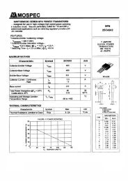
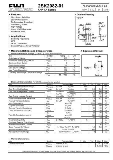
<strong>2SK2082</strong>-<strong>01</strong>N-channel MOS-FETFAP-IIA Series 900V 1,4Ω 9A 150W>Features- High Speed Switching- Low On-Resistance- No Secondary Breakdown- Low Driving Power- High Voltage- VGS = ± 30V Guarantee- Avalanche Proof> Outline Drawing>Applications- Switching Regulators- UPS- DC-DC converters- General Purpose Power Amplifier>Maximum Ratings and Characteristics- Absolute Maximum Ratings (TC=25°C), unless otherwise specifiedItem Symbol Rating UnitDrain-Source-Voltage V DS 900 VDrain-Gate-Voltage (R GS =20KΩ) V DGR 900 VContinous Drain Current I D 9 APulsed Drain Current I D(puls) 36 AGate-Source-Voltage V GS ±30 VMax. Power Dissipation P D 150 WOperating and Storage Temperature Range T ch 150 °CT stg -55 ~ +150 °C> Equivalent Circuit- Electrical Characteristics (T C =25°C), unless otherwise specifiedItem Symbol Test conditions Min. Typ. Max. UnitDrain-Source Breakdown-Voltage V (BR)DSS I D =1mA V GS =0V 900 VGate Threshhold Voltage V GS(th) I D =1mA V DS= V GS 2,5 3,0 3,5 VZero Gate Voltage Drain Current I DSS V DS =900V T ch =25°C 10 500 µAV GS =0V T ch =125°C 0,2 1,0 mAGate Source Leakage Current I GSS V GS =±30V V DS =0V 10 100 nADrain Source On-State Resistance R DS(on) I D =4,5A V GS =10V 1,1 1,4 ΩForward Transconductance g fs I D =4,5A V DS =25V 5 10 SInput Capacitance C iss V DS =25V 2200 3300 pFOutput Capacitance C oss V GS =0V 210 320 pFReverse Transfer Capacitance C rss f=1MHz 65 100 pFTurn-On-Time t on (t on =t d(on) +t r ) t d(on) V CC =600V 25 40 nst r I D =9A 60 90 nsTurn-Off-Time t off (t on =t d(off) +t f ) t d(off) V GS =10V 140 210 nst f R GS =10 Ω 70 110 nsAvalanche Capability I AV L = 100µH T ch =25°C 9 AContinous Reverse Drain Current I DR 9 APulsed Reverse Drain Current I DRM 36 ADiode Forward On-Voltage V SD I F =2xI DR V GS =0V T ch =25°C 1,2 1,8 VReverse Recovery Time t rr I F =I DR V GS =0V 450 nsReverse Recovery Charge Q rr -dI F /dt=100A/µs T ch =25°C 4 µC- Thermal CharacteristicsItem Symbol Test conditions Min. Typ. Max. UnitThermal Resistance R th(ch-a) channel to air 35 °C/WR th(ch-c) channel to case 0,833 °C/WCollmer Semiconductor, Inc. - P.O. Box 702708 - Dallas, TX - 75370 - 972-233-1589 - FAX 972-233-0481 - http://www.collmer.com
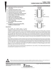
<strong>2SK2082</strong>-<strong>01</strong>N-channel MOS-FET900V 1,4Ω 9A 150W FAP-IIA Series> CharacteristicsTypical Output Characteristics Drain-Source-On-State Resistance vs. T ch Typical Transfer Characteristics↑ 1 ↑ 2 ↑ 3ID [A]RDS(ON) [Ω]ID [A]VDS [V] → Tch [°C] → VGS [V] →Typical Drain-Source-On-State-Resistance vs. I D Typical Forward Transconductance vs. I D Gate Threshold Voltage vs. T ch↑ 4 4 ↑ 5 ↑ 6RDS(ON) [Ω]gfs [S]VGS(th) [V]ID [A] → ID [A] → Tch [°C] →Typical Capacitance vs. V DS Typical Input Charge Forward Characteristics of Reverse Diode↑ 7 ↑ 8 ↑ ↑ 9C [nF]VDS [V]VGS [V]IF [A]VDS [V] → Qg [nC] → VSD [V] →Allowable Power Dissipation vs. T CSafe operation area↑↑ 10 ↑ 12 11PD [W]ID [A]Zth(ch-c) [K/W]Transient Thermal impedanceTc [°C] → VDS [V] → t [s] →This specification is subject to change without notice!