
Create successful ePaper yourself
Turn your PDF publications into a flip-book with our unique Google optimized e-Paper software.
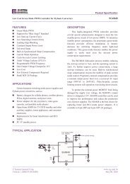
November 2,1999AN4003PC POWER SUPPLY DESIGN WITH <strong>KA3511</strong>Sang-Tae Im1. GENERAL DESCRIPTIONThe <strong>KA3511</strong> is a fixed-frequency improved-performance pulse-width modulation control circuit withcomplete housekeeping circuitry for use in the secondary side of SMPS (Switched mode powersupply). It contains various functions, which are precision voltage reference, over voltage protection,under voltage protection, remote on/off control, power good signal generator and etc.OVP (Over voltage protection) sectionIt has OVP functions for +3.3V,+5V,+12V and PT outputs. The circuit is made up of a comparatorwith four detecting inputs and without hysteresis voltage. Especially, PT (Pin16) is prepared for anextra OVP input or another protection signal.UVP (Under voltage protection) sectionIt also has UVP functions for +3.3V, +5V, +12V outputs. The block is made up of a comparator withthree detecting inputs and without hysteresis voltage.Remote on/off sectionRemote on/off section is used to control SMPS externally. If a high signal is supplied to the remoteon/off input, PWM signal becomes a high state and all secondary outputs are grounded. Theremote on/off signal is transferred with some on-delay and off-delay time of 8ms, 24ms respectively.Precision reference sectionThe reference voltage trimmed to ±2% (4.9V
ORDERING INFORMATIONDevice Package Operating Temperature<strong>KA3511</strong> 22 DIP -25°C ~ 85°C22-DIP-400FEATURES• Complete PWM control and house keeping circuitry• Few external components• Precision voltage reference trimmed to 2%• Dual output for push-pull operation• Each output TR for 200mA sink current• Variable duty cycle by dead time control• Soft start capability by using dead time control• Double pulse suppression logic• Over voltage protection for 3.3V / 5V / 12V• Under voltage protection for 3.3V / 5V / 12V• One more external input for various protection (PT)• Remote on/off control function (PS-ON)• Latch function controlled by remote and protection input• Power good signal generator with hysteresis• 22-Pin dual in-line package2. BLOCK DIAGRAMV5V12R TC TCOMP782OSCILLATORPWMCONTROLDCKQQ222021C1C2EE/A(-)E/A(+)DEAD TIMECONTROLVREFV CC341912 VREF15V1.25VStart UpINTERNALBIAS0.1VCOMP1DEAD TIMECONTROLLERVREFIchag5VQRSPGGENERATORDELAYCONTROLLERVREFOVPCOMP1.25VREMOTE ON/OFF1.4V5T REM6REM(PS-ON)1116151413PGPTV12V5V3.3DET9COMP2COMP31.8V 0.6V1.8V 0.6V1.25VUVPCOMP1.25VT PG102.2uFT UVP2.2uF17 18GNDRev C, November 19992
3. PIN DESCRIPTIONC1EC2DTCGNDTUVPPTV12V5V3.3Vref#22#12<strong>KA3511</strong>#1 #11V CCCOMPE/A(-) EA(+) TREM REM RT CT DET TPG PGPinNo. Name I/O FunctionPinNo. Name I/O Function1 V CC I Supply voltage 12 Vref O Precision reference VTG2 COMP O E/A output 13 V3.3 I OVP, UVP input for 3.3V3 E/A(-) I E/A (-) input 14 V5 I OVP, UVP input for 5V4 E/A(+) I E/A (+) input 15 V12 I OVP, UVP input for 12V5 TREM – Remote on/off delay 16 PT I Extra protection input6 REM I Remote on/off input 17 T UVP – UVP delay7 RT – Oscillation freq. setting R 18 GND – Signal ground8 CT – Oscillation freq. setting C 19 DTC I Deadtime control input9 DET I Detect input 20 C2 O Output 210 T PG – PG delay 21 E – Power ground11 PG O Power good signal output 22 C1 O Output 13Rev C, November 1999
PinNo. Name Function1 V CC Supply voltage. Operating range is 14V~30V. V CC =20V, Ta=25°C at test.2 COMP Error amplifier output. It is connected to non-inverting input of pulse widthmodulator comparator.3 E/A(-) Error amplifier inverting input. Its reference voltage is always 1.25V.4 E/A(+) Error amplifier non-inverting input feedback voltage.This pin may be used tosense power supply output voltage.5 TREM Remote on/off delay. Ton/Toff=8ms/24ms (Typ.) with C=0.1µF. Its high/lowthreshold voltage is 1.8V/0.6V.6 REM Remote on/off input. It is TTL operation and its threshold voltage is 1.4V. Voltageat this pin can reach normal 4.6V, with absolutely maximum voltage, 5.25V. IfREM = “Low”, PWM = “Low”. That means the main SMPS is operational. WhenREM = “High”, then PWM = “High” and the main SMPS is turned-off.7 RT Oscillation frequency setting R. (Test Condition R T =10kΩ)8 CT Oscillation frequency setting C. (Test Condition C T =0.01µF)9 DET Under-voltage detect pin. Its threshold voltage is 1.25V Typ.10 T PG PG delay. Td=250ms (Typ) with C PG =2.2µF. The high/low threshold voltage are1.8V/0.6V and the voltage of Pin10 is clamped at 2.9V for noise margin.11 PG Power good output signal. PG = “High” means that the power is “Good” foroperation and PG = “Low” means “Power fail”.12 Vref Precision voltage reference trimmed to 2%. (Typical Value = 5.03V)13 V3.3 Over voltage protection for output 3.3V. (Typical Value = 4.1V)14 V5 Over voltage protection for output 5V. (Typical Value = 6.2V)15 V12 Over voltage protection for output 12V. (Typical Value = 14.2V)16 PT This is prepared for an extra OVP input or another protection signal. (TypicalValue = 1.25V)17 T UVP Timing pin for under voltage protection blank-out time. Its threshold voltage is1.8V and clamped at 2.9V after full charging. Target of delay time is 250ms andit is realized through external (C=2.2µF).18 GND Signal ground.19 DTC Deadtime control input. The dead-time control comparator has an effective120mV input offset which limits the minimum output dead time. Dead time maybe imposed on the output by setting the dead time control input to a fixedvoltage, ranging between 0V to 3.3V.20 C2 Output drive pin for push-pull operation.21 E Power ground.22 C1 Output drive pin for push-pull operation.4Rev C, November 1999
4. ABSOLUTE MAXIMUM RATINGSCharacteristic Symbol Value UnitSupply voltage V CC 40 VCollector output voltage V C1 , V C2 40 VCollector output current I C1 , I C2 200 mAPower dissipation P D 1 WOperating temperature T OPR -25 to 85 °CStorage temperature T STG -65 to 150 °CTEMPERATURE CHARACTERISTICSValueCharacteristicSymbol Min. Typ. Max. UnitTemperature coefficient of Vref (-25 °C
5. ELECTRICAL CHARACTERISTICS (V CC =20V, T A =25°C)ValueCharacteristic Symbol Test Condition Min. Typ. Max. UnitREFERENCE SECTIONReference output voltage Vref Iref=1mA 4.9 5 5.1 VLine regulation ∆Vref. LINE 14V
5. ELECTRICAL CHARACTERISTICS (continued)ValueCharacteristic Symbol Test Condition Min. Typ. Max. UnitOver voltage protection for 5V V OVP2 – 5.8 6.2 6.6 VOver voltage protection for 12V V OVP3 – 13.5 14.2 15.0 VInput threshold voltage for PT V PT – 1.20 1.25 1.30Under voltage protection for 3.3V V UVP1 – 2.1 2.3 2.5 VUnder voltage protection for 5V V UVP2 – 3.7 4.0 4.3 VUnder voltage protection for 12V V UVP3 – 9.2 10 10.8 VCharging current for UVP delay I CHG.UVP C=2.2µF, V TH =1.8V -10 -15 -23 uAUVP Delay Time T D.UVP C=2.2µF 100 260 500 msREMOTE ON/OFF SECTIONREM on input voltage V REMH I REM = -200µA 2.0 – – VREM off input voltage V REML – – – 0.8 VREM off input bias voltage I REML V REM =0.4V – – -1.6 mAREM on open voltage V REM(OPEN) – 2.0 – 5.25 VREM on delay time Ton C=0.1µF 4 8 14 msREM off delay time Toff C=0.1µF 16 24 34 msREMOTE ON/OFF SECTION (2)Detecting input voltage V IN(DET) – 1.20 1.25 1.30 VDetecting V5 voltage V 5(DET) – 4.1 4.3 4.5 VHysteresis voltage 1 HY1 COMP1, 2 10 40 80 mVHysteresis voltage 2 HY2 COMP3 0.6 1.2 – VPG output load resistor R PG – 0.5 1 2 kΩCharging current for PG delay I CHG.PG C=2.2µF, V TH =1.8V -10 -15 -23 uAPG delay time T D.PG C=2.2µF 100 260 500 msPG output saturation voltage V SAT(PG) I PG =10mA – 0.4 0.2 VTOTAL DEVICEStandby supply current I CC – – 10 20 mANotes:1. These Parameters, although guaranteed over their recommended operating conditions are not 100%tested in production.2. REM on delay time (Pin6 REM: “L” → “H”),REM off delay time (Pin6 REM: “H” → “L”)7Rev C, November 1999
6. BLOCK DESCRIPTION & APPLICATION INFORMATIONS6.1 OSCILLATOR BLOCKVrefV CC12 112R TC T12Figure 1. Oscillator R T , C TThe <strong>KA3511</strong> is a fixed-frequency pulse width modulation control circuit. An internal-linear sawtoothoscillator is frequency-programmable by two external components, R T and C T . The oscillator frequencyis determined by1.1fosc = --------------------×R TC T300K100KVCC=15VI O - OSCILLATOR FREQUENCY10K1K1001.0µF0.1µFCT=0.01µF0.001µF301K2K 5K 10K 20K 50K 100K 200K 500K 1MR T . TIMING RESISTANCE( Ω)6.2 PWM CONTROL BLOCKFigure 2. Oscillator Frequency vs. Timing ResistanceOutput pulse width modulation is accomplished by comparison of the positive sawtooth waveformacross capacitor C T to either of two control signals. The NOR gates, which drive output transistorsQ1 and Q2, are enabled only when the flip-flop clock-input line is in its low state. This happens onlyduring that portion of time when the sawtooth voltage is greater than the control signals. Therefore,an increase in control-signal amplitude causes a corresponding linear decrease of output pulsewidth. (Refer to the timing diagram shown in Figure 4)8Rev C, November 1999
R TC T78OSCILLATORDQOutputDriveQ12COMPPWMCONTROLCKQQ2431.25V0.12VDEAD TIMECONTROLLERFigure 3. PWM Control BlockThe control signals are external inputs that can be fed into the dead-time control, the error amplifierinputs, or the feedback input. The dead-time control comparator has an effective 120mV input offsetwhich limits the minimum output dead time. Dead time may be imposed on the output by settingthe dead time control input to a fixed voltage, ranging between 0V to 3.3V.The pulse width modulator comparator provides a means for the error amplifier to adjust the outputpulse width from the maximum percent on-time, established by the dead time control input, downto zero, as the voltage at the feedback pin varies from 0.5V to 3.5V. The error amplifier may beused to sense power-supply output voltage, and its output is connect to noninverting input of thepulse width modulator comparator. With this configuration, the amplifier that demands minimumoutput on time, dominates control of the loop.When capacitor C T is discharged, a positive pulse is generated on the output of the dead timecomparator, which clocks the pulse-steering flip-flop and inhibits the output transistors, Q1 and Q2.The pulse-steering flip-flop directs the modulated pulses to each of the two output transistorsalways for push-pull operation. The output frequency is equal to half that of the oscillator.The <strong>KA3511</strong> has an internal 5.0V reference capable of sourcing up to 10mA of load current forexternal bias circuits. The reference has an internal accuracy of ±2% with typical thermal drift ofless than 50mV over an operating temperature range of -25°C to 85°C9Rev C, November 1999
FeedbackCtDead-timecontrolCkQQOutput Q1Output Q2Figure 4. Operating Waveform6.3 DEADTIME CONTROL for SOFT-START123mAVrefR147k+C122uFDTC19RemoteON/OFFR21kFigure 5. Soft-Start CircuitDeadtime control for soft-start makes a power supply output rising time (Typ. 15ms) to reduce outputringing voltage for 3.3V, 5V, and 12V. If output rising time is too fast, output ringing voltagereaches OVP level.You can make a soft start function by add external components R1, R2 and C1 (refer to figure 5).At first the main power is turned-on, the deadtime control voltage keeps high state ( · = · 3V), andthen go to the low voltage( · = · 105mV) that devided by R1, R2.V DTC LOWR2= --------------------- × Vref(5V) = 104.9mVR1 + R210Rev C, November 1999
So Output Duty Ratio will change from the minimum duty ratio to the maximum duty ratio.Also, if the remote voltage is high, the deadtime control voltage will keep 3V (=3mA xR2 (1kΩ)) bythe internal 3mA current source for soft start. Therefore, when the remote voltage is low, the deadtimecontrol voltage will be changed from 3V to almost ground potential. And its soft start timedependent on external capacitor C1.6.4 OUTPUT VOLTAGE REGULATION+5V +12VR111kΩR233kΩR51kΩCOMP2E/A(+)VrefR32kΩR41kΩC110343E/A(-)1.25VErr-AmpPWM ControlComparatorFigure 6. Output Regulation Circuit+5V/+12V output voltages are determined by resistor ratio of R1,R2,R3 and R4. The resistor valuecan be changed by set condition and requirements.R5, C1 are the compensation circuit for stability.If output voltage (+5V or +12V) is increase, duty ratio of main power switch will be reduced byPWM control comparator signal and error amplifier output. Therefore the output voltage will bereduced.On the contrary, if output voltage (+5V or +12V) is reduce, duty ratio of main power switch will beincreased by PWM control comparator signal and error amplifier output. Therefore the output voltagewill be increased. So the output voltage of power supply will be regulated.11Rev C, November 1999
6.5 OVP BLOCKVO3.3V 5V 12V13 14 15DR101PT16R102AR1BR2R3CR4R5R61.25VVref=5VOVP COMPSET ofR/S LatchR102, R102: External ComponentsOVP function is simply realized by connecting Pin13, Pin14, Pin15 to each secondary output. R1,2, 3, 4, 5, 6 are internal resistors of the IC. Each OVP level is determined by resistor ratio and thetypical values are 4.1V/6.2V/14.2V.OVP Detecting voltage for +3.3VV OVP 1( +3.3V)R 1+ R 2 R 1+ R 2= -------------------- × V A= -------------------- × Vref = 4.1VR 2R 2OVP Detecting voltage for +5VV OVP 2( +5V)OVP Detecting voltage for +12VV OVP 3( +12V)Especially, pin16 (PT) is prepared for extra OVP input or another protection signal. That is, if youwant over voltage protection of extra output voltage, then you can make a function with two externalresistors.OVP Detecting voltage for PTR 3+ R 4 R 3+ R 4= -------------------- × V B= -------------------- × Vref = 6.2VR 4In the case of OVP, system designer should know a fact that the main power can be dropped aftera little time because of system delay, even if PWM is triggered by OVP.So when the OVP level is tested with a set, you should check the secondary outputs (+3.3V/+5V/+12V) and PG (Pin11) simultaneously. you can know the each OVP level as checking each outputvoltage in just time that PG (Pin11) is triggered from high to low.R 4R 5+ R 6R 5+ R 6= -------------------- × V C= -------------------- × Vref = 14.2VR 6R 6R 101+ R 102 R 101+ R 102V PT= ------------------------------ × V D= ------------------------------ × VrefR 102R 10212Rev C, November 1999
6.6 UVP BLOCK3.3V 5V 12V13 14 15R1R3R5Vref=5VABR2CR2UVP COMPSET ofR/S LatchR6 1.25VThe <strong>KA3511</strong> has UVP functions for +3.3V, +5V, +12V Outputs. The block is made up of three inputcomparators. Each UVP level is determined by resistor ratio and the typical values are 2.3V/4V/10V.UVP Detecting voltage for +3.3VV UVP 1( +3.3V)R 1+ R 2 R 1+ R 2= -------------------- × V A= -------------------- × Vref = 2.3VR 2R 2UVP Detecting voltage for +5VV UVP 2( +5V)UVP Detecting voltage for +12VV UVP 3( +12V)R 1+ R 2 R 1+ R 2= -------------------- × V A= -------------------- × Vref = 4VR 2R 2R 1+ R 2 R 1+ R 2= -------------------- × V A= -------------------- × Vref = 10VR 2R 213Rev C, November 1999
6.7 REMOTE ON/OFF & DELAY BLOCKVrefTonToff125VREMPWMRpullIonTrem5BCCOMP6Ion/Ioff+ 2.2VTrem0.1uFCOMP0.6V 1.8VPGBlockQ1Q2REM6Remote On/OffFigure 9. Remote ON/OFF Delay BlockRemote ON/OFF section is controlled by a microprocessor. If a high signal is supplied to theremote ON/OFF input (Pin6), the output of COMP6 becomes high status. The output signal istransferred to ON/OFF delay block and PG block.If no signal is supplied to Pin6, Pin6 maintains high status (=5V) for Rpull.When Remote ON/OFF is high, it produces PWM (Pin6) “High” signal after ON delay time (about8ms) for stabilizing system.Then, all outputs (+3.3V, +5V, +12V) are grounded.When Remote ON/OFF is changed to “Low”, it produces PWM “Low” signal after OFF delay time(about 24ms) for stabilizing the system.If REM is low, then PWM is low. That means the main SMPS is operational. When REM is high,PWM is high and the main SMPS is turned-off.ON/OFF delay Time can be calculated by following equation.Ctrem × ∆Von 0.1µF 2VTon = K 1× -------------------------------------- ≈ 0.95 × -----------------------------× = 8.2msecIon23µACtrem × ∆Voff 0.1µF 2.1VToff = K 2× --------------------------------------- ≈ 0.8 × ----------------------------------× = 24msecIoff8µA(K1, K2: Constant value gotten by test)In above equation, typical capacitor value is 0.1uF. If the capacitor is changed to larger value, itcan cause malfunction in case of AC power on at remote High. Because PWM maintains low statusand main power turns on for on delay time. So you should use 0.1uF or smaller capacitor.14Rev C, November 1999
6.8 R/S FLIP FLOP (LATCH) BLOCKR-S F/F (LATCH)PG BLOCKREMOTEON/OFFR-S FFOVPUVPSNORQON/OFFDELAYStart-upDelayedREMOTERNORQPGgeneratorFigure 10. R-S F/F Block DiagramOVP+ SET RESET Qn+1 Qn+1Low Low Low Qn QnLow Low High High HighHigh High Low High LowHigh Low High Low HighThere is a R-S F/F (Latch) circuit for shutdown operation in the <strong>KA3511</strong>. R-S F/F (Latch) is controlledby OVP, UVP, and some delayed remote ON/OFF signal.If any output of OVP or UVP is High, SET signal of R-S F/F is high status and it produces PWM“High” and main power is turned off. When remote signal is high, its delayed output signal is suppliedto RESET port of R-S F/F and it produces SET low. So output Q is low status. At this time,PWM maintains high status by delayed remote high signal.After main power is turned-off by OVP/UVP and initialized by remote, if remote signal is changed tolow, main power becomes operational.When you test <strong>KA3511</strong>, Remote ON/OFF signal should be toggled once for initializing.15Rev C, November 1999
6.9 POWER GOOD SIGNAL GENERATORVref +5V1214V CCR13IchgR151kR1160kVrefCOMP1PG COMPQ311PGCOMP3DET9VrefQ20.6V 1.8VR124.7kR14COMP2Remote1.25VON/OFF10TPG+CPG2.2uFFigure 11. PG Signal Generator BlockPower good signal generator curcuits generate “ON & OFF” signal depending on the status of outputvoltage to prevent the malfunctions of following systems like microprocessor and etc. fromunstable outputs at power on & off. At power on, it produces PG “High” signal after some delay(about 250ms) for stabilizing outputs.At power off, it produces PG “Low” signal without delay by sensing the status of power source forprotecting following systems. V CC detection point can be calculated by following equation. recommendedvalues of R11, R12 are external components.V DET= 1.25V × ⎛1 + R11 ----------⎞⎝ R12⎠= 17.2VCOMP3 creates PG “Low” without delay when +5V output falls to less than 4.3V to prevent somemalfunction at transient status, thus it improves system stability.When remote On/Off signal is high, it generates PG “Low” signal without delay. It means that PGbecomes “Low” before main power is grounded.PG delay time (Td) is determined by capacitor value, threshold voltage of COMP3 and the chargingcurrent and its equation is as following.∆V PG × Vth 2.2µF × 2VTd = ----------- ≈ ------------------------ = ----------------------------- ≈ 250msIchg Ichg 18µA16Rev C, November 1999
Considering the lightning surge and noise, there are two types of protections. One is a few secondsdelay between TPG and PG for safe operation and another is some noise margin of Pin10.Noise_Margin_of_T PG = V10(max) – Vth(L) = 2.9V – 0.6V = 2.3V7. ABOUT TEST METHODYou can verify the <strong>KA3511</strong> with a SMPS set. But you should pay attention to the device damageproblem by increasing V CC . You should remove the sub-board after +5Vsb drops to 0V and V CC of<strong>KA3511</strong> is grounded and then fan stops under the Remote Low.– OVP function of +3.3V/+5V/+12VYou can test OVP for +3.3V/+5V/+12V by shorting Pin16 and Pin17 to GND.– UVP function of +3.3V/+5V/+12VYou can simply test UVP for +3.3V/+5V/+12V by shorting Pin16 to GND.– OVP input threshold voltage for PTThe test condition is remote “Low” and you increase the supply voltage of pin16 using a DCpower supply. When the voltage is over 1.2 x V, main power supply will shutdown. So, you canmeasure the shutdown point of main power supply, and that will be a OVP input threshold voltagefor PT.– Remote On/Off delay timeYou can measure the time difference of remote On/Off and the main power supply output astoggling the remote On/Off.– PG delay timeIn AC power-on time, secondary outputs are turned on and then after some delay time PG outputis triggered from low to high. You can measure the time difference of +5V and PG in turn-ontime.17Rev C, November 1999
8. HOUSE KEEPING CIRCUIT2kΩ(1W)2kΩ(1W)StandbySupplyV CC =20V1VCCC12212V5V15kΩ2COMPE2111kΩ33kΩ0.01uF3E/A(-)C2201.8kΩ0.1uF1kΩ+Micom4567E/A(+)T REMREMRT<strong>KA3511</strong>DTCGNDT UVPPT191817162.2uF+12kΩ0.01uF+8CTV121512V9DETV5145V10T PGV3.3133V2.2uF+PG11PGVref121uF+Using the <strong>KA3511</strong> requires few external components to accomplish a complete housekeeping circuitsfor SMPS.18Rev C, November 1999
9. TYPICAL CHARACTERISTICSV CC -I CCBandgap Reference VoltageTemperature Characteristic0.0140.0125.0100.0105.008I CC [A]0.0080.006Vref [V]5.0060.0045.0040.0020.0000 10 20 30 40Supply Voltage [V]5.002-40 -20 0 20 40 60 80 100 120 140TEMP [°C]PIN19(Dead Time Control Voltage)-Duty Cycle OVP for 3.3V505404Duty Ratio [%]30201031.1%21.8%12.8%VPG [V]321000.0 0.5 1.0 1.5 2.0 2.5 2.73 3.0Deadtime Control Voltage [V]3.6 3.8 4.0 4.2 4.4 4.6V3.3 [V]OVP for 5VOVP for 12V76554VPG [V]432VPG [V]3211005.0 5.5 6.0 6.5 7.0V5 [V]14.0 14.2 14.4 14.6 14.8 15.0V12 [V]Rev C, November 199919
OVP for PT UVP for 3.3V5544VPG [V]32VPG [V]3211001.15 1.20 1.25 1.30 1.3521 22 23 24 25Vpt [V]Pin 13 (V3.3) Voltage [V]UVP for 5VUVP for 12V5544VPG [V]32VPG [V]3211003.6 3.8 4.0 4.2 4.4 4.6 4.8 5.0Pin 14 (V5) Voltage [V]9.0 9.5 10.0 10.5 11.0Pin 15 (V12) Voltage [V]Remote ON Charging CurrentREM ON/OFF Vth-0.0000165-0.0000184Irem [A]-0.000020-0.000022VPG [V]321-0.00002400 50 100 150 200 2500 1 2 3 4 5Vrem [V]Rev C, November 199920
Remote ON Open VoltageDetecting V CC Voltage (DET)5544Vrem [V]32VPG [V]32100 1 2 3 4 5101.0 1.1 1.2 1.3 1.4 1.5Pin 9 (DET) Voltage [V]Detecting V5 VoltageCharging Current for PG-0.00000554-0.000010VPG [V]32IPG [V]-0.0000151-0.00002004.0 4.2 4.4 4.6 4.8 5.0Pin 14 (5V) Voltage [V]0 20 40 60 80 100 120 140 160Short Circuit Current Hysteresis Voltage 2-0.03254Iref [A]-0.033-0.034VPG [V]321-0.03500 100 200 300 4000.0 0.5 1.0 1.5 2.0 2.5Pin 10 (T PG) Voltage [V]Rev C, November 199921
Error Amp Sink CurrentReference Voltage0.0025Isink & Isource [A]0.00-0.002-0.004-0.006Vref [V]4321-0.0080 20 40 60 80 100 120 14000 10 20 30 40Supply Voltage [V]Rev C, November 199922
10. PACKAGE DIMENSION9.14 ±0.200.360 ±0.00822-DIP-40011.05( )0.0412227.901.098 MAX27.49 ±0.201.082 ±0.0081.52 ±0.100.060 ±0.0040.46 ±0.100.018 ±0.00411 122.540.10010.160.4003.81 ±0.200.150 ±0.0080.510.020MIN5.080.200MAX3.40 ±0.300.134 ±0.0120~15°0.25 +0.10–0.050.010 +0.004–0.00223Rev C, November 1999
11. EXPERIMENTAL RESULTCH1 : PS-ONCH2 : +5Vdc OutputCH3 : PG SignalFigure 12. Rising Time of +5Vdc Output VoltageCH1 : PS-ONCH2 : +5Vdc OutputCH3 : PG SignalFigure 13. PG Signal Delay Time24Rev C, November 1999
CH1 : PS-ONCH2 : +5Vdc OutputCH3 : PG SignalFigure 14. Power Down WarningCH1 : +3.3Vdc OutputCH2 : +5Vdc OutputCH3 : +12Vdc OutputFigure 15. No Load ProtectionRev C, November 199925
CH1 : VccCH2 : +5Vdc OutputCH3 : PG SignalFigure 16. Vcc, +5Vdc Output vs. PG Signal (High)CH1 : VccCH2 : +5Vdc OutputCH3 : PG SignalFigure 16. Vcc, +5Vdc Output vs. PG Signal (Low)26Rev C, November 1999
12. APPLICATION CIRCUIT47K70KVCCR6R5103IC11VccC122C12COMPE 21POWER ON15K34E/A(-)E/A(+)C220DTC 19C2R41.2KOUT REF+0.1uF567TREMREMRTGND 18TUVP17PT162.2uF+R356K+C622uF10389CTDETV12V5151412V OUT5V OUTPG+2.2uF1011TPGPGV3.3Vref13123.3V OUTAR3511XD19100KC16+VR1D9CTReference1. Power Electronics by Marvin J. Fisher2. Principles Of Power Electronics by KassakianAUTHOR:Sang-Tae Im: P-IC Application TeamTel. 82-32-680-1275Fax. 82-32-680-1317E-mail. sangtae.im@Fairchildsemi.co.krRev C, November 199927
TRADEMARKSThe following are registered and unregistered trademarks Fairchild Semiconductor owns or is authorized to use and isnot intended to be an exhaustive list of all such trademarks.DISCLAIMERACExCoolFETCROSSVOLTE 2 CMOS TMFACTFACT Quiet SeriesFAST ®FASTrGTOHiSeCISOPLANARMICROWIREPOPPowerTrench®QFETQSQuiet SeriesSuperSOT-3SuperSOT-6SuperSOT-8TinyLogicUHCVCXFAIRCHILD SEMICONDUCTOR RESERVES THE RIGHT TO MAKE CHANGES WITHOUT FURTHERNOTICE TO ANY PRODUCTS HEREIN TO IMPROVE RELIABILITY, FUNCTION OR DESIGN. FAIRCHILDDOES NOT ASSUME ANY LIABILITY ARISING OUT OF THE APPLICATION OR USE OF ANY PRODUCTOR CIRCUIT DESCRIBED HEREIN; NEITHER DOES IT CONVEY ANY LICENSE UNDER ITS PATENTRIGHTS, NOR THE RIGHTS OF OTHERS.LIFE SUPPORT POLICYFAIRCHILD’S PRODUCTS ARE NOT AUTHORIZED FOR USE AS CRITICAL COMPONENTS IN LIFE SUPPORTDEVICES OR SYSTEMS WITHOUT THE EXPRESS WRITTEN APPROVAL OF FAIRCHILD SEMICONDUCTOR CORPORATION.As used herein:1. Life support devices or systems are devices orsystems which, (a) are intended for surgical implant intothe body, or (b) support or sustain life, or (c) whosefailure to perform when properly used in accordancewith inst<strong>ru</strong>ctions for use provided in the labeling, can bereasonably expected to result in significant injury to theuser.PRODUCT STATUS DEFINITIONSDefinition of Terms2. A critical component is any component of a lifesupport device or system whose failure to perform canbe reasonably expected to cause the failure of the lifesupport device or system, or to affect its safety oreffectiveness.Datasheet Identification Product Status DefinitionAdvance InformationPreliminaryNo Identification NeededFormative orIn DesignFirst ProductionFull ProductionThis datasheet contains the design specifications forproduct development. Specifications may change inany manner without notice.This datasheet contains preliminary data, andsupplementary data will be published at a later date.Fairchild Semiconductor reserves the right to makechanges at any time without notice in order to improvedesign.This datasheet contains final specifications. FairchildSemiconductor reserves the right to make changes atany time without notice in order to improve design.ObsoleteNot In ProductionThis datasheet contains specifications on a productthat has been discontinued by Fairchild semiconductor.The datasheet is printed for reference information only.