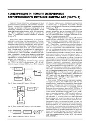
electro-tech.narod.ru, TL594
electro-tech.narod.ru, TL594
electro-tech.narod.ru, TL594
- No tags were found...

Create successful ePaper yourself
Turn your PDF publications into a flip-book with our unique Google optimized e-Paper software.
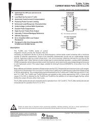
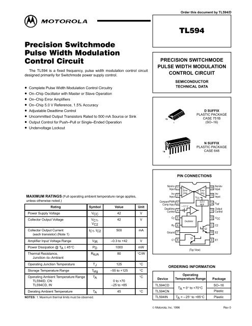
Order this document by <strong>TL594</strong>/D The <strong>TL594</strong> is a fixed frequency, pulse width modulation control circuitdesigned primarily for Switchmode power supply control.• Complete Pulse Width Modulation Control Circuitry• On–Chip Oscillator with Master or Slave Operation• On–Chip Error Amplifiers• On–Chip 5.0 V Reference, 1.5% Accuracy• Adjustable Deadtime Control• Uncommitted Output Transistors Rated to 500 mA Source or Sink• Output Control for Push–Pull or Single–Ended Operation• Undervoltage LockoutPRECISION SWITCHMODEPULSE WIDTH MODULATIONCONTROL CIRCUITSEMICONDUCTORTECHNICAL DATAD SUFFIXPLASTIC PACKAGECASE 751B(SO–16)N SUFFIXPLASTIC PACKAGECASE 648PIN CONNECTIONSMAXIMUM RATINGS (Full operating ambient temperature range applies,unless otherwise noted.)Rating Symbol Value UnitPower Supply Voltage VCC 42 VCollector Output VoltageCollector Output Current(each transistor) (Note 1)VC1,42 VVC2IC1, IC2 500 mAAmplifier Input Voltage Range VIR –0.3 to +42 VPower Dissipation @ TA ≤ 45°C PD 1000 mWThermal Resistance,Junction–to–AmbientRθJA 80 °C/WOperating Junction Temperature TJ 125 °CStorage Temperature Range Tstg –55 to +125 °COperating Ambient Temperature Range<strong>TL594</strong>ID, CN<strong>TL594</strong>CD, INTA0 to +70–25 to +85Derating Ambient Temperature TA 45 °CNOTES: 1. Maximum thermal limits must be observed.°CDevice<strong>TL594</strong>CD<strong>TL594</strong>CNNoninvInputInvInputR TGroundC112Compen/PWNComp Input3DeadtimeControl4C T 5<strong>TL594</strong>IN+Error1Amp–V CC5.0 VREF(Top View)2 Error+Amp–ORDERING INFORMATIONOperatingTemperature RangeTA = 0° to +70°CTA = – 25° to +85°C1615NoninvInputInvInput14 V ref≈ 0.1 V13OutputControl12 V CCOscillator611 C2Q278Q1109E2E1PackageSO–16PlasticPlasticMOTOROLA ANALOG IC DEVICE DATA© Motorola, Inc. 1996 Rev 01
<strong>TL594</strong>RECOMMENDED OPERATING CONDITIONSCharacteristics Symbol Min Typ Max UnitPower Supply Voltage VCC 7.0 15 40 VCollector Output Voltage VC1, VC2 – 30 40 VCollector Output Current (Each transistor) IC1, IC2 – – 200 mAAmplified Input Voltage Vin 0.3 – VCC – 2.0 VCurrent Into Feedback Terminal lfb – – 0.3 mAReference Output Current lref – – 10 mATiming Resistor RT 1.8 30 500 kΩTiming Capacitor CT 0.0047 0.001 10 µFOscillator Frequency fosc 1.0 40 200 kHzPWM Input Voltage (Pins 3, 4, 13) – 0.3 – 5.3 VELECTRICAL CHARACTERISTICS (VCC = 15 V, CT = 0.01 µF, RT = 12 kΩ, unless otherwise noted.)For typical values TA = 25°C, for min/max values TA is the operating ambient temperature range that applies, unless otherwise noted.Characteristics Symbol Min Typ Max UnitREFERENCE SECTIONReference VoltageVrefV(IO = 1.0 mA, TA = 25°C)4.925 5.0 5.075(IO = 1.0 mA)4.9–5.1Line Regulation (VCC = 7.0 V to 40 V) Regline – 2.0 25 mVLoad Regulation (IO = 1.0 mA to 10 mA) Regload – 2.0 15 mVShort Circuit Output Current (Vref = 0 V) ISC 15 40 75 mAOUTPUT SECTIONCollector Off–State Current (VCC = 40 V, VCE = 40 V) IC(off) – 2.0 100 µAEmitter Off–State Current (VCC = 40 V, VC = 40 V, VE = 0 V) IE(off) – – –100 µACollector–Emitter Saturation Voltage (Note 2)VCommon–Emitter (VE = 0 V, IC = 200 mA)VSAT(C) –1.1 1.3Emitter–Follower (VC = 15 V, IE = –200 mA)VSAT(E) –1.5 2.5Output Control Pin CurrentLow State (VOC ≤ 0.4 V)High State (VOC = Vref)Output Voltage Rise TimeCommon–Emitter (See Figure 13)Emitter–Follower (See Figure 14)Output Voltage Fall TimeCommon–Emitter (See Figure 13)Emitter–Follower (See Figure 14)IOCLIOCHtrERROR AMPLIFIER SECTIONInput Offset Voltage (VO (Pin 3) = 2.5 V) VIO – 2.0 10 mVInput Offset Current (VO (Pin 3) = 2.5 V) IIO – 5.0 250 nAInput Bias Current (VO (Pin 3) = 2.5 V) IIB – –0.1 –1.0 µAInput Common Mode Voltage Range (VCC = 40 V, TA = 25°C) VICR 0 to VCC–2.0 VInverting Input Voltage Range VIR(INV) –0.3 to VCC–2.0 VOpen Loop Voltage Gain (∆VO = 3.0 V, VO = 0.5 V to 3.5 V, RL = 2.0 kΩ) AVOL 70 95 – dBUnity–Gain Crossover Frequency (VO = 0.5 V to 3.5 V, RL = 2.0 kΩ) fC – 700 – kHzPhase Margin at Unity–Gain (VO = 0.5 V to 3.5 V, RL = 2.0 kΩ) φm – 65 – deg.Common Mode Rejection Ratio (VCC = 40 V) CMRR 65 90 – dBPower Supply Rejection Ratio (∆VCC = 33 V, VO = 2.5 V, RL = 2.0 kΩ) PSRR – 100 – dBOutput Sink Current (VO (Pin 3) = 0.7 V) IO– 0.3 0.7 – mAOutput Source Current (VO (Pin 3) = 3.5 V) IO+ –2.0 –4.0 – mANOTE: 2. Low duty cycle pulse <strong>tech</strong>niques are used during test to maintain junction temperature as close to ambient temperature as possible.tf––––––0.12.01001004040–20200200100100µAnsns2 MOTOROLA ANALOG IC DEVICE DATA
<strong>TL594</strong>ELECTRICAL CHARACTERISTICS (VCC = 15 V, CT = 0.01 µF, RT = 12 kΩ, unless otherwise noted.)For typical values TA = 25°C, for min/max values TA is the operating ambient temperature range that applies, unless otherwise noted.Characteristics Symbol Min Typ Max UnitPWM COMPARATOR SECTION (Test Circuit Figure 11)Input Threshold Voltage (Zero Duty Cycle) VTH – 3.6 4.5 VInput Sink Current (VPin 3 = 0.7 V) II– 0.3 0.7 – mADEADTIME CONTROL SECTION (Test Circuit Figure 11)Input Bias Current (Pin 4) (VPin 4 = 0 V to 5.25 V) IIB (DT) – –2.0 –10 µAMaximum Duty Cycle, Each Output, Push–Pull Mode(VPin 4 = 0 V, CT = 0.01 µF, RT = 12 kΩ)(VPin 4 = 0 V, CT = 0.001 µF, RT = 30 kΩ)Input Threshold Voltage (Pin 4)(Zero Duty Cycle)(Maximum Duty Cycle)OSCILLATOR SECTIONFrequency(CT = 0.001 µF, RT = 30 kΩ)(CT = 0.01 µF, RT = 12 kΩ, TA = 25°C)(CT = 0.01 µF, RT = 12 kΩ, TA = Tlow to Thigh)DCmaxStandard Deviation of Frequency* (CT = 0.001 µF, RT = 30 kΩ) σfosc – 1.5 – %Frequency Change with Voltage (VCC = 7.0 V to 40 V, TA = 25°C) ∆fosc (∆V) – 0.2 1.0 %Frequency Change with Temperature(∆TA = Tlow to Thigh, CT = 0.01 µF, RT = 12 kΩ)VTHfosc45––0–9.29.048452.8–4010–50–3.3––10.812%VkHz∆fosc (∆T) – 4.0 – %UNDERVOLTAGE LOCKOUT SECTIONTurn–On Threshold (VCC Increasing, Iref = 1.0 mA)TA = 25°CTA = Tlow to ThighVth4.03.55.2–6.06.5VHysteresis<strong>TL594</strong>C,I<strong>TL594</strong>MVH10050150150300300mVTOTAL DEVICEStandby Supply Current (Pin 6 at Vref, All other inputs and outputs open)(VCC = 15 V)(VCC = 40 V)Average Supply Current (VPin 4 = 2.0 V, CT = 0.01 µF, RT = 12 kΩ,VCC = 15 V, See Figure 11) – 11 –ICC––8.08.01518mAmA* Standard deviation is a measure of the statistical distribution about the mean as derived from the formula, σNΣ (Xn – X)2n = 1N – 1MOTOROLA ANALOG IC DEVICE DATA3
<strong>TL594</strong>Figure 1. Representative Block DiagramOutput Control13VCC68RTCT54DeadtimeControl+1–Oscillator≈ 0.12V≈ 0.7V0.7mA–+–+DeadtimeComparatorPWMComparator+2–+D QFlip–FlopCk Q–+UVLockout–3.5V4.9VReferenceRegulatorQ1Q29111012VCC1 2 3 15 16 14 7GndError Amp1Feedback PWMComparator InputError Amp2Ref.OutputThis device contains 46 active transistors.Capacitor CTFeedback/PWM Comp.Deadtime ControlFigure 2. Timing DiagramFlip–FlopClock InputFlip–FlopQFlip–FlopQOutput Q1EmitterOutput Q2EmitterOutputControl4 MOTOROLA ANALOG IC DEVICE DATA
<strong>TL594</strong>APPLICATIONS INFORMATIONDescriptionThe <strong>TL594</strong> is a fixed–frequency pulse width modulationcontrol circuit, incorporating the primary building blocksrequired for the control of a switching power supply. (SeeFigure 1.) An internal–linear sawtooth oscillator is frequency–programmable by two external components, RT and CT. Theapproximate oscillator frequency is determined by:fosc ≈ 1.1RT • CTFor more information refer to Figure 3.Output pulse width modulation is accomplished bycomparison of the positive sawtooth waveform acrosscapacitor CT to either of two control signals. The NOR gates,which drive output transistors Q1 and Q2, are enabled onlywhen the flip–flop clock–input line is in its low state. Thishappens only during that portion of time when the sawtoothvoltage is greater than the control signals. Therefore, anincrease in control–signal amplitude causes a correspondinglinear decrease of output pulse width. (Refer to the TimingDiagram shown in Figure 2.)The control signals are external inputs that can be fed intothe deadtime control, the error amplifier inputs, or thefeedback input. The deadtime control comparator has aneffective 120 mV input offset which limits the minimum outputdeadtime to approximately the first 4% of the sawtooth–cycletime. This would result in a maximum duty cycle on a givenoutput of 96% with the output control grounded, and 48% withit connected to the reference line. Additional deadtime maybe imposed on the output by setting the deadtime–controlinput to a fixed voltage, ranging between 0 V to 3.3 V.The pulse width modulator comparator provides a meansfor the error amplifiers to adjust the output pulse width fromthe maximum percent on–time, established by the deadtimecontrol input, down to zero, as the voltage at the feedback pinvaries from 0.5 V to 3.5 V. Both error amplifiers have aInput/OutputControlsFunctional TableOutput Functionfoutfosc =Grounded Single–ended PWM @ Q1 and Q2 1.0@ Vref Push–pull Operation 0.5common–mode input range from –0.3 V to (VCC – 2 V), andmay be used to sense power–supply output voltage andcurrent. The error–amplifier outputs are active high and areORed together at the noninverting input of the pulse–widthmodulator comparator. With this configuration, the amplifierthat demands minimum output on time, dominates control ofthe loop.When capacitor CT is discharged, a positive pulse isgenerated on the output of the deadtime comparator, whichclocks the pulse–steering flip–flop and inhibits the outputtransistors, Q1 and Q2. With the output–control connected tothe reference line, the pulse–steering flip–flop directs themodulated pulses to each of the two output transistorsalternately for push–pull operation. The output frequency isequal to half that of the oscillator. Output drive can also betaken from Q1 or Q2, when single–ended operation with amaximum on–time of less than 50% is required. This isdesirable when the output transformer has a ringbackwinding with a catch diode used for snubbing. When higheroutput–drive currents are required for single–endedoperation, Q1 and Q2 may be connected in parallel, and theoutput–mode pin must be tied to ground to disable theflip–flop. The output frequency will now be equal to that of theoscillator.The <strong>TL594</strong> has an internal 5.0 V reference capable ofsourcing up to 10 mA of load current for external bias circuits.The reference has an internal accuracy of ±1.5% with atypical thermal drift of less than 50 mV over an operatingtemperature range of 0° to 70°C.f OSC , OSCILLATOR FREQUENCY (Hz)500 k100 k10 kFigure 3. Oscillator Frequency versusTiming ResistanceCT = 0.001 µF0.01 µFVCC = 15 V0.1 µF1.0 k5001.0 k 2.0 k 5.0 k 10 k 20 k 50 k 100 k 200 k 500 k 1.0 MRT, TIMING RESISTANCE (Ω)VOL, OPEN LOOP VOLTAGE GAIN (dB)A120110100908070605040302010Figure 4. Open Loop Voltage Gain andPhase versus FrequencyAVOLVCC = 15 V∆VO = 3.0 VRL = 2.0 kΩ02040608010012014016001801.0 10 100 1.0 k 10 k 100 k 1.0 Mf, FREQUENCY (Hz)φ, EXCESS PHASE (DEGREES)φMOTOROLA ANALOG IC DEVICE DATA5
<strong>TL594</strong>% DT, PERCENT DEADTIME (EACH OUTPUT)IFigure 5. Percent Deadtime versusOscillator Frequency20181614CT = 0.001 µF12108.06.04.00.01 µF2.00500 k 1.0 k 10 k 100 k 500 kfosc, OSCILLATOR FREQUENCY (Hz)% DC, PERCENT DUTY CYCLE (EACH OUTPUT)50403020102Figure 6. Percent Duty Cycle versusDeadtime Control Voltage1VCC = 15 VVOC = Vref1. CT = 0.01 µF1. RT = 10 kΩ2. CT = 0.001 µF1. RT = 30 kΩ00 1.0 2.0 3.0 3.5VDT, DEADTIME CONTROL VOLTAGE (IV)Figure 7. Emitter–Follower ConfigurationOutput Saturation Voltage versusEmitter CurrentFigure 8. Common–Emitter ConfigurationOutput Saturation Voltage versusCollector Current1.92.0V CE(sat) , SATURATION VOLTAGE (V)1.81.71.61.51.41.31.21.10 100 200 300 400V CE(sat) , SATURATION VOLTAGE (V)1.81.61.41.21.00.80.60.40 100 200 300 400IE, EMITTER CURRENT (mA)IC, COLLECTOR CURRENT (mA)CC, SUPPLY CURRENT (mA)109.88.07.06.05.04.03.02.01.0Figure 9. Standby Supply Currentversus Supply Voltage00 5.0 10 15 20 25 30 35 40, UNDERVOLTAGE LOCKOUT THRESHOLD (V)6.05.55.04.5Figure 10. Undervoltage Lockout Thresholdsversus Reference Load CurrentTurn OnTurn OffTH4.00 5.0 10 15 20 25 30 35 40VCC, SUPPLY VOLTAGE (V)VIL, REFERENCE LOAD CURERNT (mA)6 MOTOROLA ANALOG IC DEVICE DATA
<strong>TL594</strong>Figure 11. Error–Amplifier CharacteristicsFigure 12. Deadtime and Feedback Control CircuitVinVref+–+–Error AmplifierUnder TestOther ErrorAmplifierFeedbackTerminal(Pin 3)TestInputs50kVCC = 15VVCCDeadtimeFeedbackRTCT(+)(–) Error(+)(–)OutputControlGndC1E1C2E2RefOut1502W1502WOutput 1Output 2Figure 13. Common–Emitter ConfigurationTest Circuit and WaveformFigure 14. Emitter–Follower ConfigurationTest Circuit and Waveform15VEachOutputTransistorQCERL68CL15pFVCEachOutputTransistorQCERL6815VCL15pFVEE90%VCC10%90%10%Gnd10%90%90%VEE10%trtftrtfMOTOROLA ANALOG IC DEVICE DATA7
<strong>TL594</strong>Figure 15. Error–Amplifier Sensing TechniquesVrefR1R2VO12To OutputVoltage ofSystem+ErrorAmp–Positive Output VoltageVO = Vref 1 + R 1R233+ErrorAmp –Negative Output VoltageVO = VrefR1R212R1VrefR2VOTo OutputVoltage ofSystemFigure 16. Deadtime Control CircuitFigure 17. Soft–Start CircuitOutputControlOutputQ6RTVref5CTDT4R1R2OutputQVrefDT4RSCS30k0.001Max. % on Time, each output ≈ 45 –801 +R1R2Figure 18. Output Connections for Single–Ended and Push–Pull ConfigurationsOutputControlSingle–EndedQ1C1E1C2QC1.0 mA to500 mA2.4 V ≤ VOC ≤ VrefOutputControlPush–PullQ1C1E1C21.0 mA to 250 mA0 ≤ VOC ≤ 0.4 VQ2E2QEQ2E21.0 mA to 250 mA8 MOTOROLA ANALOG IC DEVICE DATA
Figure 19. Slaving Two or More Control CircuitsVref<strong>TL594</strong>Figure 20. Operation with Vin > 40 V UsingExternal ZenerRSVCCRTCT65RTCTMasterVin > 40VVZ = 39V1N975A27012Gnd5.0VRefVref765RTCTSlave(AdditionalCircuits)Figure 21. Pulse Width Modulated Push–Pull Converter+Vin = 8.0V to 20V1+12VCC47T11N4934+VO = 28VIO = 0.2A1.0M33k0.01 0.012315–Comp–<strong>TL594</strong>16+OC VREF DT CT RT Gnd E1 E213 14 4 5 6 7 9 10+4.7k104.7k 10k 0.00115kC1C281147Tip32Tip32+5025VL11N4934240+5035V1.022k4.7k+ 5035VAll capacitors in µFTest Conditions ResultsLine Regulation Vin = 10 V to 40 V 14 mV 0.28%Load Regulation Vin = 28 V, IO = 1.0 mA to 1.0 A 3.0 mV 0.06%Output Ripple Vin = 28 V, IO = 1.0 A 65 mVpp P.A.R.D.Short Circuit Current Vin = 28 V, RL = 0.1 Ω 1.6 AEfficiency Vin = 28 V, IO = 1.0 A 71%L1 – 3.5 mH @ 0.3 AT1 – Primary: 20T C.T. #28 AWGT1 – Secondary: 12OT C.T. #36 AWGT1 – Core: Ferroxcube 1408P–L00–3CBMOTOROLA ANALOG IC DEVICE DATA9
<strong>TL594</strong>Figure 22. Pulse Width Modulated Step–Down Converter+Vin = 10V to 40VTip 32A1.0mH @ 2.0A+VO = 5.0VIO = 1.0A4715047k5050V+0.001128 11VCC C1 C2<strong>TL594</strong>CT RT D.T. O.C. Gnd E1 E25 6 4 13 7 9 1047kComp–+Vref–+0.13211415161.0M5.1k1505.1k 5.1kMR85050010V++5010V0.1Test Conditions ResultsLine Regulation Vin = 8.0 V to 40 V 3.0 mV 0.01%Load Regulation Vin = 12.6 V, IO = 0.2 mA to 200 mA 5.0 mV 0.02%Output Ripple Vin = 12.6 V, IO = 200 mA 40 mVpp P.A.R.D.Short Circuit Current Vin = 12.6 V, RL = 0.1 Ω 250 mAEfficiency Vin = 12.6 V, IO = 200 mA 72%10 MOTOROLA ANALOG IC DEVICE DATA
<strong>TL594</strong>OUTLINE DIMENSIONS–T–SEATINGPLANE16 91 8G–A–K–B–D 16 PL0.25 (0.010) M T B S A SD SUFFIXPLASTIC PACKAGECASE 751B–05(SO–16)ISSUE JP 8 PL0.25 (0.010) M B SCMR X 45JFNOTES:1. DIMENSIONING AND TOLERANCING PER ANSIY14.5M, 1982.2. CONTROLLING DIMENSION: MILLIMETER.3. DIMENSIONS A AND B DO NOT INCLUDEMOLD PROTRUSION.4. MAXIMUM MOLD PROTRUSION 0.15 (0.006)PER SIDE.5. DIMENSION D DOES NOT INCLUDE DAMBARPROTRUSION. ALLOWABLE DAMBARPROTRUSION SHALL BE 0.127 (0.005) TOTALIN EXCESS OF THE D DIMENSION ATMAXIMUM MATERIAL CONDITION.MILLIMETERS INCHESDIM MIN MAX MIN MAXA 9.80 10.00 0.386 0.393B 3.80 4.00 0.150 0.157C 1.35 1.75 0.054 0.068D 0.35 0.49 0.014 0.019F 0.40 1.25 0.016 0.049G 1.27 BSC 0.050 BSCJ 0.19 0.25 0.008 0.009K 0.10 0.25 0.004 0.009M 0 7 0 7P 5.80 6.20 0.229 0.244R 0.25 0.50 0.010 0.01916–A–1 8HGF9D 16 PLBSCK0.25 (0.010) M TSEATING–T– PLANEAMN SUFFIXPLASTIC PACKAGECASE 648–08ISSUE RJLMNOTES:1. DIMENSIONING AND TOLERANCING PER ANSIY14.5M, 1982.2. CONTROLLING DIMENSION: INCH.3. DIMENSION L TO CENTER OF LEADS WHENFORMED PARALLEL.4. DIMENSION B DOES NOT INCLUDE MOLD FLASH.5. ROUNDED CORNERS OPTIONAL.INCHES MILLIMETERSDIM MIN MAX MIN MAXA 0.740 0.770 18.80 19.55B 0.250 0.270 6.35 6.85C 0.145 0.175 3.69 4.44D 0.015 0.021 0.39 0.53F 0.040 0.70 1.02 1.77G 0.100 BSC 2.54 BSCH 0.050 BSC 1.27 BSCJ 0.008 0.015 0.21 0.38K 0.110 0.130 2.80 3.30L 0.295 0.305 7.50 7.74M 0 10 0 10S 0.020 0.040 0.51 1.01MOTOROLA ANALOG IC DEVICE DATA11
<strong>TL594</strong>Motorola reserves the right to make changes without further notice to any products herein. Motorola makes no warranty, representation or guarantee regardingthe suitability of its products for any particular purpose, nor does Motorola assume any liability arising out of the application or use of any product or circuit, andspecifically disclaims any and all liability, including without limitation consequential or incidental damages. “Typical” parameters which may be provided in Motoroladata sheets and/or specifications can and do vary in different applications and actual performance may vary over time. All operating parameters, including “Typicals”must be validated for each customer application by customer’s <strong>tech</strong>nical experts. Motorola does not convey any license under its patent rights nor the rights ofothers. Motorola products are not designed, intended, or authorized for use as components in systems intended for surgical implant into the body, or otherapplications intended to support or sustain life, or for any other application in which the failure of the Motorola product could create a situation where personal injuryor death may occur. Should Buyer purchase or use Motorola products for any such unintended or unauthorized application, Buyer shall indemnify and hold Motorolaand its officers, employees, subsidiaries, affiliates, and distributors harmless against all claims, costs, damages, and expenses, and reasonable attorney feesarising out of, directly or indirectly, any claim of personal injury or death associated with such unintended or unauthorized use, even if such claim alleges thatMotorola was negligent regarding the design or manufacture of the part. Motorola and are registered trademarks of Motorola, Inc. Motorola, Inc. is an EqualOpportunity/Affirmative Action Employer.How to reach us:USA / EUROPE / Locations Not Listed: Motorola Literature Distribution; JAPAN: Nippon Motorola Ltd.; Tatsumi–SPD–JLDC, 6F Seibu–Butsuryu–Center,P.O. Box 20912; Phoenix, Arizona 85036. 1–800–441–2447 or 602–303–5454 3–14–2 Tatsumi Koto–Ku, Tokyo 135, Japan. 03–81–3521–8315MFAX: RMFAX0@email.sps.mot.com – TOUCHTONE 602–244–6609ASIA/PACIFIC: Motorola Semiconductors H.K. Ltd.; 8B Tai Ping Industrial Park,INTERNET: http://Design–NET.com 51 Ting Kok Road, Tai Po, N.T., Hong Kong. 852–2662929812 ◊MOTOROLA ANALOG IC DEVICE <strong>TL594</strong>/D DATA