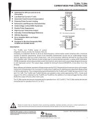
<strong>TL594</strong>Figure 1. Representative Block DiagramOutput Control13VCC68RTCT54DeadtimeControl+1–Oscillator≈ 0.12V≈ 0.7V0.7mA–+–+DeadtimeComparatorPWMComparator+2–+D QFlip–FlopCk Q–+UVLockout–3.5V4.9VReferenceRegulatorQ1Q29111012VCC1 2 3 15 16 14 7GndError Amp1Feedback PWMComparator InputError Amp2Ref.OutputThis device contains 46 active transistors.Capacitor CTFeedback/PWM Comp.Deadtime ControlFigure 2. Timing DiagramFlip–FlopClock InputFlip–FlopQFlip–FlopQOutput Q1EmitterOutput Q2EmitterOutputControl4 MOTOROLA ANALOG IC DEVICE DATA
<strong>TL594</strong>APPLICATIONS INFORMATIONDescriptionThe <strong>TL594</strong> is a fixed–frequency pulse width modulationcontrol circuit, incorporating the primary building blocksrequired for the control of a switching power supply. (SeeFigure 1.) An internal–linear sawtooth oscillator is frequency–programmable by two external components, RT and CT. Theapproximate oscillator frequency is determined by:fosc ≈ 1.1RT • CTFor more information refer to Figure 3.Output pulse width modulation is accomplished bycomparison of the positive sawtooth waveform acrosscapacitor CT to either of two control signals. The NOR gates,which drive output transistors Q1 and Q2, are enabled onlywhen the flip–flop clock–input line is in its low state. Thishappens only during that portion of time when the sawtoothvoltage is greater than the control signals. Therefore, anincrease in control–signal amplitude causes a correspondinglinear decrease of output pulse width. (Refer to the TimingDiagram shown in Figure 2.)The control signals are external inputs that can be fed intothe deadtime control, the error amplifier inputs, or thefeedback input. The deadtime control comparator has aneffective 120 mV input offset which limits the minimum outputdeadtime to approximately the first 4% of the sawtooth–cycletime. This would result in a maximum duty cycle on a givenoutput of 96% with the output control grounded, and 48% withit connected to the reference line. Additional deadtime maybe imposed on the output by setting the deadtime–controlinput to a fixed voltage, ranging between 0 V to 3.3 V.The pulse width modulator comparator provides a meansfor the error amplifiers to adjust the output pulse width fromthe maximum percent on–time, established by the deadtimecontrol input, down to zero, as the voltage at the feedback pinvaries from 0.5 V to 3.5 V. Both error amplifiers have aInput/OutputControlsFunctional TableOutput Functionfoutfosc =Grounded Single–ended PWM @ Q1 and Q2 1.0@ Vref Push–pull Operation 0.5common–mode input range from –0.3 V to (VCC – 2 V), andmay be used to sense power–supply output voltage andcurrent. The error–amplifier outputs are active high and areORed together at the noninverting input of the pulse–widthmodulator comparator. With this configuration, the amplifierthat demands minimum output on time, dominates control ofthe loop.When capacitor CT is discharged, a positive pulse isgenerated on the output of the deadtime comparator, whichclocks the pulse–steering flip–flop and inhibits the outputtransistors, Q1 and Q2. With the output–control connected tothe reference line, the pulse–steering flip–flop directs themodulated pulses to each of the two output transistorsalternately for push–pull operation. The output frequency isequal to half that of the oscillator. Output drive can also betaken from Q1 or Q2, when single–ended operation with amaximum on–time of less than 50% is required. This isdesirable when the output transformer has a ringbackwinding with a catch diode used for snubbing. When higheroutput–drive currents are required for single–endedoperation, Q1 and Q2 may be connected in parallel, and theoutput–mode pin must be tied to ground to disable theflip–flop. The output frequency will now be equal to that of theoscillator.The <strong>TL594</strong> has an internal 5.0 V reference capable ofsourcing up to 10 mA of load current for external bias circuits.The reference has an internal accuracy of ±1.5% with atypical thermal drift of less than 50 mV over an operatingtemperature range of 0° to 70°C.f OSC , OSCILLATOR FREQUENCY (Hz)500 k100 k10 kFigure 3. Oscillator Frequency versusTiming ResistanceCT = 0.001 µF0.01 µFVCC = 15 V0.1 µF1.0 k5001.0 k 2.0 k 5.0 k 10 k 20 k 50 k 100 k 200 k 500 k 1.0 MRT, TIMING RESISTANCE (Ω)VOL, OPEN LOOP VOLTAGE GAIN (dB)A120110100908070605040302010Figure 4. Open Loop Voltage Gain andPhase versus FrequencyAVOLVCC = 15 V∆VO = 3.0 VRL = 2.0 kΩ02040608010012014016001801.0 10 100 1.0 k 10 k 100 k 1.0 Mf, FREQUENCY (Hz)φ, EXCESS PHASE (DEGREES)φMOTOROLA ANALOG IC DEVICE DATA5