electro-tech.narod.ru, TL594
electro-tech.narod.ru, TL594
electro-tech.narod.ru, TL594
- No tags were found...

Create successful ePaper yourself
Turn your PDF publications into a flip-book with our unique Google optimized e-Paper software.
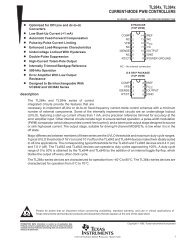
<strong>TL594</strong>RECOMMENDED OPERATING CONDITIONSCharacteristics Symbol Min Typ Max UnitPower Supply Voltage VCC 7.0 15 40 VCollector Output Voltage VC1, VC2 – 30 40 VCollector Output Current (Each transistor) IC1, IC2 – – 200 mAAmplified Input Voltage Vin 0.3 – VCC – 2.0 VCurrent Into Feedback Terminal lfb – – 0.3 mAReference Output Current lref – – 10 mATiming Resistor RT 1.8 30 500 kΩTiming Capacitor CT 0.0047 0.001 10 µFOscillator Frequency fosc 1.0 40 200 kHzPWM Input Voltage (Pins 3, 4, 13) – 0.3 – 5.3 VELECTRICAL CHARACTERISTICS (VCC = 15 V, CT = 0.01 µF, RT = 12 kΩ, unless otherwise noted.)For typical values TA = 25°C, for min/max values TA is the operating ambient temperature range that applies, unless otherwise noted.Characteristics Symbol Min Typ Max UnitREFERENCE SECTIONReference VoltageVrefV(IO = 1.0 mA, TA = 25°C)4.925 5.0 5.075(IO = 1.0 mA)4.9–5.1Line Regulation (VCC = 7.0 V to 40 V) Regline – 2.0 25 mVLoad Regulation (IO = 1.0 mA to 10 mA) Regload – 2.0 15 mVShort Circuit Output Current (Vref = 0 V) ISC 15 40 75 mAOUTPUT SECTIONCollector Off–State Current (VCC = 40 V, VCE = 40 V) IC(off) – 2.0 100 µAEmitter Off–State Current (VCC = 40 V, VC = 40 V, VE = 0 V) IE(off) – – –100 µACollector–Emitter Saturation Voltage (Note 2)VCommon–Emitter (VE = 0 V, IC = 200 mA)VSAT(C) –1.1 1.3Emitter–Follower (VC = 15 V, IE = –200 mA)VSAT(E) –1.5 2.5Output Control Pin CurrentLow State (VOC ≤ 0.4 V)High State (VOC = Vref)Output Voltage Rise TimeCommon–Emitter (See Figure 13)Emitter–Follower (See Figure 14)Output Voltage Fall TimeCommon–Emitter (See Figure 13)Emitter–Follower (See Figure 14)IOCLIOCHtrERROR AMPLIFIER SECTIONInput Offset Voltage (VO (Pin 3) = 2.5 V) VIO – 2.0 10 mVInput Offset Current (VO (Pin 3) = 2.5 V) IIO – 5.0 250 nAInput Bias Current (VO (Pin 3) = 2.5 V) IIB – –0.1 –1.0 µAInput Common Mode Voltage Range (VCC = 40 V, TA = 25°C) VICR 0 to VCC–2.0 VInverting Input Voltage Range VIR(INV) –0.3 to VCC–2.0 VOpen Loop Voltage Gain (∆VO = 3.0 V, VO = 0.5 V to 3.5 V, RL = 2.0 kΩ) AVOL 70 95 – dBUnity–Gain Crossover Frequency (VO = 0.5 V to 3.5 V, RL = 2.0 kΩ) fC – 700 – kHzPhase Margin at Unity–Gain (VO = 0.5 V to 3.5 V, RL = 2.0 kΩ) φm – 65 – deg.Common Mode Rejection Ratio (VCC = 40 V) CMRR 65 90 – dBPower Supply Rejection Ratio (∆VCC = 33 V, VO = 2.5 V, RL = 2.0 kΩ) PSRR – 100 – dBOutput Sink Current (VO (Pin 3) = 0.7 V) IO– 0.3 0.7 – mAOutput Source Current (VO (Pin 3) = 3.5 V) IO+ –2.0 –4.0 – mANOTE: 2. Low duty cycle pulse <strong>tech</strong>niques are used during test to maintain junction temperature as close to ambient temperature as possible.tf––––––0.12.01001004040–20200200100100µAnsns2 MOTOROLA ANALOG IC DEVICE DATA