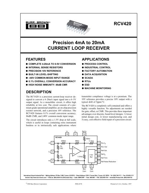
RCV420 Precision 4mA to 20mA CURRENT LOOP RECEIVER
RCV420 Precision 4mA to 20mA CURRENT LOOP RECEIVER
RCV420 Precision 4mA to 20mA CURRENT LOOP RECEIVER

You also want an ePaper? Increase the reach of your titles
YUMPU automatically turns print PDFs into web optimized ePapers that Google loves.
PIN CONFIGURATIONABSOLUTE MAXIMUM RATINGS (1)Top View–InC T+InV–123416151413V+Rcv fBRcv OutRcv ComDIPSupply ............................................................................................... ±22VInput Current, Continuous ................................................................ 40mAInput Current Momentary, 0.1s ........................... 250mA, 1% Duty CycleCommon-Mode Input Voltage, Continuous ....................................... ±40VLead Temperature (soldering, 10s) ............................................... +300°COutput Short Circuit <strong>to</strong> Common (Rcv and Ref) ..................... ContinuousNOTE: (1) Stresses above these ratings may cause permanent damage.Ref ComNCRef Noise ReductionRef Trim56781211109Ref InRef OutRef fBNCPACKAGE INFORMATIONPACKAGE DRAWINGPRODUCT PACKAGE NUMBER (1)<strong>RCV420</strong>KP 16-Pin Plastic DIP 180<strong>RCV420</strong>JP 16-Pin Plastic DIP 180NOTE: (1) For detailed drawing and dimension table, please see end of datasheet, or Appendix C of Burr-Brown IC Data Book.ORDERING INFORMATIONPERFORMANCEPRODUCT GRADE PACKAGE<strong>RCV420</strong>KP 0°C <strong>to</strong> +70°C 16-Pin Plastic DIP<strong>RCV420</strong>JP 0°C <strong>to</strong> +70°C 16-Pin Plastic DIPThe information provided herein is believed <strong>to</strong> be reliable; however, BURR-BROWN assumes no responsibility for inaccuracies or omissions. BURR-BROWN assumesno responsibility for the use of this information, and all use of such information shall be entirely at the user’s own risk. Prices and specifications are subject <strong>to</strong> changewithout notice. No patent rights or licenses <strong>to</strong> any of the circuits described herein are implied or granted <strong>to</strong> any third party. BURR-BROWN does not authorize or warrantany BURR-BROWN product for use in life support devices and/or systems.3<strong>RCV420</strong>®
TYPICAL PERFORMANCE CURVESAt T A= +25°C, V S= ±15V, unless otherwise noted.STEP RESPONSENO LOADSMALL SIGNAL RESPONSENO LOADSMALL SIGNAL RESPONSER L= ∞, C L= 1000pFPositive Common-Mode Range (V)8070605040POSITIVE COMMON-MODE VOLTAGE RANGEvs POSITIVE POWER SUPPLY VOLTAGET A = +25°CT A = –55°CT A = +125°CMax Rating = 40V–V S = –5V <strong>to</strong> –20V3011 12 13 14 15 16 17 18 19 2011.4 Positive Power Supply Voltage (V)Negative Common-Mode Range (V)–80–70–60–50–40–30–20NEGATIVE COMMON-MODE VOLTAGE RANGEvs NEGATIVE POWER SUPPLY VOLTAGEMax Rating = –40VT A = +25°CT A = –55°C <strong>to</strong> +125°C+V S = +11.4V <strong>to</strong> +20V–10–5 –10 –15–20Negative Power Supply Voltage (V)100COMMON-MODE REJECTIONvs FREQUENCY100POWER-SUPPLY REJECTIONvs FREQUENCY908080CMR (dB)60PSR (dB)60V+ V–401 10 100 1k 10k 100kFrequency (Hz)401 10 100 1k 10k 100kFrequency (Hz)®<strong>RCV420</strong>4
THEORY OF OPERATIONRefer <strong>to</strong> the figure on the first page. For 0 <strong>to</strong> 5V output with4–<strong>20mA</strong> input, the required transimpedance of the circuit is:V OUT /I IN = 5V/16mA = 0.3125V/mA.To achieve the desired output (0V for <strong>4mA</strong> and 5V for<strong>20mA</strong>), the output of the amplifier must be offset by anamount:V OS = –(<strong>4mA</strong>)(0.3125V/mA) = –1.25V.The input current signal is connected <strong>to</strong> either +In or –In,depending on the polarity of the signal, and returned <strong>to</strong>ground through the center tap, C T . The balanced input—twomatched 75Ω sense resis<strong>to</strong>rs, R S —provides maximum rejectionof common-mode voltage signals on C T and true differentialcurrent-<strong>to</strong>-voltage conversion. The sense resis<strong>to</strong>rsconvert the input current signal in<strong>to</strong> a proportional voltage,which is amplified by the differential amplifier. The voltagegain of the amplifier is:A D = 5V/(16mA)(75Ω) = 4.1667V/V.The tee network in the feedback path of the amplifierprovides a summing junction used <strong>to</strong> generate the required–1.25V offset voltage. The input resis<strong>to</strong>r network provideshigh-input impedance and attenuates common-mode inputvoltages <strong>to</strong> levels suitable for the operational amplifier’scommon-mode signal capabilities.necessary level shifting. If the Ref In pin is not used for levelshifting, then it must be grounded <strong>to</strong> maintain high CMR.GAIN AND OFFSET ADJUSTMENTFigure 2 shows the circuit for adjusting the <strong>RCV420</strong> gain.Increasing the gain of the <strong>RCV420</strong> is accomplished byinserting a small resis<strong>to</strong>r in the feedback path of the amplifier.Increasing the gain using this technique results in CMRdegradation, and therefore, gain adjustments should be keptas small as possible. For example, a 1% increase in gain istypically realized with a 125Ω resis<strong>to</strong>r, which degradesCMR by about 6dB.A decrease in gain can be achieved by placing matchedresis<strong>to</strong>rs in parallel with the sense resis<strong>to</strong>rs, also shown inFigure 2. The adjusted gain is given by the followingexpressionV OUT /I IN = 0.3125 x R X /(R X + R S ).A 1% decrease in gain can be achieved with a 7.5kΩresis<strong>to</strong>r. It is important <strong>to</strong> match the parallel resistance oneach sense resis<strong>to</strong>r <strong>to</strong> maintain high CMR. The TCR mismatchbetween the two external resis<strong>to</strong>rs will effect gainerror drift and CMR drift.There are two methods for nulling the <strong>RCV420</strong> output offsetvoltage. The first method applies <strong>to</strong> applications using theinternal 10V reference for level shifting. For these applica-BASIC POWER SUPPLYAND SIGNAL CONNECTIONSFigure 1 shows the proper connections for power supply andsignal. Both supplies should be decoupled with 1µF tantalumcapaci<strong>to</strong>rs as close <strong>to</strong> the amplifier as possible. To avoidgain and CMR errors introduced by the external circuit,connect grounds as indicated, being sure <strong>to</strong> minimize groundresistance. The input signal should be connected <strong>to</strong> either+In or –In, depending on its polarity, and returned <strong>to</strong> groundthrough the center tap, C T . The output of the voltage reference,Ref Out, should be connected <strong>to</strong> Ref In for the10kΩ (1) 3–In1 15+InR X200Ω (1)10kΩ (1) RC XT 2<strong>RCV420</strong>14FIGURE 2. Optional Gain Adjustment.R 1±0.5% GainAdjustmentRcv OutNOTE: (1) Typical values. See text.I IN4–<strong>20mA</strong>C T+In 32–In 1R SR S75Ω75Ω<strong>RCV420</strong>+10VReference12 Ref In15 Rcv fB14 Rcv Out11 Ref Out10 Ref f B8 Ref Trim7 Ref Noise ReductionV O(0–5V)V+ 16 4 V–1µF 1µF13Rcv Com5Ref ComFIGURE 1. Basic Power Supply and Signal Connections.5<strong>RCV420</strong>®
tions, the voltage reference output trim procedure can beused <strong>to</strong> null offset errors at the output of the <strong>RCV420</strong>. Thevoltage reference trim circuit is discussed under “VoltageReference.”When the voltage reference is not used for level shifting orwhen large offset adjustments are required, the circuit inFigure 3 can be used for offset adjustment. A low impedanceon the Rcv Com pin is required <strong>to</strong> maintain high CMR.ZERO ADJUSTMENTLevel shifting the <strong>RCV420</strong> output voltage can be achievedusing either the Ref In pin or the Rcv Com pin. Thedisadvantage of using the Ref In pin is that there is an 8:1voltage attenuation from this pin <strong>to</strong> the output of the <strong>RCV420</strong>.Thus, use the Rcv Com pin for large offsets, because thevoltage on this pin is seen directly at the output. Figure 4shows the circuit used <strong>to</strong> level-shift the output of the <strong>RCV420</strong>–In1C T 2+In 312<strong>RCV420</strong>1315±150mV adjustment at output.514OPA237VO100kΩ1kΩ+15V–15V100kΩFIGURE 3. Optional Output Offset Nulling Using ExternalAmplifier.using the Rcv Com pin. It is important <strong>to</strong> use a low-outputimpedance amplifier <strong>to</strong> maintain high CMR. With this methodof zero adjustment, the Ref In pin must be connected <strong>to</strong> theRcv Com pin.MAINTAINING COMMON-MODE REJECTIONTwo fac<strong>to</strong>rs are important in maintaining high CMR: (1)resis<strong>to</strong>r matching and tracking (the internal resis<strong>to</strong>r networkdoes this) and (2) source impedance. CMR depends on theaccurate matching of several resis<strong>to</strong>r ratios. The high accuraciesneeded <strong>to</strong> maintain the specified CMR and CMRtemperature coefficient are difficult and expensive <strong>to</strong> reliablyachieve with discrete components. Any resistance imbalanceintroduced by external circuitry directly affectsCMR. These imbalances can occur by: mismatching senseresis<strong>to</strong>rs when gain is decreased, adding resistance in thefeedback path when gain is increased, and adding seriesresistance on the Rcv Com pin.The two sense resis<strong>to</strong>rs are laser-trimmed <strong>to</strong> typically matchwithin 0.01%; therefore, when adding parallel resistance <strong>to</strong>decrease gain, take care <strong>to</strong> match the parallel resistance oneach sense resis<strong>to</strong>r. To maintain high CMR when increasingthe gain of the <strong>RCV420</strong>, keep the series resistance added <strong>to</strong>the feedback network as small as possible. Whether the RcvCom pin is grounded or connected <strong>to</strong> a voltage reference forlevel shifting, keep the series resistance on this pin as low aspossible. For example, a resistance of 20Ω on this pindegrades CMR from 86dB <strong>to</strong> approximately 80dB. Forapplications requiring better than 86dB CMR, the circuitshown in Figure 5 can be used <strong>to</strong> adjust CMR.PROTECTING THE SENSE RESISTORThe 75Ω sense resis<strong>to</strong>rs are designed for a maximum continuouscurrent of 40mA, but can withstand as much as250mA for up <strong>to</strong> 0.1s (see absolute maximum ratings).There are several ways <strong>to</strong> protect the sense resis<strong>to</strong>r from–In1C T 2+In 312V ZERO±5V adjustmentat output.<strong>RCV420</strong>135OPA2371015141110kΩ10kΩ+10VUse 10V Ref for +and 10V Ref with INA105 for –.V O = (0.3125)(I IN ) + V ZEROVO2 5INA1053150kΩ6–10V<strong>RCV420</strong>131kΩ1kΩOPA2371kΩ1kΩProcedure:1. Connect CMV <strong>to</strong> CT .2. Adjust potentiometer for near zeroat the output.200ΩCMRAdjustFIGURE 4. Optional Zero Adjust Circuit.FIGURE 5. Optional Circuit for Externally Trimming CMR.®<strong>RCV420</strong>6
overcurrent conditions exceeding these specifications. Refer<strong>to</strong> Figure 6. The simplest and least expensive method is aresis<strong>to</strong>r as shown in Figure 6a. The value of the resis<strong>to</strong>r isdetermined from the expressionR X = V CC /40mA – 75Ωand the full scale voltage drop isV RX = <strong>20mA</strong> x R X .V+V RX R X 4–<strong>20mA</strong>32115<strong>RCV420</strong>14VOFor a system operating off of a 32V supply R X = 725Ω andV RX = 14.5V. In applications that cannot <strong>to</strong>lerate such alarge voltage drop, use circuits 6b or 6c. In circuit 6b apower JFET and source resis<strong>to</strong>r are used as a current limit.The 200Ω potentiometer, R X , is adjusted <strong>to</strong> provide a currentlimit of approximately 30mA. This circuit introduces a1–4V drop at full scale. If only a very small series voltagedrop at full scale can be <strong>to</strong>lerated, then a 0.032A series 217fast-acting fuse should be used, as shown in Figure 6c.For au<strong>to</strong>matic fold-back protection, use the circuit shown inFigure 15.V+R Xa) R X = (V+)/40mA – 75Ω2N3970200Ω4–<strong>20mA</strong>3152<strong>RCV420</strong>114VOVOLTAGE REFERENCEThe <strong>RCV420</strong> contains a precision 10V reference. Figure 8shows the circuit for output voltage adjustment. Trimmingthe output will change the voltage drift by approximately0.007ppm/°C per mV of trimmed voltage. Any mismatch inTCR between the two sides of the potentiometer will alsoaffect drift, but the effect is divided by approximately 5. Thetrim range of the voltage reference using this method istypically ±400mV. The voltage reference trim can be used <strong>to</strong>trim offset errors at the output of the <strong>RCV420</strong>. There is an8:1 voltage attenuation from Ref In <strong>to</strong> Rcv Out, and thus thetrim range at the output of the receiver is typically ±50mV.The high-frequency noise (<strong>to</strong> 1MHz) of the voltage referenceis typically 1mVp-p. When the voltage reference isused for level shifting, its noise contribution at the output ofthe receiver is typically 125µVp-p due <strong>to</strong> the 8:1 attenuationfrom Ref In <strong>to</strong> Rcv Out. The reference noise can be reducedby connecting an external capaci<strong>to</strong>r between the NoiseReduction pin and ground. For example, 0.1µF capaci<strong>to</strong>rreduces the high-frequency noise <strong>to</strong> about 200µVp-p at theoutput of the reference and about 25µVp-p at the output ofthe receiver.–InV+f 112C T3b) R X set for 30mA current limit at 25°C.4–<strong>20mA</strong>321<strong>RCV420</strong><strong>RCV420</strong>c) f 1 is 0.032A, Lifflefuse Series 217 fast-acting fuse.Request Application Bulletin AB-014 for details of amore complete protection circuit.FIGURE 6. Protecting the Sense Resis<strong>to</strong>rs.15151414VOVO+In10118V REF20kΩ±400mV adjustment at output of reference, and ±50mVadjustment at output of receiver if reference is used forlevel shifting.FIGURE 7. Optional Voltage Reference External Trim Circuit.7<strong>RCV420</strong>®
Pt100100°C <strong>to</strong>600°CRTDR LIN15760ΩR Z137Ω134R G402Ω321211N4148V LIN I 14+ R1 11V INI R2 10 VREGV+R GB 9XTR105Q 1 0.01µFE 8R GI O–V IN 7I RET6I O = <strong>4mA</strong> – <strong>20mA</strong>+12V1µF1610113 1215<strong>RCV420</strong>14213541µFV O = 0 <strong>to</strong> 5V–12VR CM = 1kΩ0.01µFNOTE: A two-wire RTD connection is shown. For remotelylocated RTDs, a three-wire RTD conection is recommended.R G becomes 383Ω, R LIN2 is 8060Ω. See Figure 3 andTable I.FIGURE 8. <strong>RCV420</strong> Used in Conjunction with XTR101 <strong>to</strong> Form a Complete Solution for 4-<strong>20mA</strong> Loop.RTDR LIN1R ZR LIN2134R G32V IN+V LIN I R1I R2 10 VREGV+R G9BXTR105E8R GI O–V IN 7I RET612114 11Q 1I O = <strong>4mA</strong> – <strong>20mA</strong>1N41480.01µFNOTE: A three-wire RTD connection is shown.For a two-wire RTD connection eliminate R LIN2 .1610113 12<strong>RCV420</strong>2135415141µF1µF115ISO12216 2+15VIsolated Power0from PWS740–15V910 8 7V+V O0 – 5VV–R CM = 1kΩ0.01µFFIGURE 9. Isolated 4-<strong>20mA</strong> Instrument Loop (RTD shown).®<strong>RCV420</strong>8
4–<strong>20mA</strong>+In 3C T 2–In 110R SR S1112<strong>RCV420</strong>(1)1351514V O(0–5V)3214–<strong>20mA</strong>C T1215<strong>RCV420</strong>1051314 VO(5–0V)11+10V12kΩ10+6.25VOPA237+6.25V20kΩ+In31112R G(1)C T1–In2R SR S<strong>RCV420</strong>(N)131514V O(0–5V)V O = 6.25V – (0.3125) (I IN )FIGURE 12. 4-<strong>20mA</strong> <strong>to</strong> 5-0V Conversion.R CM(1)5I LNOTE: (1) R CM and R G are used <strong>to</strong> provide a first order correction of CMRand Gain Error, respectively. Table 1 gives typical resis<strong>to</strong>r values for R CMand R G when as many as three <strong>RCV420</strong>s are stacked. Table II givestypical CMR and Gain Error with no correction. Further improvement inCMR and Gain Error can be achieved using a 500kΩ potentiometer forR CM and a 100Ω potentiometer for R G .<strong>RCV420</strong> R CM (kΩ) R G (Ω)1 ∞ 02 200 73 67 23TABLE 1. Typical Values for R CM and R G .R X(1)LoadPower Supply–40V (max)+40V (max)+InR 15SC T 2<strong>RCV420</strong>+In3R (1)X1R S5121314V O (0-5V)<strong>RCV420</strong> CMR (dB) GAIN ERROR %1 94 0.0252 68 0.0753 62 0.200TABLE II. Typical CMR and Gain ErrorWithout Correction.FIGURE 10. Series 4-<strong>20mA</strong> Receivers.R X(1)PowerSupplyLoad+In15R (1)C X R ST–InR S5<strong>RCV420</strong>121314V O (0-5V)I LI 1+InC T132R S<strong>RCV420</strong>1514V O( I L MAXNOTE: (1) R X= R S/ –116mA )FIGURE 13. Power Supply Current Moni<strong>to</strong>r Circuit.I 2 R–InS13125V O= 0.3125 (I 1– I 2)Max Gain Error = 0.1% (<strong>RCV420</strong>BG)FIGURE 11. Differential Current-<strong>to</strong>-Voltage Converter.9<strong>RCV420</strong>®
+15V–15V16 41300kΩ<strong>RCV420</strong>99kΩ92kΩ122375Ω75Ω300kΩ1.01kΩ100kΩ11.5kΩ10.0VReference1514101110.0V1.27kΩV OUT0–5V+5V13 58+15V10kΩAT&TLH1191Solid-StateRelay8 41MΩ 10kΩ 10kΩ726555Timer51µF 0.01µF3 1LM19310kΩ10kΩ6.95V4–<strong>20mA</strong>Input1µF470Ω47kΩ2N390440.57V604Ω22.9kΩOverrangeOutputUnderrangeOutputSee Application Bulletin AB-014 for more details.FIGURE 14. 4-<strong>20mA</strong> Current Loop Receiver with Input Overload Protection.+15V –15V16 41<strong>RCV420</strong>12301Ω300kΩ75Ω99kΩ92kΩ15V O0-<strong>20mA</strong>Input301Ω2375Ω300kΩ100kΩ1.01kΩ11.5kΩ10.0VRef1410110-5V135See Application Bulletin AB-018 for more details.FIGURE 15. 0-<strong>20mA</strong>/0-5V Receiver Using <strong>RCV420</strong>.®<strong>RCV420</strong>10