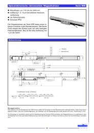
PhotoMOS Relay Schematic and Wiring Diagrams
PhotoMOS Relay Schematic and Wiring Diagrams
PhotoMOS Relay Schematic and Wiring Diagrams

Create successful ePaper yourself
Turn your PDF publications into a flip-book with our unique Google optimized e-Paper software.
<strong>PhotoMOS</strong> <strong>Relay</strong> <strong>Schematic</strong> <strong>and</strong> <strong>Wiring</strong> <strong>Diagrams</strong>Type<strong>Schematic</strong>LoadOutputconfigurationConnection<strong>Wiring</strong> diagram166LoadAC/DCAE1IF2354ILVL (AC,DC)4ILVL (AC,DC)LoadAQV21AQV21 (SOP)AQV22AQV22 (SOP)AQV23AQV25Series1236541a DC B*E1E1IFIF1231236 Load +54654ILILLoadVL (DC)––VL (DC)+6 +IL5 VL (DC)Load–5 Load –4 IL VL (DC)+123654DCCE1IF123654LoadIL+VL (DC)–654ILLoad+VL (DC)–(AQV254R only)(1) Two independent 1 Form A use188LoadAQW21AQW21❍EHAQW21 (SOP)AQW22AQW25AQW27Series123487652a AC/DC —E1IF1E1IF2234(2) 2 Form A use12E1 IF 3765876IL1IL2IL1LoadLoadLoadVL1 (AC,DC)VL2 (AC,DC)VL1 (AC,DC)765876IL1IL2IL1LoadLoadLoadVL1 (AC,DC)VL2 (AC,DC)VL1 (AC,DC)45IL2VL2 (AC,DC)5IL2VL2 (AC,DC)LoadAQW21❍TSSeries+ 1– 2+ 3– 4<strong>Relay</strong> portion(1,2,7,8 pins)Detector portion(3,4,5,6 pins)8765<strong>Relay</strong>portion1aDetecterportion1a<strong>Relay</strong>portionAC/DCDetecterportionDC—E1+(DC)VL2–IF1LoadIL212348765IL1IF2LoadE2VL1(AC,DC)8765LoadIL1IF2VL1(AC,DC)E2AQW21❍T2SSeries+1 12–211+310–49+58–67<strong>Relay</strong> portion(1,2,11,12 pins)Detector portion(3,4,9,10 pins)(5,6,7,8 pins)<strong>Relay</strong>portion1aDetecterportion2a<strong>Relay</strong>portionAC/DCDetecterportionDC—E11IF12+Load 3(DC)VL2–IL24+Load 5(DC)VL3–IL3612111098IL1IF27IF3LoadE2E3VL1(AC,DC)121110987LoadIL1IF2IF3VL1(AC,DC)*Can be also connected as 2 Form A type. (However, the sum of the continuous load current should not exceed the absolute maximum rating.)**Can be also connected as 2 Form B type. (However, the sum of the continuous load current should not exceed the absolute maximum rating.)Notes: 1. E 1 : Power source at input side; V IN : Input voltage; I F : LED forward current; I IN : Input current; V L : Load voltage; I L : Load current; R: Current limit resistor.2. Method of connecting the load at the output is divided into 3 types.E2E326
Type<strong>Schematic</strong>LoadOutputconfigurationConnection<strong>Wiring</strong> diagram116215AQS210PSSeries34567814131211109<strong>Relay</strong> portion(2,3,15,16 pins)Detector portion(7,8,9,10 pins)Bridge rectifier portion(10,11,12,15 pins)Darlington portion(12,13,14 pins)<strong>Relay</strong> <strong>Relay</strong>portion portion1a AC/DCDetector Detectorportion portion1a DC—E112IF1 3456Load 7(DC)VL2IL2 8161514131211109LoadIL1IF2VL1 (AC,DC)E21615109LoadIL1IF2VL1 (AC,DC)E2116AQS210TSSeries23456781514131211109<strong>Relay</strong> portion(2,3,14,15,16 pins)(4,5,11,12,13 pins)Detector portion(6,7,9,10 pins)<strong>Relay</strong> <strong>Relay</strong>portion portion2a AC/DCDetector Detectorportion portion1a DC—E1E2(DC)VL312IF1 34IF2 56IL3 7Load 8161514131211109IL1LoadIL2LoadIF3VL1 (AC,DC)VL2 (AC,DC)E316141311109LoadIL1LoadIL2IF2VL1 (AC,DC)VL2 (AC,DC)E3116AQS210T2SSeries23456781514131211109<strong>Relay</strong> portion(2,3,14,15,16 pins)Detector portion(4,5,11,12 pins)(6,7,9,10 pins)<strong>Relay</strong> <strong>Relay</strong>portion portion1a AC/DCDetector Detectorportion portion2a DC—E1 IF1(DC)VL2 IL2Load(DC)VL3 IL3Load12345678161514131211109IL1LoadIF2IF3VL1 (AC,DC)E2E316141211109LoadIL1IF2IF3VL1 (AC,DC)E2E3166LoadAC/DCAE1IF2354ILVL (AC,DC)4ILVL (AC,DC)LoadAQV41AQV41 (SOP)AQV45Series1236541bDCB**E1E1IFIF1231236 Load +54654ILILLoadVL (DC)––VL (DC)+6 +IL5 VL (DC)Load–5 Load –4 IL VL (DC)+DCCE1IF123654LoadIL+VL (DC)–654ILLoad+VL (DC)–*Can be also connected as 2 Form A type. (However, the sum of the continuous load current should not exceed the absolute maximum rating.)**Can be also connected as 2 Form B type. (However, the sum of the continuous load current should not exceed the absolute maximum rating.)Notes: 1. E 1 : Power source at input side; V IN : Input voltage; I F : LED forward current; I IN : Input current; V L : Load voltage; I L : Load current; R: Current limit resistor.2. Method of connecting the load at the output is divided into 3 types.27
Type<strong>Schematic</strong>LoadOutputconfigurationConnection<strong>Wiring</strong> diagram(1) Two independent 1 Form A & 1 Form B use188LoadAQW61AQW61❍EHAQW65Series1234N.C.N.O.87651a1b AC/DC —E1IF1E1IF2273465(2) 1 Form A 1 Form B use1827E1 IF 36IL1IL2IL1LoadLoadLoadVL1 (AC,DC)VL2 (AC,DC)VL1 (AC,DC)765876IL1IL2IL1LoadLoadLoadVL1 (AC,DC)VL2 (AC,DC)VL1 (AC,DC)45IL2VL2 (AC,DC)5IL2VL2 (AC,DC)Load(1) Two independent 1 Form B use188LoadE1IF12376IL1LoadVL1 (AC,DC)76IL1LoadVL1 (AC,DC)AQW41AQW41❍EHAQW45Series123487652b AC/DC —E1IF24(2) 2 Form B use158IL2LoadVL2 (AC,DC)58IL2LoadVL2 (AC,DC)2E1 IF 376IL1LoadVL1 (AC,DC)76IL1LoadVL1 (AC,DC)45IL2VL2 (AC,DC)5IL2VL2 (AC,DC)LoadAQV10Series123654Terminal 3 cannot beused, since it is in the internalcircuit of the relay.1a DC AE1IF123654ILLoad–VL (DC)+64LoadIL–VL (DC)+166LoadAC/DCAVINIF2354ILVL (AC,DC)4ILVL (AC,DC)LoadAQV20Series1236541a DC B*VINVINIFIF1231236 Load +54654ILILLoadVL (DC)––VL (DC)+6 +IL5 VL (DC)Load–5 Load –4 IL VL (DC)+Terminal 3 cannot beused, since it is in the internalcircuit of the relay.DCCVINIF123654LoadIL+VL (DC)–654ILLoad+VL (DC)–*Can be also connected as 2 Form A type. (However, the sum of the continuous load current should not exceed the absolute maximum rating.)**Can be also connected as 2 Form B type. (However, the sum of the continuous load current should not exceed the absolute maximum rating.)Notes: 1. E 1 : Power source at input side; V IN : Input voltage; I F : LED forward current; I IN : Input current; V L : Load voltage; I L : Load current; R: Current limit resistor.2. Method of connecting the load at the output is divided into 3 types.28
Type<strong>Schematic</strong>LoadOutputconfigurationConnection<strong>Wiring</strong> diagramAQX21•44Series(Multichanneltype)123456789101112131 Input Common: DC+2 Input 1: DC–3 Input 2: DC–4 Input 3: DC–5 Input 4: DC–6 Output 1 (N.O.):DC or AC7 Output 1 (N.O.):DC or AC8 Output 2 (N.O.):DC or AC9 Output 2 (N.O.):DC or AC10 Output 3 (N.O.):DC or AC11 Output 3 (N.O.):DC or AC12 Output 4 (N.O.):DC or AC13 Output 4 (N.O.):DC or AC4a AC/DC –E1IF1 R12IF2R 3IF3R 4IF4R 5678IL1Load10 Load12 LoadLoadVL1 (AC,DC)IL2 VL29 (AC,DC)IL3 VL311 (AC,DC)IL4 VL413 (AC,DC)678910111213LoadIL1LoadIL2LoadIL3LoadIL4VL1 (AC,DC)VL2 (AC,DC)VL3 (AC,DC)VL4 (AC,DC)AQY21(SOP)AQY21❍EHAQY22(SOP)AQY27Series12431a AC/DC –E1IF142 3ILLoadVL (AC,DC)43LoadILVL (AC,DC)AQY41(SOP)AQY41❍EHSeries12431b AC/DC –E1IF142 3ILLoadVL (AC,DC)43LoadILVL (AC,DC)AQZ20AQZ26Series1 2 3 4– +1aAC/DC1 2 3 4IFE1R3 4ILILLoadVL (AC or DC)VL (AC or DC)LoadAQZ10Series1 2 3 4– + – +1aDC1 2 3 4IFE1R3 4ILILLoadLoad+VL (DC)–+VL (DC)–*Can be also connected as 2 Form A type. (However, the sum of the continuous load current should not exceed the absolute maximum rating.)**Can be also connected as 2 Form B type. (However, the sum of the continuous load current should not exceed the absolute maximum rating.)Notes: 1. E 1 : Power source at input side; V IN : Input voltage; I F : LED forward current; I IN : Input current; V L : Load voltage; I L : Load current; R: Current limit resistor.2. Method of connecting the load at the output is divided into 3 types.29
Type<strong>Schematic</strong>OutputconfigurationLoad<strong>Wiring</strong> diagramAQZ40Series1bAC/DC1 2 3 4LoadIF R ILVL (AC or DC)1 2 3 4– +E13 4ILVL (AC or DC)LoadAQZ20·VSeries1 2 3 4– +1aAC/DC1 2 3 4IFE1R3 4ILILLoadVL (AC or DC)VL (AC or DC)LoadAQZ20·DSeries1aAC/DC1 2 3 4IINILLoadVL (AC or DC)1 2 3 4– +VIN3 4ILVL (AC or DC)LoadAQZ10·DSeries1 2 3 4– + – +1aDC1 2 3 4IINVIN3 4ILILLoadLoad+VL (DC)–+VL (DC)–Notes: 1. E 1 : Power source at input side; V IN : Input voltage; I F : LED forward current; I IN : Input current; V L : Load voltage; I L : Load current; R: Current limit resistor.2. Method of connecting the load at the output is divided into 3 types.30