82C54 Counter/Timer IC Datasheet - Diamond Systems Corporation
82C54 Counter/Timer IC Datasheet - Diamond Systems Corporation
82C54 Counter/Timer IC Datasheet - Diamond Systems Corporation

You also want an ePaper? Increase the reach of your titles
YUMPU automatically turns print PDFs into web optimized ePapers that Google loves.
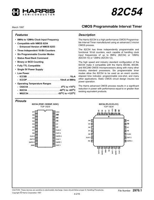
SEM<strong>IC</strong>ONDUCTOR<strong>82C54</strong>March 1997CMOS Programmable Interval <strong>Timer</strong>Features• 8MHz to 12MHz Clock Input Frequency• Compatible with NMOS 8254- Enhanced Version of NMOS 8253• Three Independent 16-Bit <strong>Counter</strong>s• Six Programmable <strong>Counter</strong> Modes• Status Read Back Command• Binary or BCD Counting• Fully TTL Compatible• Single 5V Power Supply• Low Power- <strong>IC</strong>CSB . . . . . . . . . . . . . . . . . . . . . . . . . . . . . . . . . .10µA- <strong>IC</strong>COP . . . . . . . . . . . . . . . . . . . . . . . . . . 10mA at 8MHz• Operating Temperature Ranges- C<strong>82C54</strong> . . . . . . . . . . . . . . . . . . . . . . . . . .0 o C to +70 o C- I<strong>82C54</strong> . . . . . . . . . . . . . . . . . . . . . . . . . -40 o C to +85 o C- M<strong>82C54</strong> . . . . . . . . . . . . . . . . . . . . . . . -55 o C to +125 o CDescriptionThe Harris <strong>82C54</strong> is a high performance CMOS ProgrammableInterval <strong>Timer</strong> manufactured using an advanced 2 micronCMOS process.The <strong>82C54</strong> has three independently programmable andfunctional 16-bit counters, each capable of handling clockinput frequencies of up to 8MHz (<strong>82C54</strong>) or 10MHz(<strong>82C54</strong>-10) or 12MHz (<strong>82C54</strong>-12).The high speed and industry standard configuration of the<strong>82C54</strong> make it compatible with the Harris 80C86, 80C88,and 80C286 CMOS microprocessors along with many otherindustry standard processors. Six programmable timermodes allow the <strong>82C54</strong> to be used as an event counter,elapsed time indicator, programmable one-shot, and manyother applications. Static CMOS circuit design insures lowpower operation.The Harris advanced CMOS process results in a significantreduction in power with performance equal to or greater thanexisting equivalent products.Pinouts<strong>82C54</strong> (PDIP, CERDIP, SO<strong>IC</strong>)TOP VIEW<strong>82C54</strong> (PLCC/CLCC)TOP VIEWD7D6122423VCCWRD5D6D7NCVCCWRRD4 3 2 1 28 27 26D5322RDD4421CSD4525NCD3520A1D3624CSD2619A0D2723D1 7D0 8CLK 0 9OUT 0 10GATE 0 111817161514CLK 2OUT 2GATE 2CLK 1GATE 1GND 1213OUT 1OUT 0GATE 0GNDNCOUT 1GATE 1CLK 1A1D1D0CLK 0NC89101122212019A0CLK2OUT 2GATE 212 13 14 15 16 17 18CAUTION: These devices are sensitive to electrostatic discharge. Users should follow proper <strong>IC</strong> Handling Procedures.Copyright © Harris <strong>Corporation</strong> 19974-215File Number 2970.1
<strong>82C54</strong>Ordering InformationPART NUMBERSTEMPERATURE8MHz 10MHz 12MHzRANGE PACKAGE PKG. NO.CP<strong>82C54</strong> CP<strong>82C54</strong>-10 CP<strong>82C54</strong>-12 0 o C to +70 o C 24 Lead PDIP E24.6IP<strong>82C54</strong> IP<strong>82C54</strong>-10 IP<strong>82C54</strong>-12 -40 o C to +85 o C 24 Lead PDIP E24.6CS<strong>82C54</strong> CS<strong>82C54</strong>-10 CS<strong>82C54</strong>-12 0 o C to +70 o C 28 Lead PLCC N28.45IS<strong>82C54</strong> IS<strong>82C54</strong>-10 IS<strong>82C54</strong>-12 -40 o C to +85 o C 28 Lead PLCC N28.45CD<strong>82C54</strong> CD<strong>82C54</strong>-10 CD<strong>82C54</strong>-12 0 o C to +70 o C 24 Lead CERDIP F24.6ID<strong>82C54</strong> ID<strong>82C54</strong>-10 ID<strong>82C54</strong>-12 -40 o C to +85 o C 24 Lead CERDIP F24.6MD<strong>82C54</strong>/B MD<strong>82C54</strong>-10/B MD<strong>82C54</strong>-12/B -55 o C to +125 o C 24 Lead CERDIP F24.6MR<strong>82C54</strong>/B MR<strong>82C54</strong>-10/B MR<strong>82C54</strong>-12/B -55 o C to +125 o C 28 Lead CLCC J28.ASMD # 8406501JA - 8406502JA -55 o C to +125 o C 24 Lead CERDIP F24.6SMD# 84065013A - 84065023A -55 o C to +125 o C 28 Lead CLCC J28.ACM<strong>82C54</strong> CM<strong>82C54</strong>-10 CM<strong>82C54</strong>-12 0 o C to +70 o C 24 Lead SO<strong>IC</strong> M24.3Functional DiagramD 7 - D 08DATA/BUSBUFFERCOUNTER0CLK 0GATE 0OUT 0INTERNAL BUSCONTROLWORDREGISTERSTATUSLATCHCR MCR LRDWRA 0A 1CSREAD/WRITELOG<strong>IC</strong>INTERNAL BUSCOUNTER1CLK 1GATE 1OUT 1CONTROLLOG<strong>IC</strong>STATUSREGISTERCECONTROLWORDREGISTERCOUNTER2CLK 2GATE 2OUT 2OL MOL LGATE nCLK nOUT nCOUNTER INTERNAL BLOCK DIAGRAMPin DescriptionSYMBOLDIP PINNUMBER TYPE DEFINITIOND7 - D0 1 - 8 I/O DATA: Bi-directional three-state data bus lines, connected to system data bus.CLK 0 9 I CLOCK 0: Clock input of <strong>Counter</strong> 0.OUT 0 10 O OUT 0: Output of <strong>Counter</strong> 0.GATE 0 11 I GATE 0: Gate input of <strong>Counter</strong> 0.GND 12 GROUND: Power supply connection.OUT 1 13 O OUT 1: Output of <strong>Counter</strong> 1.GATE 1 14 I GATE 1: Gate input of <strong>Counter</strong> 1.CLK 1 15 I CLOCK 1: Clock input of <strong>Counter</strong> 1.GATE 2 16 I GATE 2: Gate input of <strong>Counter</strong> 2.OUT 2 17 O OUT 2: Output of <strong>Counter</strong> 2.4-216
<strong>82C54</strong>Pin Description (Continued)SYMBOLDIP PINNUMBER TYPE DEFINITIONCLK 2 18 I CLOCK 2: Clock input of <strong>Counter</strong> 2.A0, A1 19 - 20 I ADDRESS: Select inputs for one of the three counters or Control Word Register for read/writeoperations. Normally connected to the system address bus.A1 A0 SELECTS0 0 <strong>Counter</strong> 00 1 <strong>Counter</strong> 11 0 <strong>Counter</strong> 21 1 Control Word RegisterCS 21 I CHIP SELECT: A low on this input enables the <strong>82C54</strong> to respond to RD and WR signals. RD andWR are ignored otherwise.RD 22 I READ: This input is low during CPU read operations.WR 23 I WRITE: This input is low during CPU write operations.V CC 24 V CC : The +5V power supply pin. A 0.1µF capacitor between pins VCC and GND is recommendedfor decoupling.Functional DescriptionGeneralThe <strong>82C54</strong> is a programmable interval timer/counterdesigned for use with microcomputer systems. It is a generalpurpose, multi-timing element that can be treated as anarray of I/O ports in the system software.D 7 - D 08DATA/BUSBUFFERCOUNTER0CLK 0GATE 0OUT 0The <strong>82C54</strong> solves one of the most common problems in anymicrocomputer system, the generation of accurate timedelays under software control. Instead of setting up timingloops in software, the programmer configures the <strong>82C54</strong> tomatch his requirements and programs one of the countersfor the desired delay. After the desired delay, the <strong>82C54</strong> willinterrupt the CPU. Software overhead is minimal and variablelength delays can easily be accommodated.Some of the other computer/timer functions common to microcomputerswhich can be implemented with the <strong>82C54</strong> are:• Real time clock• Event counter• Digital one-shot• Programmable rate generator• Square wave generator• Binary rate multiplier• Complex waveform generator• Complex motor controllerData Bus BufferThis three-state, bi-directional, 8-bit buffer is used to interfacethe <strong>82C54</strong> to the system bus (see Figure 1).RDWRA 0A 1CSREAD/WRITELOG<strong>IC</strong>CONTROLWORDREGISTERRead/Write LogicINTERNAL BUSCOUNTER1COUNTER2CLK 1GATE 1OUT 1CLK 2GATE 2OUT 2FIGURE 1. DATA BUS BUFFER AND READ/WRITE LOG<strong>IC</strong>FUNCTIONSThe Read/Write Logic accepts inputs from the system bus andgenerates control signals for the other functional blocks of the<strong>82C54</strong>. A1 and A0 select one of the three counters or the ControlWord Register to be read from/written into. A “low” on theRD input tells the <strong>82C54</strong> that the CPU is reading one of thecounters. A “low” on the WR input tells the <strong>82C54</strong> that the CPUis writing either a Control Word or an initial count. Both RD andWR are qualified by CS; RD and WR are ignored unless the<strong>82C54</strong> has been selected by holding CS low.4-217
<strong>82C54</strong>Control Word RegisterThe Control Word Register (Figure 2) is selected by theRead/Write Logic when A1, A0 = 11. If the CPU then does awrite operation to the <strong>82C54</strong>, the data is stored in the ControlWord Register and is interpreted as a Control Word usedto define the <strong>Counter</strong> operation.The Control Word Register can only be written to; statusinformation is available with the Read-Back Command.CONTROLWORDREGISTERSTATUSLATCHSTATUSREGISTERINTERNAL BUSCR MCR L8DATA/BUSBUFFERCOUNTER0CLK 0GATE 0OUT 0CONTROLLOG<strong>IC</strong>CED 7 - D 0A 0OL MOL LRDWRA 1CSREAD/WRITELOG<strong>IC</strong>CONTROLWORDREGISTERINTERNAL BUS<strong>Counter</strong> 0, <strong>Counter</strong> 1, <strong>Counter</strong> 2COUNTER1COUNTER2FIGURE 2. CONTROL WORD REGISTER AND COUNTERFUNCTIONSCLK 1GATE 1OUT 1CLK 2GATE 2OUT 2These three functional blocks are identical in operation, soonly a single <strong>Counter</strong> will be described. The internal blockdiagram of a signal counter is shown in Figure 3. Thecounters are fully independent. Each <strong>Counter</strong> may operatein a different Mode.The Control Word Register is shown in the figure; it is notpart of the <strong>Counter</strong> itself, but its contents determine how the<strong>Counter</strong> operates.The status register, shown in the figure, when latched, containsthe current contents of the Control Word Register andstatus of the output and null count flag. (See detailed explanationof the Read-Back command.)The actual counter is labeled CE (for Counting Element). It isa 16-bit presettable synchronous down counter.CLK nGATE nOUT nFIGURE 3. COUNTER INTERNAL BLOCK DIAGRAMOLM and OLL are two 8-bit latches. OL stands for “OutputLatch”; the subscripts M and L for “Most significant byte” and“Least significant byte”, respectively. Both are normally referredto as one unit and called just OL. These latches normally “follow”the CE, but if a suitable <strong>Counter</strong> Latch Command is sent tothe <strong>82C54</strong>, the latches “latch” the present count until read bythe CPU and then return to “following” the CE. One latch at atime is enabled by the counter’s Control Logic to drive the internalbus. This is how the 16-bit <strong>Counter</strong> communicates over the8-bit internal bus. Note that the CE itself cannot be read; wheneveryou read the count, it is the OL that is being read.Similarly, there are two 8-bit registers called CRM and CRL (for“Count Register”). Both are normally referred to as one unit andcalled just CR. When a new count is written to the <strong>Counter</strong>, thecount is stored in the CR and later transferred to the CE. TheControl Logic allows one register at a time to be loaded fromthe internal bus. Both bytes are transferred to the CE simultaneously.CRM and CRL are cleared when the <strong>Counter</strong> is programmedfor one byte counts (either most significant byte onlyor least significant byte only) the other byte will be zero. Notethat the CE cannot be written into; whenever a count is written,it is written into the CR.The Control Logic is also shown in the diagram. CLK n,GATE n, and OUT n are all connected to the outside worldthrough the Control Logic.<strong>82C54</strong> System InterfaceThe <strong>82C54</strong> is treated by the system software as an array ofperipheral I/O ports; three are counters and the fourth is acontrol register for MODE programming.Basically, the select inputs A0, A1 connect to the A0, A1address bus signals of the CPU. The CS can be deriveddirectly from the address bus using a linear select method orit can be connected to the output of a decoder.4-218
<strong>82C54</strong>Operational DescriptionGeneralAfter power-up, the state of the <strong>82C54</strong> is undefined. TheMode, count value, and output of all <strong>Counter</strong>s are undefined.How each <strong>Counter</strong> operates is determined when it is programmed.Each <strong>Counter</strong> must be programmed before it canbe used. Unused counters need not be programmed.Programming the <strong>82C54</strong><strong>Counter</strong>s are programmed by writing a Control Word andthen an initial count.All Control Words are written into the Control Word Register,which is selected when A1, A0 = 11. The Control Word specifieswhich <strong>Counter</strong> is being programmed.By contrast, initial counts are written into the <strong>Counter</strong>s, notthe Control Word Register. The A1, A0 inputs are used toselect the <strong>Counter</strong> to be written into. The format of the initialcount is determined by the Control Word used.A1A1A0A0COUNTER0Write OperationsCSOUT GATE CLKFIGURE 4. <strong>82C54</strong> SYSTEM INTERFACEThe programming procedure for the <strong>82C54</strong> is very flexible.Only two conventions need to be remembered:1. For Each <strong>Counter</strong>, the Control Word must be writtenbefore the initial count is written.2. The initial count must follow the count format specified in theControl Word (least significant byte only, most significant byteonly, or least significant byte and then most significant byte).Since the Control Word Register and the three <strong>Counter</strong>s haveseparate addresses (selected by the A1, A0 inputs), and eachControl Word specifies the <strong>Counter</strong> it applies to (SC0, SC1 bits),no special instruction sequence is required. Any programmingsequence that follows the conventions above is acceptable.Control Word FormatADDRESS BUS (16)CONTROL BUSDATA BUS (8)A1, A0 = 11; CS = 0; RD = 1; WR = 08D0 - D7<strong>82C54</strong>COUNTER1OUT GATE CLKI/OR I/OWWRD7 D6 D5 D4 D3 D2 D1 D0SC1 SC0 RW1 RW0 M2 M1 M0 BCDRDCOUNTER2OUT GATE CLKSC - Select <strong>Counter</strong>SC1 SC00 0 Select <strong>Counter</strong> 00 1 Select <strong>Counter</strong> 11 0 Select <strong>Counter</strong> 21 1 Read-Back Command (See Read Operations)RW - Read/WriteRW1 RW00 0 <strong>Counter</strong> Latch Command (See Read Operations)0 1 Read/Write least significant byte only.1 0 Read/Write most significant byte only.1 1 Read/Write least significant byte first, then mostsignificant byte.M - ModeM2 M1 M00 0 0 Mode 00 0 1 Mode 1X 1 0 Mode 2X 1 1 Mode 31 0 0 Mode 41 0 1 Mode 5BCD - Binary Coded Decimal0 Binary <strong>Counter</strong> 16-bit1 Binary Coded Decimal (BCD) <strong>Counter</strong> (4 Decades)NOTE: Don’t Care bits (X) should be 0 to insure compatibility withfuture products.Possible Programming SequenceA1 A0Control Word - <strong>Counter</strong> 0 1 1LSB of Count - <strong>Counter</strong> 0 0 0MSB of Count - <strong>Counter</strong> 0 0 0Control Word - <strong>Counter</strong> 1 1 1LSB of Count - <strong>Counter</strong> 1 0 1MSB of Count - <strong>Counter</strong> 1 0 1Control Word - <strong>Counter</strong> 2 1 1LSB of Count - <strong>Counter</strong> 2 1 0MSB of Count - <strong>Counter</strong> 2 1 0Possible Programming SequenceA1 A0Control Word - <strong>Counter</strong> 0 1 1Control Word - <strong>Counter</strong> 1 1 1Control Word - <strong>Counter</strong> 2 1 1LSB of Count - <strong>Counter</strong> 2 1 04-219
<strong>82C54</strong>Possible Programming Sequence (Continued)LSB of Count - <strong>Counter</strong> 1 0 1LSB of Count - <strong>Counter</strong> 0 0 0MSB of Count - <strong>Counter</strong> 0 0 0MSB of Count - <strong>Counter</strong> 1 0 1MSB of Count - <strong>Counter</strong> 2 1 0Possible Programming SequenceA1 A0Control Word - <strong>Counter</strong> 2 1 1Control Word - <strong>Counter</strong> 1 1 1Control Word - <strong>Counter</strong> 0 1 1LSB of Count - <strong>Counter</strong> 2 1 0MSB of Count - <strong>Counter</strong> 2 1 0LSB of Count - <strong>Counter</strong> 1 0 1MSB of Count - <strong>Counter</strong> 1 0 1LSB of Count - <strong>Counter</strong> 0 0 0MSB of Count - <strong>Counter</strong> 0 0 0Possible Programming SequenceA1 A0Control Word - <strong>Counter</strong> 1 1 1Control Word - <strong>Counter</strong> 0 1 1LSB of Count - <strong>Counter</strong> 1 0 1Control Word - <strong>Counter</strong> 2 1 1LSB of Count - <strong>Counter</strong> 0 0 0MSB of Count - <strong>Counter</strong> 1 0 1LSB of Count - <strong>Counter</strong> 2 1 0MSB of Count - <strong>Counter</strong> 0 0 0MSB of Count - <strong>Counter</strong> 2 1 0NOTE: In all four examples, all counters are programmed toRead/Write two-byte counts. These are only four of manyprogramming sequences.A new initial count may be written to a <strong>Counter</strong> at any timewithout affecting the <strong>Counter</strong>’s programmed Mode in any way.Counting will be affected as described in the Mode definitions.The new count must follow the programmed count format.If a <strong>Counter</strong> is programmed to read/write two-byte counts,the following precaution applies. A program must not transfercontrol between writing the first and second byte to anotherroutine which also writes into that same <strong>Counter</strong>. Otherwise,the <strong>Counter</strong> will be loaded with an incorrect count.Read OperationsIt is often desirable to read the value of a <strong>Counter</strong> withoutdisturbing the count in progress. This is easily done in the<strong>82C54</strong>.There are three possible methods for reading the <strong>Counter</strong>s.The first is through the Read-Back command, which isA1A0explained later. The second is a simple read operation of the<strong>Counter</strong>, which is selected with the A1, A0 inputs. The onlyrequirement is that the CLK input of the selected <strong>Counter</strong>must be inhibited by using either the GATE input or externallogic. Otherwise, the count may be in process of changingwhen it is read, giving an undefined result.<strong>Counter</strong> Latch CommandThe other method for reading the <strong>Counter</strong>s involves a specialsoftware command called the “<strong>Counter</strong> Latch Command”.Like a Control Word, this command is written to theControl Word Register, which is selected when A1, A0 = 11.Also, like a Control Word, the SC0, SC1 bits select one ofthe three <strong>Counter</strong>s, but two other bits, D5 and D4, distinguishthis command from a Control Word..A1, A0 = 11; CS = 0; RD = 1; WR = 0D7 D6 D5 D4 D3 D2 D1 D0SC1 SC0 0 0 X X X XSC1, SC0 - specify counter to be latchedSC1 SC0 COUNTER0 0 00 1 11 0 21 1 Read-Back CommandD5, D4 - 00 designates <strong>Counter</strong> Latch Command, X - Don’t Care.NOTE: Don’t Care bits (X) should be 0 to insure compatibility withfuture products.The selected <strong>Counter</strong>’s output latch (OL) latches the countwhen the <strong>Counter</strong> Latch Command is received. This count isheld in the latch until it is read by the CPU (or until the <strong>Counter</strong>is reprogrammed). The count is then unlatched automaticallyand the OL returns to “following” the counting element (CE).This allows reading the contents of the <strong>Counter</strong>s “on the fly”without affecting counting in progress. Multiple <strong>Counter</strong> LatchCommands may be used to latch more than one <strong>Counter</strong>.Each latched <strong>Counter</strong>’s OL holds its count until read. <strong>Counter</strong>Latch Commands do not affect the programmed Mode of the<strong>Counter</strong> in any way.If a <strong>Counter</strong> is latched and then, some time later, latchedagain before the count is read, the second <strong>Counter</strong> LatchCommand is ignored. The count read will be the count at thetime the first <strong>Counter</strong> Latch Command was issued.With either method, the count must be read according to theprogrammed format; specifically, if the <strong>Counter</strong> is programmedfor two byte counts, two bytes must be read. Thetwo bytes do not have to be read one right after the other;read or write or programming operations of other <strong>Counter</strong>smay be inserted between them.Another feature of the <strong>82C54</strong> is that reads and writes of thesame <strong>Counter</strong> may be interleaved; for example, if the<strong>Counter</strong> is programmed for two byte counts, the followingsequence is valid.4-220
<strong>82C54</strong>1. Read least significant byte.2. Write new least significant byte.3. Read most significant byte.4. Write new most significant byte.If a counter is programmed to read or write two-byte counts,the following precaution applies: A program MUST NOTtransfer control between reading the first and second byte toanother routine which also reads from that same <strong>Counter</strong>.Otherwise, an incorrect count will be read.Read-Back CommandThe read-back command allows the user to check the countvalue, programmed Mode, and current state of the OUT pinand Null Count flag of the selected counter(s).The command is written into the Control Word Register andhas the format shown in Figure 5. The command applies tothe counters selected by setting their corresponding bits D3,D2, D1 = 1.A0, A1 = 11; CS = 0; RD = 1; WR = 0D7 D6 D5 D4 D3 D2 D1 D01 1 COUNT STATUS CNT 2 CNT 1 CNT 0 0D5: 0 = Latch count of selected <strong>Counter</strong> (s)D4: 0 = Latch status of selected <strong>Counter</strong>(s)D3: 1 = Select <strong>Counter</strong> 2D2: 1 = Select <strong>Counter</strong> 1D1: 1 = Select <strong>Counter</strong> 0D0: Reserved for future expansion; Must be 0FIGURE 5. READ-BACK COMMAND FORMATThe read-back command may be used to latch multiplecounter output latches (OL) by setting the COUNT bit D5 = 0and selecting the desired counter(s). This signal commandis functionally equivalent to several counter latch commands,one for each counter latched. Each counter’s latched countis held until it is read (or the counter is reprogrammed). Thatcounter is automatically unlatched when read, but othercounters remain latched until they are read. If multiple countread-back commands are issued to the same counter withoutreading the count, all but the first are ignored; i.e., thecount which will be read is the count at the time the firstread-back command was issued.The read-back command may also be used to latch statusinformation of selected counter(s) by setting STATUS bit D4= 0. Status must be latched to be read; status of a counter isaccessed by a read from that counter.The counter status format is shown in Figure 6. Bits D5through D0 contain the counter’s programmed Mode exactlyas written in the last Mode Control Word. OUTPUT bit D7contains the current state of the OUT pin. This allows theuser to monitor the counter’s output via software, possiblyeliminating some hardware from a system.D7 D6 D5 D4 D3 D2 D1 D0OUTPUT NULL RW1 RW0 M2 M1 M0 BCDCOUNTD7: 1 = Out pin is 10 = Out pin is 0D6: 1 = Null count0 = Count available for readingD5 - D0 = <strong>Counter</strong> programmed mode (See Control Word Formats)FIGURE 6. STATUS BYTENULL COUNT bit D6 indicates when the last count written tothe counter register (CR) has been loaded into the countingelement (CE). The exact time this happens depends on theMode of the counter and is described in the Mode Definitions,but until the counter is loaded into the counting element (CE),it can’t be read from the counter. If the count is latched or readbefore this time, the count value will not reflect the new countjust written. The operation of Null Count is shown below.THIS ACTION:CAUSES:A. Write to the control word register:(1) . . . . . . . . . . Null Count = 1B. Write to the count register (CR):(2) . . . . . . . . . . . Null Count = 1C. New count is loaded into CE (CR - CE) . . . . . . . . Null Count = 0(1) Only the counter specified by the control word will have its nullcount set to 1. Null count bits of other counters are unaffected.(2) If the counter is programmed for two-byte counts (least significantbyte then most significant byte) null count goes to 1 whenthe second byte is written.If multiple status latch operations of the counter(s) are performedwithout reading the status, all but the first are ignored;i.e., the status that will be read is the status of the counter atthe time the first status read-back command was issued.COMMANDSD7 D6 D5 D4 D3 D2 D1 D0DESCRIPTIONRESULT1 1 0 0 0 0 1 0 Read-Back Count and Status of <strong>Counter</strong> 0 Count and Status Latched for <strong>Counter</strong> 01 1 1 0 0 1 0 0 Read-Back Status of <strong>Counter</strong> 1 Status Latched for <strong>Counter</strong> 11 1 1 0 1 1 0 0 Read-Back Status of <strong>Counter</strong>s 2, 1 Status Latched for <strong>Counter</strong> 2,But Not <strong>Counter</strong> 11 1 0 1 1 0 0 0 Read-Back Count of <strong>Counter</strong> 2 Count Latched for <strong>Counter</strong> 21 1 0 0 0 1 0 0 Read-Back Count and Status of <strong>Counter</strong> 1 Count Latched for <strong>Counter</strong> 1,But Not Status1 1 1 0 0 0 1 0 Read-Back Status of <strong>Counter</strong> 1 Command Ignored, Status AlreadyLatched for <strong>Counter</strong> 1FIGURE 7. READ-BACK COMMAND EXAMPLE4-221
<strong>82C54</strong>Both count and status of the selected counter(s) may belatched simultaneously by setting both COUNT and STATUSbits D5, D4 = 0. This is functionally the same as issuing twoseparate read-back commands at once, and the above discussionsapply here also. Specifically, if multiple countand/or status read-back commands are issued to the samecounter(s) without any intervening reads, all but the first areignored. This is illustrated in Figure 7.If both count and status of a counter are latched, the firstread operation of that counter will return latched status,regardless of which was latched first. The next one or tworeads (depending on whether the counter is programmed forone or two type counts) return latched count. Subsequentreads return unlatched count.CS RD WR A1 A00 1 0 0 0 Write into <strong>Counter</strong> 00 1 0 0 1 Write into <strong>Counter</strong> 10 1 0 1 0 Write into <strong>Counter</strong> 20 1 0 1 1 Write Control Word0 0 1 0 0 Read from <strong>Counter</strong> 00 0 1 0 1 Read from <strong>Counter</strong> 10 0 1 1 0 Read from <strong>Counter</strong> 20 0 1 1 1 No-Operation (Three-State)1 X X X X No-Operation (Three-State)0 1 1 X X No-Operation (Three-State)FIGURE 8. READ/WRITE OPERATIONS SUMMARYMode DefinitionsThe following are defined for use in describing the operationof the <strong>82C54</strong>.CLK PULSE:A rising edge, then a falling edge, in that order, of a<strong>Counter</strong>’s CLK input.TRIGGER:A rising edge of a <strong>Counter</strong>’s Gate input.COUNTER LOADING:The transfer of a count from the CR to the CE (See “FunctionalDescription”)Mode 0: Interrupt on Terminal CountMode 0 is typically used for event counting. After the ControlWord is written, OUT is initially low, and will remain low untilthe <strong>Counter</strong> reaches zero. OUT then goes high and remainshigh until a new count or a new Mode 0 Control Word is writtento the <strong>Counter</strong>.GATE = 1 enables counting; GATE = 0 disables counting.GATE has no effect on OUT.After the Control Word and initial count are written to a<strong>Counter</strong>, the initial count will be loaded on the next CLKpulse. This CLK pulse does not decrement the count, so foran initial count of N, OUT does not go high until N + 1 CLKpulses after the initial count is written.If a new count is written to the <strong>Counter</strong> it will be loaded onthe next CLK pulse and counting will continue from the newcount. If a two-byte count is written, the following happens:(1)Writing the first byte disables counting. Out is set lowimmediately (no clock pulse required).(2)Writing the second byte allows the new count to beloaded on the next CLK pulse.This allows the counting sequence to be synchronized bysoftware. Again OUT does not go high until N + 1 CLKpulses after the new count of N is written.If an initial count is written while GATE = 0, it will still beloaded on the next CLK pulse. When GATE goes high, OUTwill go high N CLK pulses later; no CLK pulse is needed toload the counter as this has already been done.CW = 10 LSB = 4WRCLKGATEOUTWRCLKGATEOUTWRCLKGATEOUTN N N NCW = 10 LSB = 3N N N N04CW = 10 LSB = 3 LSB = 2N N N N0303FIGURE 9. MODE 0NOTES: The following conventions apply to all mode timing diagrams.1. <strong>Counter</strong>s are programmed for binary (not BCD) counting and forreading/writing least significant byte (LSB) only.2. The counter is always selected (CS always low).3. CW stands for “Control Word”; CW = 10 means a control word of10, Hex is written to the counter.4. LSB stands for Least significant “byte” of count.5. Numbers below diagrams are count values. The lower number isthe least significant byte. The upper number is the most significantbyte. Since the counter is programmed to read/write LSBonly, the most significant byte cannot be read.6. N stands for an undefined count.7. Vertical lines show transitions between count values.030202020201010202000101FFFF0000FFFEFFFFFFFF4-222
<strong>82C54</strong>Mode 1: Hardware Retriggerable One-ShotOUT will be initially high. OUT will go low on the CLK pulsefollowing a trigger to begin the one-shot pulse, and will remainlow until the <strong>Counter</strong> reaches zero. OUT will then go high andremain high until the CLK pulse after the next trigger.After writing the Control Word and initial count, the <strong>Counter</strong> isarmed. A trigger results in loading the <strong>Counter</strong> and settingOUT low on the next CLK pulse, thus starting the one-shotpulse N CLK cycles in duration. The one-shot is retriggerable,hence OUT will remain low for N CLK pulses after any trigger.The one-shot pulse can be repeated without rewriting thesame count into the counter. GATE has no effect on OUT.If a new count is written to the <strong>Counter</strong> during a one-shotpulse, the current one-shot is not affected unless the<strong>Counter</strong> is retriggerable. In that case, the <strong>Counter</strong> is loadedwith the new count and the one-shot pulse continues untilthe new count expires.WRCLKGATEOUTCW = 12 LSB = 3Mode 2: Rate GeneratorThis Mode functions like a divide-by-N counter. It is typicallyused to generate a Real Time Clock Interrupt. OUT will initiallybe high. When the initial count has decremented to 1,OUT goes low for one CLK pulse. OUT then goes highagain, the <strong>Counter</strong> reloads the initial count and the processis repeated. Mode 2 is periodic; the same sequence isrepeated indefinitely. For an initial count of N, the sequencerepeats every N CLK cycles.GATE = 1 enables counting; GATE = 0 disables counting. IfGATE goes low during an output pulse, OUT is set highimmediately. A trigger reloads the <strong>Counter</strong> with the initialcount on the next CLK pulse; OUT goes low N CLK pulsesafter the trigger. Thus the GATE input can be used to synchronizethe <strong>Counter</strong>.After writing a Control Word and initial count, the <strong>Counter</strong> willbe loaded on the next CLK pulse. OUT goes low N CLKpulses after the initial count is written. This allows the<strong>Counter</strong> to be synchronized by software also.Writing a new count while counting does not affect the currentcounting sequence. If a trigger is received after writing a newcount but before the end of the current period, the <strong>Counter</strong> willbe loaded with the new count on the next CLK pulse and countingwill continue from the end of the current counting cycle.WRCW = 14 LSB = 3N N N NN03020100FFFF0302CLKCW = 12 LSB = 3GATEWROUTCLKN N N N03020103020103GATEWRCW = 14 LSB = 3OUTCLKN N N NN03020103020100GATECW = 12 LSB = 2 LSB = 4OUTWRN N N N03020203020103CLKCW = 14 LSB = 4 LSB = 5WRGATECLKOUTN N N NN020100FFFFFFFE0403GATEOUTFIGURE 10. MODE 1N N N N04030201050403FIGURE 11. MODE 24-223
<strong>82C54</strong>Mode 3: Square Wave ModeMode 3 is typically used for Baud rate generation. Mode 3 issimilar to Mode 2 except for the duty cycle of OUT. OUT willinitially be high. When half the initial count has expired, OUTgoes low for the remainder of the count. Mode 3 is periodic;the sequence above is repeated indefinitely. An initial countof N results in a square wave with a period of N CLK cycles.GATE = 1 enables counting; GATE = 0 disables counting. IfGATE goes low while OUT is low, OUT is set high immediately;no CLK pulse is required. A trigger reloads the<strong>Counter</strong> with the initial count on the next CLK pulse. Thusthe GATE input can be used to synchronize the <strong>Counter</strong>.After writing a Control Word and initial count, the <strong>Counter</strong> willbe loaded on the next CLK pulse. This allows the <strong>Counter</strong> tobe synchronized by software also.Writing a new count while counting does not affect the currentcounting sequence. If a trigger is received after writing anew count but before the end of the current half-cycle of thesquare wave, the <strong>Counter</strong> will be loaded with the new counton the next CLK pulse and counting will continue from thenew count. Otherwise, the new count will be loaded at theend of the current half-cycle.WRCLKGATEOUTWRCLKCW = 16 LSB = 4N N N NCW = 16 LSB = 504020402040204020402Mode 3 is Implemented as Follows:EVEN COUNTS: OUT is initially high. The initial count isloaded on one CLK pulse and then is decremented by twoon succeeding CLK pulses. When the count expires, OUTchanges value and the <strong>Counter</strong> is reloaded with the initialcount. The above process is repeated indefinitely.ODD COUNTS: OUT is initially high. The initial count is loadedon one CLK pulse, decremented by one on the next CLK pulse,and then decremented by two on succeeding CLK pulses.When the count expires, OUT goes low and the <strong>Counter</strong> isreloaded with the initial count. The count is decremented bythree on the next CLK pulse, and then by two on succeedingCLK pulses. When the count expires, OUT goes high again andthe <strong>Counter</strong> is reloaded with the initial count. The above processis repeated indefinitely. So for odd counts, OUT will behigh for (N + 1)/2 counts and low for (N - 1)/2 counts.Mode 4: Software Triggered ModeOUT will be initially high. When the initial count expires, OUTwill go low for one CLK pulse then go high again. The countingsequence is “Triggered” by writing the initial count.GATE = 1 enables counting; GATE = 0 disables counting.GATE has no effect on OUT.After writing a Control Word and initial count, the <strong>Counter</strong> will beloaded on the next CLK pulse. This CLK pulse does not decrementthe count, so for an initial count of N, OUT does not strobelow until N + 1 CLK pulses after the initial count is written.If a new count is written during counting, it will be loaded onthe next CLK pulse and counting will continue from the newcount. If a two-byte count is written, the following happens:(1)Writing the first byte has no effect on counting.(2)Writing the second byte allows the new count to beloaded on the next CLK pulse.This allows the sequence to be “retriggered” by software. OUTstrobes low N + 1 CLK pulses after the new count of N is written.GATEOUTN N N N05040205020504020502CW = 16 LSB = 4WRCLKGATEOUTN N N N04020402020204020402FIGURE 12. MODE 34-224
<strong>82C54</strong>CW = 18 LSB = 3CW = 1A LSB = 3WRWRCLKCLKGATEOUTGATEN N N NCW = 18 LSB = 303020100FFFFFFFEFFFDOUTN N N NN03020100FFFF03WRCW = 1A LSB = 3WRCLKCLKGATEGATEOUTN N N NCW = 18 LSB = 3030303LSB = 2020100FFFFOUTN N N NNN030203020100FFFFWRCW = 1A LSB = 3LSB = 5WRCLKGATECLKOUTGATEN N NN030201020100FFFFOUTFIGURE 13. MODE 4Mode 5: Hardware Triggered Strobe (Retriggerable)OUT will initially be high. Counting is triggered by a risingedge of GATE. When the initial count has expired, OUT willgo low for one CLK pulse and then go high again.After writing the Control Word and initial count, the counterwill not be loaded until the CLK pulse after a trigger. ThisCLK pulse does not decrement the count, so for an initialcount of N, OUT does not strobe low until N + 1 CLK pulsesafter trigger.A trigger results in the <strong>Counter</strong> being loaded with the initialcount on the next CLK pulse. The counting sequence is triggerable.OUT will not strobe low for N + 1 CLK pulses afterany trigger GATE has no effect on OUT.If a new count is written during counting, the current countingsequence will not be affected. If a trigger occurs after thenew count is written but before the current count expires, the<strong>Counter</strong> will be loaded with new count on the next CLK pulseand counting will continue from there.FIGURE 14. MODE 5Operation Common to All ModesProgrammingWhen a Control Word is written to a <strong>Counter</strong>, all ControlLogic, is immediately reset and OUT goes to a known initialstate; no CLK pulses are required for this.GateN N N NN03The GATE input is always sampled on the rising edge ofCLK. In Modes 0, 2, 3 and 4 the GATE input is level sensitive,and logic level is sampled on the rising edge of CLK. Inmodes 1, 2, 3 and 5 the GATE input is rising-edge sensitive.In these Modes, a rising edge of Gate (trigger) sets an edgesensitiveflip-flop in the <strong>Counter</strong>. This flip-flop is then sampledon the next rising edge of CLK. The flip-flop is resetimmediately after it is sampled. In this way, a trigger will bedetected no matter when it occurs - a high logic level doesnot have to be maintained until the next rising edge of CLK.Note that in Modes 2 and 3, the GATE input is both edgeandlevel-sensitive.020100FFFFFFFE05044-225
<strong>82C54</strong><strong>Counter</strong>New counts are loaded and <strong>Counter</strong>s are decremented onthe falling edge of CLK.The largest possible initial count is 0; this is equivalent to 2 16for binary counting and 10 4 for BCD counting.The counter does not stop when it reaches zero. In Modes 0,1, 4, and 5 the <strong>Counter</strong> “wraps around” to the highest count,either FFFF hex for binary counting or 9999 for BCD counting,and continues counting. Modes 2 and 3 are periodic; the<strong>Counter</strong> reloads itself with the initial count and continuescounting from there.SIGNALSTATUSMODESLOW ORGOING LOW RISING HIGH0 Disables Counting - Enables Counting1 - 1) InitiatesCounting2) Resets outputafter next clock-2 1) Disablescounting2) Sets output immediatelyhighInitiates Counting Enables Counting3 1) Disablescounting2) Sets output immediatelyhighInitiates Counting Enables Counting4 1) Disables- Enables CountingCounting5 - Initiates Counting -MODE MIN COUNT MAX COUNT0 1 01 1 02 2 03 2 04 1 05 1 0NOTE: 0 is equivalent to 2 16 for binary counting and 10 4 for BCDcounting.FIGURE 16. MINIMUM AND MAXIMUM INITIAL COUNTSFIGURE 15. GATE PIN OPERATIONS SUMMARY4-226
<strong>82C54</strong>Absolute Maximum RatingsSupply Voltage . . . . . . . . . . . . . . . . . . . . . . . . . . . . . . . . . . . . .+8.0VInput, Output or I/O Voltage . . . . . . . . . . . . GND-0.5V to V CC +0.5VESD Classification . . . . . . . . . . . . . . . . . . . . . . . . . . . . . . . . Class 1Operating ConditionsOperating Voltage Range . . . . . . . . . . . . . . . . . . . . . +4.5V to +5.5VOperating Temperature RangeC<strong>82C54</strong>, C<strong>82C54</strong>-10, -12 . . . . . . . . . . . . . . . . . . . . 0 o C to +70 o CI<strong>82C54</strong>, I<strong>82C54</strong>-10, -12 . . . . . . . . . . . . . . . . . . . . -40 o C to +85 o CM<strong>82C54</strong>, M<strong>82C54</strong>-10, -12 . . . . . . . . . . . . . . . . . -55 o C to +125 o CThermal InformationThermal Resistance (Typical) θ JA ( o C/W) θ JC ( o C/W)CERDIP Package . . . . . . . . . . . . . . . . 55 12CLCC Package . . . . . . . . . . . . . . . . . . 65 14PDIP Package . . . . . . . . . . . . . . . . . . . 60 N/APLCC Package . . . . . . . . . . . . . . . . . . 65 N/ASO<strong>IC</strong> Package . . . . . . . . . . . . . . . . . . . 75 N/AStorage Temperature Range. . . . . . . . . . . . . . . . . .-65 o C to +150 o CMaximum Junction Temperature Ceramic Package . . . . . . . +175 o CMaximum Junction Temperature Plastic Package. . . . . . . . . +150 o CMaximum Lead Temperature Package (Soldering 10s) . . . . +300 o C(PLCC and SO<strong>IC</strong> - Lean Tips Only)Die CharacteristicsGate Count . . . . . . . . . . . . . . . . . . . . . . . . . . . . . . . . . . . 2250 GatesCAUTION: Stresses above those listed in “Absolute Maximum Ratings” may cause permanent damage to the device. This is a stress only rating and operationof the device at these or any other conditions above those indicated in the operational sections of this specification is not implied.)DC Electrical SpecificationsV CC = +5.0V ± 10%, T A = 0 o C to +70 o C (C<strong>82C54</strong>, C<strong>82C54</strong>-10, C<strong>82C54</strong>-12)T A = -40 o C to +85 o C (I<strong>82C54</strong>, I<strong>82C54</strong>-10, I<strong>82C54</strong>-12)T A = -55 o C to +125 o C (M<strong>82C54</strong>, M<strong>82C54</strong>-10, M<strong>82C54</strong>-12SYMBOL PARAMETER MIN MAX UNITS TEST CONDITIONSVIH Logical One Input Voltage 2.0 - V C<strong>82C54</strong>, I<strong>82C54</strong>2.2 - V M<strong>82C54</strong>VIL Logical Zero Input Voltage - 0.8 VVOH Output HIGH Voltage 3.0 - V IOH = -2.5mAV CC -0.4 - V IOH = -100µAVOL Output LOW Voltage - 0.4 V IOL = +2.5mAII Input Leakage Current -1 +1 µA VIN = GND or V CCDIP Pins 9,11,14-16,18-23IO Output Leakage Current -10 +10 µA VOUT = GND or V CCDIP Pins 1-8<strong>IC</strong>CSB Standby Power Supply Current - 10 µA V CC = 5.5V, VIN = GND or V CC ,Outputs Open, <strong>Counter</strong>sProgrammed<strong>IC</strong>COP Operating Power Supply Current - 10 mA V CC = 5.5V,CLK0 = CLK1 = CLK2 = 8MHz,VIN = GND or V CC ,Outputs OpenCapacitance T A = +25 o C; All Measurements Referenced to Device GND, Note 1SYMBOL PARAMETER TYP UNITS TEST CONDITIONSCIN Input Capacitance 20 pF FREQ = 1MHzCOUT Output Capacitance 20 pF FREQ = 1MHzCI/O I/O Capacitance 20 pF FREQ = 1MHzNOTE:1. Not tested, but characterized at initial design and at major process/design changes.4-227
<strong>82C54</strong>AC Electrical Specifications V CC = +5.0V ± 10%, T A = 0 o C to +70 o C (C<strong>82C54</strong>, C<strong>82C54</strong>-10, C<strong>82C54</strong>-12)T A = -40 o C to +85 o C (I<strong>82C54</strong>, I<strong>82C54</strong>-10, I<strong>82C54</strong>-12)T A = -55 o C to +125 o C (M<strong>82C54</strong>, M<strong>82C54</strong>-10, M<strong>82C54</strong>-12)SYMBOLPARAMETER<strong>82C54</strong> <strong>82C54</strong>-10 <strong>82C54</strong>-12MIN MAX MIN MAX MIN MAXUNITSTESTCONDITIONSREAD CYCLE(1) TAR Address Stable Before RD 30 - 25 - 25 - ns 1(2) TSR CS Stable Before RD 0 - 0 - 0 - ns 1(3) TRA Address Hold Time After RD 0 - 0 - 0 - ns 1(4) TRR RD Pulse Width 150 - 95 - 95 - ns 1(5) TRD Data Delay from RD - 120 - 85 - 85 ns 1(6) TAD Data Delay from Address - 210 - 185 - 185 ns 1(7) TDF RD to Data Floating 5 85 5 65 5 65 ns 2, Note 1(8) TRV Command Recovery Time 200 - 165 - 165 - nsWRITE CYCLE(9) TAW Address Stable Before WR 0 - 0 - 0 - ns(10) TSW CS Stable Before WR 0 - 0 - 0 - ns(11) TWA Address Hold Time After WR 0 - 0 - 0 - ns(12) TWW WR Pulse Width 95 - 95 - 95 - ns(13) TDW Data Setup Time Before WR 140 - 95 - 95 - ns(14) TWD Data Hold Time After WR 25 - 0 - 0 - ns(15) TRV Command Recovery Time 200 - 165 - 165 - nsCLOCK AND GATE(16) TCLK Clock Period 125 DC 100 DC 80 DC ns 1(17) TPWH High Pulse Width 60 - 30 - 30 - ns 1(18) TPWL Low Pulse Width 60 - 40 - 30 - ns 1(19) TR Clock Rise Time - 25 - 25 - 25 ns(20) TF Clock Fall Time - 25 - 25 - 25 ns(21) TGW Gate Width High 50 - 50 - 50 - ns 1(22) TGL Gate Width Low 50 - 50 - 50 - ns 1(23) TGS Gate Setup Time to CLK 50 - 40 - 40 - ns 1(24) TGH Gate Hold Time After CLK 50 - 50 - 50 - ns 1(25) TOD Output Delay from CLK - 150 - 100 - 100 ns 1(26) TODG Output Delay from Gate - 120 - 100 - 100 ns 1(27) TWO OUT Delay from Mode Write - 260 - 240 - 240 ns 1(28) TWC CLK Delay for Loading 0 55 0 55 0 55 ns 1(29) TWG Gate Delay for Sampling -5 40 -5 40 -5 40 ns 1(30) TCL CLK Setup for Count Latch -40 40 -40 40 -40 40 ns 1NOTE:1. Not tested, but characterized at initial design and at major process/design changes.4-228
<strong>82C54</strong>Timing WaveformsA0 - A1CS(9)tAW(10)tSWtWA (11)DATA BUSVALID(13)tDWtWD (14)WRFIGURE 17. WRITE(12)tWWA0 - A1tAR (1)tRA (3)CSRDDATA BUS(2)tSR(5)tRD(6)tAD(4)tRRVALID(7)tDFFIGURE 18. READ(8) (15)tRVRD, WRFIGURE 19. RECOVERYMODECOUNT(SEE NOTE)WRCLKGATEOUT(17)tPWH (18)tPWL(19)tRtGS(23)(27)tWOtGHtWC (28)(24)(22)tGL(16)tCLKtF (20)tODG (26)(21)tGW(23)tGStOD (25)tGH (24)tCL (30)NOTE: LAST BYTE OF COUNT BEING WRITTENFIGURE 20. CLOCK AND GATE4-229
<strong>82C54</strong>Burn-In CircuitsMD <strong>82C54</strong> CERDIPQ1Q2VCCGNDF9F10F11F12F0AQ6R1R1R1R1R1R1R1R1R2R112345678910112423222120191817161514V CCR1R1R1R1R1R2R1R2R1C1Q3VCCGNDQ5Q4F2AQ8F1Q7AV CCR3R4GND1213AMR <strong>82C54</strong> CLCCVCCC1VCC Q2 Q1 OPENQ3VCCR1R1R1R1R1GNDF9F10F11F12F0OPENR1R1R1R1R1R256789101143 2 128 27 2625242322212019R1R1R1R2R5R1OPENGNDQ5Q4F2VCC/2Q812 1314 15 16 17 18R5 R1 R5 R1 R2VCC/2 Q6 GND VCC/2OPENQ7F1NOTES:1. V CC = 5.5V ± 0.5V2. GND = 0V3. VIH = 4.5V ±10%4. VIL = -0.2V to 0.4V5. R1 = 47kΩ ±5%6. R2 = 1.0kΩ ±5%7. R3 = 2.7kΩ ±5%8. R4 = 1.8kΩ ±5%9. R5 = 1.2kΩ ±5%10. C1 = 0.01µF Min11. F0 = 100kHz ±10%12. F1 = F0/2, F2 = F1/2, ...F12 = F11/24-230
<strong>82C54</strong>Die CharacteristicsDIE DIMENSIONS:129mils x 155mils x 19mils(3270µm x 3940µm x 483µm)METALLIZATION:Type: Si-Al-CuThickness: Metal 1: 8kÅ ± 0.75kÅMetal 2: 12kÅ ± 1.0kÅGLASSIVATION:Type: NitroxThickness: 10kÅ ± 3.0kÅMetallization Mask Layout<strong>82C54</strong>D5 D6 D7 VCC WR RDD4CSD3A1D2A0D1CLK2D0OUT2CLK0GATE2OUT0 GATE0 GND OUT1 GATE1 CLK14-231