RF01 Universal ISM Band FSK Receiver
RF01 Universal ISM Band FSK Receiver
RF01 Universal ISM Band FSK Receiver
- No tags were found...

Create successful ePaper yourself
Turn your PDF publications into a flip-book with our unique Google optimized e-Paper software.
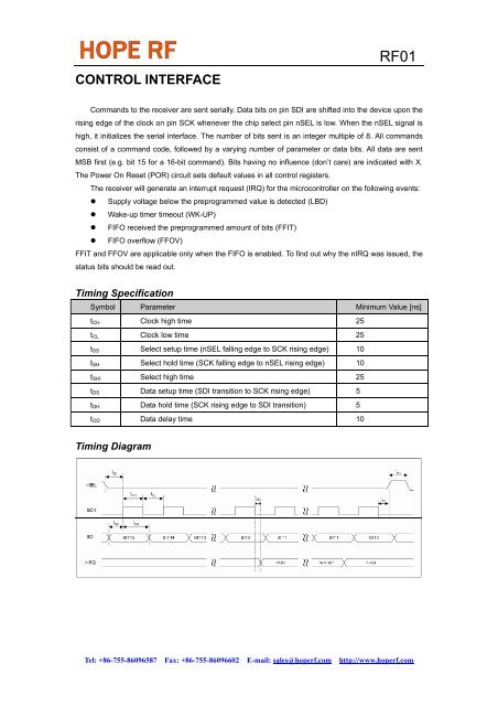
CONTROL INTERFACE<strong>RF01</strong>Commands to the receiver are sent serially. Data bits on pin SDI are shifted into the device upon therising edge of the clock on pin SCK whenever the chip select pin nSEL is low. When the nSEL signal ishigh, it initializes the serial interface. The number of bits sent is an integer multiple of 8. All commandsconsist of a command code, followed by a varying number of parameter or data bits. All data are sentMSB first (e.g. bit 15 for a 16-bit command). Bits having no influence (don’t care) are indicated with X.The Power On Reset (POR) circuit sets default values in all control registers.The receiver will generate an interrupt request (IRQ) for the microcontroller on the following events:• Supply voltage below the preprogrammed value is detected (LBD)• Wake-up timer timeout (WK-UP)• FIFO received the preprogrammed amount of bits (FFIT)• FIFO overflow (FFOV)FFIT and FFOV are applicable only when the FIFO is enabled. To find out why the nIRQ was issued, thestatus bits should be read out.Timing SpecificationSymbol Parameter Minimum Value [ns]t CH Clock high time 25t CL Clock low time 25t SS Select setup time (nSEL falling edge to SCK rising edge) 10t SH Select hold time (SCK falling edge to nSEL rising edge) 10t SHI Select high time 25t DS Data setup time (SDI transition to SCK rising edge) 5t DH Data hold time (SCK rising edge to SDI transition) 5t OD Data delay time 10Timing DiagramTel: +86-755-86096587 Fax: +86-755-86096602 E-mail: sales@hoperf.com http://www.hoperf.com