User's Manual - Crown Broadcast
User's Manual - Crown Broadcast
User's Manual - Crown Broadcast

Create successful ePaper yourself
Turn your PDF publications into a flip-book with our unique Google optimized e-Paper software.
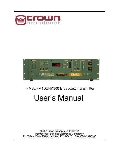
FM30/FM150/FM300 <strong>Broadcast</strong> Transmitter<strong>User's</strong> <strong>Manual</strong>©2007 <strong>Crown</strong> <strong>Broadcast</strong>, a division ofInternational Radio and Electronics Corporation25166 Leer Drive, Elkhart, Indiana, 46514-5425 U.S.A. (574) 262-8900
Revision ControlRevisionPrint DateInitial Release March 2007Important Notices©2007, <strong>Crown</strong> <strong>Broadcast</strong>, a division of International Radio and Electronics Corporation.Portions of this document were originally copyrighted by Michael P. Axman in 1994.All rights reserved. No part of this publication may be reproduced, transmitted, transcribed,stored in a retrieval system, or translated into any language in any form by any meanswithout the written permission of International Radio and Electronics, Inc.Printed in U.S.A.<strong>Crown</strong> <strong>Broadcast</strong> attempts to provide information that is accurate, complete, and useful.Should you find inadequacies in the text, please send your comments to the followingaddress:International Radio and Electronics CorporationP.O. Box 2000Elkhart, Indiana, 46515-2000 U.S.A.ii
ContentsSection 1– Getting Acquainted 1-11.1 Your Transmitter 1-21.2 Applications and Options 1-31.2.1 Stand Alone 1-41.2.2 Backup 1-41.2.3 Booster 1-41.2.4 Exciter 1-41.2.5 Translator 1-51.2.6 Satellator 1-61.2.7 Nearcasting 1-61.3 Transmitter/Exciter Specifications 1-71.4 Receiver Specifications 1-91.5 Safety Considerations 1-101.5.1 Dangers 1-101.5.2 Warnings 1-101.5.3 Cautions 1-10Section 2– Installation 2-12.1 Operating Environment 2-22.2 Power Connections 2-22.2.1 AC Line Voltage Setting 2-22.2.2 Fuses 2-52.2.3 Battery Power 2-52.3 Frequency (Channel) Selection 2-52.3.1 Modulation Compensator 2-72.4 Receiver Frequency Selection 2-72.5 RF Connections 2-102.6 Audio Input Connections 2-112.7 SCA Input Connections 2-122.8 Composite Input Connection 2-122.9 Audio Monitor Connections 2-132.10 Pre-emphasis Selection 2-132.11 Program Input Fault Time-out 2-142.12 Remote I/O Connector 2-14iii
Section 3-Operation 3-13.1 Initial Power-up Procedures 3-23.2 Power Switches 3-43.2.1 DC Breaker 3-43.2.2 Power Switch 3-43.2.3 Carrier Switch 3-43.3 Front Panel Bar-Dot Displays 3-53.3.1 Audio Processor Input 3-53.3.2 Highband and Wideband Display 3-53.3.3 Modulation Display 3-53.4 Input Gain Switches 3-63.5 Processing Control 3-63.6 Stereo-Mono Switch 3-63.7 RF Output Control 3-73.8 Digital Multimeter 3-73.9 Fault Indicators 3-8Section 4-Principals of Operation 4-14.1 Part Numbering 4-24.2 Audio Processor Circuit 4-34.3 Stereo Generator Circuit 4-44.4 RF Exciter Circuit Board 4-64.5 Metering Circuit Board 4-84.6 Motherboard 4-94.7 Display Circuit Board 4-104.8 Voltage Regulator Circuit Board 4-114.9 Power Regulator Circuit Board 4-124.10 RF Driver/Amplifier (FM30) 4-124.11 RF Driver (FM150/FM300) 4-134.12 RF Amplifier (FM150/FM300 4-134.13 Chassis 4-144.14 RF Output Filter & Reflectometer 4-144.15 Receiver Circuit Board Option 4-15iv
Section 5-Adjustments and Tests 5-15.1 Audio Processor Adjustments 5-25.1.1 Pre-Emphasis Selection 5-25.1.2 Pre-Emphasis Adjustment 5-25.2 Stereo Generator Adjustments 5-25.2.1 Separation 5-25.2.2 Composite Output 5-2Using a Modulation Monitor 5-35.2.3 19kHz Level 5-45.2.4 19kHz Phase 5-45.3 Frequency Synthesizer Adjustments 5-45.3.1 Frequency (Channel) Selection 5-45.3.2 Modulation Compensator 5-45.3.3 Frequency Measurement and Adjustment 5-45.3.4 FSK Balance Control 5-55.4 Metering Board Adjustments 5-55.4.1 Power Calibrate 5-55.4.2 Power Set 5-55.4.3 SWR Calibrate 5-55.4.4 PA Current Limit 5-65.5 Motherboard Adjustments 5-65.6 Display Modulation Calibration 5-65.7 Voltage Regulator Adjustment 5-65.8 Bias Set (RF Power Amplifier) 5-75.9 Performance Verification 5-75.9.1 Audio Proof of Performance Measurements 5-75.9.2 De-Emphasis Input Network 5-75.10 Carrier Frequency 5-85.11 Output Power 5-85.12 RF Bandwidth and RF Harmonics 5-85.13 Pilot Frequency 5-85.14 Audio Frequency Response 5-95.15 Audio Distortion 5-95.16 Modulation Percentage 5-95.17 FM and AM Noise 5-95.18 Stereo Separation 5-95.19 Crosstalk 5-95.19.1 Main Channel Into Sub 5-105.19.2 Sub Channel Into Main 5-105.20 38kHz Subcarrier Suppression 5-105.21 Additional Checks 5-10v
Section 6-Reference Drawings 6-16.1 Views 6-26.2 Board Layouts and Schematics 6-4Section 7-Service and Support 7-17.1 Service 7-27.2 24-Hour Support 7-27.3 Spare Parts 7-2Transmitter Output EfficiencyAppendix-1Glossary G-1IndexIndex-1vi
Section 1—Getting AcquaintedThis section provides a general description of the FM30, FM150, andFM300 transmitters and introduces you to safety conventions usedwithin this document. Review this material before installing or operatingthe transmitter.Getting Acquainted1-1
1.1 Your TransmitterThe FM30, FM150, and FM300 are members of a family of FM stereo broadcasttransmitters. <strong>Crown</strong> transmitters are known for their integration, ease-of-use, andreliability.The integration is most apparent in the standard transmitter configuration whichincorporates audio processing, stereo generation, and RF amplification withoutcompromised signal quality. A single <strong>Crown</strong> transmitter can replace several pieces ofequipment in a traditional system.Ease-of-use is apparent in the user-friendly front panel interface and in the installationprocedure. Simply select your operating frequency (using 5 external switches), add anaudio source, attach an antenna, and connect AC or DC power and you're ready tobroadcast. Of course, the FM series of transmitters also feature more sophisticatedinputs and monitoring connections if needed.Reliability is a <strong>Crown</strong> tradition. The first <strong>Crown</strong> transmitters were designed for rigors ofworldwide and potentially portable use. The modular design, quality components,engineering approach, and high production standards ensure stable performance.Remote control and metering of the transmitter are made possible through a built-in I/Oport. For more direct monitoring, the front panel includes a digital multimeter display andstatus indicators. Automatic control circuitry provides protection for high VSWR as wellas high current, voltage, and temperature conditions.Illustration 1-1 FM150 Stereo <strong>Broadcast</strong> TransmitterThis manual describes the FM30, FM150, and FM300 because all three transmittersshare common design factors. Specific product differences are noted throughout themanual. In physical appearance, the FM30 differs from the FM150 and FM300 in that itlacks the power amplifier and cooling fan assembly on the back panel.1-2 FM30/FM150/FM300 User’s <strong>Manual</strong>
1.2 Applications and Options<strong>Crown</strong> transmitters are designed for versatility in applications. They have been used asstand-alone and backup transmitters and in booster, translator, satellator, and nearcastapplications. The following discussion describes these applications further.Model numbers describe the configuration of the product (which has to do with its intendedpurpose) and the RF output power which you can expect.The number portion of each name represents the maximum RF output power. The FM300,for example, can generate up to 300 watts of RF output power.Suffix letters describe the configuration. The FM300T, for example, is the standard ortransmitter configuration. Except where specified, this document describes the transmitterconfiguration. In this configuration, the product includes the following components(functions):• Audio Processor/Stereo Generator• RF Exciter• Metering• Low-Pass filterIllustration 1–2 Standard (Transmitter) ConfigurationGetting Acquainted1-3
1.2.1 Stand-AloneIn the standard configuration, the FM30, FM150, and FM300 are ideal stand-alonetransmitters. When you add an audio source (monaural, L/R stereo, or composite signal),an antenna, and AC or DC power, the transmitter becomes a complete FM stereo broadcaststation, capable of serving a community.As stand-alone transmitters, <strong>Crown</strong> units often replace multiple pieces of equipment in atraditional setup (exciter, audio processor, RF amplifier).1.2.2 BackupIn the standard configuration, <strong>Crown</strong> transmitters are also used in backup applications.Should your primary transmitter become disabled, you can continue to broadcast whilerepairs take place. In addition, the FM transmitters can replace disabled portions of yourexisting system including the exciter, audio processor, or amplifier. Transfer switches oneach side of the existing and backup transmitters make the change-over possible withminimal downtime.The DC operation option of the FM30, FM150, and FM300 make them attractive backupunits for those times when AC power is lost.1.2.3 ExciterIn addition to the standard configuration, the FM30, FM150, and FM300 are available in optionalconfigurations to meet a variety of needs.An "E" suffix, as in the FM30E, for example, represents an exciter-only configuration. In thisconfiguration, the audio processor and stereo generator boards are replaced with circuitry tobypass their function. The exciter configurations are the least expensive way to get <strong>Crown</strong>quality components into your transmission system.You might consider the <strong>Crown</strong> exciter when other portions of your system are performingsatisfactorily and you want to maximize your investment in present equipment.1-4 FM30/FM150/FM300 User’s <strong>Manual</strong>
1.2.4 TranslatorA receiver configuration (FM150R, for example) replaces the audio processor/stereo generatorboard with a receiver module. This added feature makes the FM30, FM150, andFM300 ideal for translator service in terrestrial-fed networks. These networks represent apopular and effective way to increase your broadcasting coverage. Translators, acting asrepeater emitters, are necessary links in this chain of events.Traditionally, network engineers have relied on multiple steps and multiple pieces of equipmentto accomplish the task. Others have integrated the translator function (receiver andexciter) to feed an amplifier. <strong>Crown</strong>, on the other hand, starts with an integrated transmitterand adds a solid-state Receiver Module to form the ideal translator.Illustration 1–3 <strong>Crown</strong>'s Integrated TranslatorThis option enables RF in and RF out on any of <strong>Crown</strong>’s FM series of transmitters. In addition,the module supplies a composite output to the RF exciter portion of the transmitter.From here, the signal is brought to full power by the built-in power amplifier for retransmission.The Receiver Module has been specifically designed to handle SCA channel output upto 100 kHz for audio and high-speed data.FSK ID programming is built-in to ensure compliance with FCC regulations regarding theon-air identification of translators. Simply specify the call sign of the repeater station whenordering. Should you need to change the location of the translator, replacement FSK chipsare available. The Receiver Module option should be ordered at the time of initial transmitterpurchase. However, an option kit is available for field converting existing <strong>Crown</strong> units.In the translator configuration there are differences in the function of the front panel, seeSection 3 for a description.Getting Acquainted1-5
1.2.5 SatellatorOne additional option is available for all configurations—an FSK Identifier (FSK IDer). Thisadded feature enables the FM30, FM150, and FM300 to transmit its call sign or operatingfrequency in a Morse code style. This option is intended for use in satellite-fed networks.Transmitters equipped in this fashion are often known as "satellators."Connect the transmitter to your satellite receiver and the pre-programmed FSK IDer doesthe rest—shifting the frequency to comply with FCC requirements and in a manner that isunnoticeable to the listener. The FSK IDer module should be ordered at the time you orderyour transmitter, but is available separately (factory programmed for your installation).Illustration 1–4 Transmitter with FSK IDer OptionAdd the FSK IDer option to the exciter configuration for the most economical satellator (acomposite input signal is required).1.2.6 NearcastingThe output power of an FM30 transmitter can be reduced to a level that could function as anear-cast transmitter. <strong>Crown</strong> transmitters have been used in this way for language translation,for re-broadcasting the audio of sporting events within a stadium, and for specializedlocal radio. The FM30 is the only transmitter that is appropriate for this application.1-6 FM30/FM150/FM300 User’s <strong>Manual</strong>
1.3 Transmitter/Exciter SpecificationsFrequency RangeRF Power OutputFM30FM150FM300RF Output Impedance87.9 MHz–107.9 MHz (76 MHz–90 MHzoptionally available)(VSWR 1.7:1 or better)3-33 Watts adjustable15-165 Watts adjustable30-330 Watts adjustable50 OhmsFrequency Stability Meets FCC specifications from 0-50degrees CAudio Input ImpedanceAudio Input LevelPre-emphasisAudio ResponseComplete TransmitterExciter only50k Ω bridging, balanced, or 600 ΩSelectable for –10 dBm to +10 dBm for75 kHz deviation at 400 HzSelectable for 25, 50, or 75 µsec; or flatConforms to 75 µsec pre-emphasiscurve as follows:±0.30 dB (50 Hz–10 kHz)±1.0 dB (10 kHz–15 kHz)±0.25 dB (50 Hz–15 kHz)Distortion (THD + Noise)Complete TransmitterExciter onlyLess than 0.7% (at 15kHz)Less than 0.3% (50Hz-15kHz)Stereo SeparationComplete TransmitterExciter onlyCrosstalkStereo PilotBetter than –40dB (50Hz-15kHz)Better than –40dB (50Hz-15kHz)Main into Sub, better than –40dBSub into Main, better than –40dB19 kHz ±2 Hz, 9% modulationGetting Acquainted1-7
Subcarrier Suppression50dB below ±75 kHz deviationFM S/N Ratio (FM noise)Complete TransmitterExciter onlyAM S/N RatioRF BandwidthBetter than –60dBBetter than –70dBAsynchronous and synchronous noisebetter than FCC requirements±120 kHz, better than –35 dB±240 kHz, better than –45 dBRF Spurious ProductsOperating EnvironmentBetter than –70dBTemperature (0°C to 50°C)Humidity (0 to 80% at 20°C)Maximum Altitude (3,000 Meters;9834 FeetAC Power 100,120, 220, or 240 volts +10%/-15%); 50/60HzFM30FM150FM300115VA297VA550VADC PowerFM30FM150FM30024-36 volts (36 volts at 3 amps requiredfor full output power)36-72 volts (48 volts @ 7 amps for fulloutput power)36-72 volts (72 volts @ 10 amps for fulloutput power)1-8 FM30/FM150/FM300 User’s <strong>Manual</strong>
Note: We set voltage and ampere requirements to assist you in designing your system. Dependingon your operating frequency, actual requirements for maximum voltage and currentreadings are 10–15% lower than stated.Regulatory Type notified FCC parts 73 and 74Meets FCC, DOC, and CCIR requirementsDimensionsWeightFM30FM150FM30013.5 x 41.9 x 44.5 cm5.25 x 16.5 x 17.5 inches10.5 kg (23 lbs)13.6 kg (30 lbs) shipping weight11.4 kg (25 lbs)14.5 kg (32 lbs) shipping weight16.8 kg (37 lbs)20.0 kg (44 lbs) shipping weightGetting Acquainted1-9
1.4 Receiver SpecificationsMonaural Sensitivity (demodulated, de-emphasized)3.5 µ V for signal-to-noise > 50 dBStereo Sensitivity (19–kHz pilot frequency added)31 µ V for signal-to-noise > 50 dBConnectorStandard type N, 50 ΩShipping Weight1 lb1.5 Safety Considerations<strong>Crown</strong> <strong>Broadcast</strong> assumes the responsibility for providing you with a safe product andsafety guidelines during its use. “Safety” means protection to all individuals who install,operate, and service the transmitter as well as protection of the transmitter itself. Topromote safety, we use standard hazard alert labeling on the product and in this manual.Follow the associated guidelines to avoid potential hazard.1.5.1 DangersDANGER represents the most severe hazard alert. Extreme bodily harm or death will occurif DANGER guidelines are not followed.1.5.2 WarningsWARNING represents hazards which could result in severe injury or death.1.5.3 CautionsCAUTION indicates potential personal injury, or equipment or property damage if the associatedguidelines are not followed. Particular cautions in this text also indicate unauthorizedradio-frequency operation.Illustration 1–5 Sample Hazard Alert1-10 FM30/FM150/FM300 User’s <strong>Manual</strong>
Section 2—InstallationThis section provides important guidelines for installing your transmitter.Review this information carefully for proper installation.Installation2-1
2.1 Operating EnvironmentYou can install the FM transmitter in a standard component rack or on a suitable surfacesuch as a bench or desk. In any case, the area should be as clean and well ventilated aspossible. Always allow for at least 2 cm of clearance under the unit for ventilation. If you setthe transmitter on a flat surface, install spacers on the bottom cover plate. If you install thetransmitter in a rack, provide adequate clearance above and below. Do not locate the transmitterdirectly above a hot piece of equipment.2.2 Power ConnectionsThe FM30, FM150, and FM300 operate on 100, 120, 220, or 240 volts AC (50 or 60 Hz; singlephase). Each transmitter can operate on DC power as well (28 volts for the FM30, 48volts for the FM150, and 72 volts for the FM300). The transmitter can operate on fewer voltsDC, but with reduced RF output power (see section 1.3). In addition, the transmitter isolatesthe AC and DC sources; both can be connected at the same time to provide battery backupin the event of an AC power failure.2.2.1 AC Line Voltage SettingTo change the voltage setting, follow these steps:1. Disconnect the power cord if it is attached.2. Open the cover of the power connector assembly using a small, flat blade screwdriver. See Illustration 2–1.3. Insert the screwdriver into the voltage selection slot and remove the drum from the assembly.4. Rotate the drum to select the desired voltage. See Illustration 2–2.5. Replace the drum and cover and check to see that the correct voltage appears in theconnector window.6. Connect the AC power cord.2-2 FM30/FM150/FM300 User’s <strong>Manual</strong>
Illustration 2–1 Removing the Power Connector CoverIllustration 2–2 Selecting an AC Line VoltageInstallation2-3
2.2.2 FusesThe fuse holders are located in the power connector assembly just below the voltage selector.Illustration 2–3 Fuse HolderFor 100 to 120 VAC operation, use the fuse installed at the factory. For 220 to 240 VAC operation,use the slow-blow fuse located in a hardware kit within the transmitter packaging.Consult the following table:Transmitter Input Power FuseFM30 100–120 V 3 A220–240 V 1.5 AFM150 100–120 V 6.3 A220–240 V 4 AFM300 100–120 V 12.5 A220–240 V 6.3 AIllustration 2–4 Fuse Reference Table2-4 FM30/FM150/FM300 User’s <strong>Manual</strong>
2.2.3 Battery PowerYour transmitter can operate on a DC power source (such as 4 or 5, 12–volt deep cycle batteriesconnected in series). The FM30 requires 28 volts DC for full output power, while theFM150 requires 48 volts, and FM300 requires 72 volts for full output power. Connect thebatteries to the red (+) and black (–) battery input binding posts on the rear panel.2–5 Illustration DC Input Terminals2.3 Frequency (Channel) SelectionYour transmitter is capable of operating between 87.9 and 107.9 MHz in the FM band. Thetransmitter can also operate between 76 and 90 MHz by shorting pins 9 and 10 of J20 onthe motherboard. (See illustration 2-6)To adjust the operating frequency, follow these steps:1. Locate the frequency selector switches on the front panel which will be used to changethe setting. See Illustrations 2–6 and 2–7.Installation2-5
2. Use small flat blade screwdriver or another suitable device to rotate the switches to thedesired setting. (The selected number will appear directly above the white indicator doton each switch.) See examples of selected frequencies in the illustration below.3. To change the operating band from 87.9-107.9MHz to 76-90MHz or vice versa, or to adjustthe modulation compensation pot, remove the top cover to gain access to these features.See illustrations 2-6 and 2-10.Illustration 2–6 Top Cover RemovedMegahertz .1.01Illustration 2–7 Transmitter Front Panel (Frequency Selector Switches)= 88.10 MHzIllustration 2–8 Two Sample Frequency Selections= 107.90 MHz2-6 FM30/FM150/FM300 User’s <strong>Manual</strong>
2.3.1 Modulation CompensatorThe Modulation trim-potentiometer (see illustration 2–10) compensates for slight variationsin deviation sensitivity with frequency. Set the trim-pot dial according to the following graph:Frequency of Operation (MHz)Modulation Compensation Pot Setting108 0106 10104 15102 25100 3598 4097.1 4596 5594 6092 7090 7588 8086 8084 8082.4 7082 6580 5578 3076 0Illustration 2–9 Modulation Compensator SettingsThese compensator settings are approximate. Each mark on the potentiometer representsabout 1.8% modulation compensation.Illustration 2–10 Modulation Compensator PotInstallation2-7
2.4 Receiver Frequency SelectionIf you have a transmitter equipped with the receiver option, you will need to set the receivingor incoming frequency.1. With the top cover removed, locate the receiver module and the two switches (labeledSW1 and SW2).Illustration 2–11 Receiver Module Switches2. Use the adjacent chart to set the switches for the desired incoming frequency.3. For frequencies in the Japan FM band, short pins 7&8 on J1 on the receiver card.4. For 75us pre-emphasis short pins 3&4 and 5&6 on J2 of the Receiver card.5. For 50us pre-emphasis short pins 1&2 and 7&8 on J2 of the Receiver card.6. After setting the frequency, replace the top cover and screws.2-8 FM30/FM150/FM300 User’s <strong>Manual</strong>
Freq. 74-90 Freq. 88-108 SW1 SW2 Freq. 74-90 Freq. 88-108 SW1 SW2MHz MHzMHz MHz74.9 87.9 0 0 78.9 91.9 1 475.0 88.0 8 0 79.0 92.0 9 475.1 88.1 0 1 79.1 92.1 1 575.2 88.2 8 1 79.2 92.2 9 575.3 88.3 0 2 79.3 92.3 1 675.4 88.4 8 2 79.4 92.4 9 675.5 88.5 0 3 79.5 92.5 1 775.6 88.6 8 3 79.6 92.6 9 775.7 88.7 0 4 79.7 92.7 1 875.8 88.8 8 4 79.8 92.8 9 875.9 88.9 0 5 79.9 92.9 1 976.0 89.0 8 5 80.0 93.0 9 976.1 89.1 0 6 80.1 93.1 1 A76.2 89.2 8 6 80.2 93.2 9 A76.3 89.3 0 7 80.3 93.3 1 B76.4 89.4 8 7 80.4 93.4 9 B76.5 89.5 0 8 80.5 93.5 1 C76.6 89.6 8 8 80.6 93.6 9 C76.7 89.7 0 9 80.7 93.7 1 D76.8 89.8 8 9 80.8 93.8 9 D76.9 89.9 0 A 80.9 93.9 1 E77.0 90.0 8 A 81.0 94.0 9 E77.1 90.1 0 B 81.1 94.1 1 F77.2 90.2 8 B 81.2 94.2 9 F77.3 90.3 0 C 81.3 94.3 2 077.4 90.4 8 C 81.4 94.4 A 077.5 90.5 0 D 81.5 94.5 2 177.6 90.6 8 D 81.6 94.6 A 177.7 90.7 0 E 81.7 94.7 2 277.8 90.8 8 E 81.8 94.8 A 277.9 90.9 0 F 81.9 94.9 2 378.0 91.0 8 F 82.0 95.0 A 378.1 91.1 1 0 82.1 95.1 2 478.2 91.2 9 0 82.2 95.2 A 478.3 91.3 1 1 82.3 95.3 2 578.4 91.4 9 1 82.4 95.4 A 578.5 91.5 1 2 82.5 95.5 2 678.6 91.6 9 2 82.6 95.6 A 678.7 91.7 1 3 82.7 95.7 2 778.8 91.8 9 3 82.8 95.8 A 7Illustration 2–12-1 Receiver Frequency Selection(Continued on next page)Installation2-9
Freq. 74-90 Freq. 88-108 SW1 SW2 Freq. 74-90 Freq. 88-108 SW1 SW2MHz MHzMHz MHz82.9 95.9 2 8 86.6 99.6 B A83.0 96.0 A 8 86.7 99.7 3 B83.1 96.1 2 9 86.8 99.8 B B83.2 96.2 A 9 86.9 99.9 3 C83.3 96.3 2 A 87.0 100.0 B C83.4 96.4 A A 87.1 100.1 3 D83.5 96.5 2 B 87.2 100.2 B D83.6 96.6 A B 87.3 100.3 3 E83.7 96.7 2 C 87.4 100.4 B E83.8 96.8 A C 87.5 100.5 3 F83.9 96.9 2 D 87.6 100.6 B F84.0 97.0 A D 87.7 100.7 4 084.1 97.1 2 E 87.8 100.8 C 084.2 97.2 A E 87.9 100.9 4 184.3 97.3 2 F 88.0 101.0 C 184.4 97.4 A F 88.1 101.1 4 284.5 97.5 3 0 88.2 101.2 C 284.6 97.6 B 0 88.3 101.3 4 384.7 97.7 3 1 88.4 101.4 C 384.8 97.8 B 1 88.5 101.5 4 484.9 97.9 3 2 88.6 101.6 C 485.0 98.0 B 2 88.7 101.7 4 585.1 98.1 3 3 88.8 101.8 C 585.2 98.2 B 3 88.9 101.9 4 685.3 98.3 3 4 89.0 102.0 C 685.4 98.4 B 4 89.1 102.1 4 785.5 98.5 3 5 89.2 102.2 C 785.6 98.6 B 5 89.3 102.3 4 885.7 98.7 3 6 89.4 102.4 C 885.8 98.8 B 6 89.5 102.5 4 985.9 98.9 3 7 89.6 102.6 C 986.0 99.0 B 7 89.7 102.7 4 A86.1 99.1 3 8 89.8 102.8 C A86.2 99.2 B 8 89.9 102.9 4 B86.3 99.3 3 9 90.0 103.0 C B86.4 99.4 B 9 X 103.1 4 C86.5 99.5 3 A X 103.2 C CIllustration 2–12-2 Receiver Frequency Selection(Continued on next page)2-10 FM30/FM150/FM300 User’s <strong>Manual</strong>
Freq. 74-90 Freq. 88-108 SW1 SW2 Freq. 74-90 Freq. 88-108 SW1 SW2MHz MHzMHz MHzX 103.3 4 D X 107.0 D FX 103.4 C D X 107.1 6 0X 103.5 4 E X 107.2 E 0X 103.6 C E X 107.3 6 1X 103.7 4 F X 107.4 E 1X 103.8 C F X 107.5 6 2X 103.9 5 0 X 107.6 E 2X 104.0 D 0 X 107.7 6 3X 104.1 5 1 X 107.8 E 3X 104.2 D 1 X 107.9 6 4X 104.3 5 2 X 108.0 E 4X 104.4 D 2X 104.5 5 3X 104.6 D 3X 104.7 5 4X 104.8 D 4X 104.9 5 5X 105.0 D 5X 105.1 5 6X 105.2 D 6X 105.3 5 7X 105.4 D 7X 105.5 5 8X 105.6 D 8X 105.7 5 9X 105.8 D 9X 105.9 5 AX 106.0 D AX 106.1 5 BX 106.2 D BX 106.3 5 CX 106.4 D CX 106.5 5 DX 106.6 D DX 106.7 5 EX 106.8 D EX 106.9 5 FIllustration 2–12-3 Receiver Frequency SelectionInstallation2-11
2.5 RF ConnectionsConnect the RF load, an antenna or the input of an external power amplifier, to the type-N,RF output connector on the rear panel. VSWR should be 1.5:1 or better.The RF monitor is intended primarily for a modulation monitor connection. Informationgained through this connection can supplement that which is available on the transmitterfront panel displays.If your transmitter is equipped with the receiver option, connect the incoming RF to the RFIN connector.Illustration 2–13 RF Connections2-12 FM30/FM150/FM300 User’s <strong>Manual</strong>
2.6 Audio Input ConnectionsAttach audio inputs to the Left and Right XLR connectors on the rear panel. (The Leftchannel audio is used on Mono.) Pin 1 of the XLR connector goes to chassis ground. Pins 2and 3 represent a balanced differential input with an impedance of about 50 kΩ . They maybe connected to balanced or unbalanced left and right program sources.The audio input cables should be shielded pairs, whether the source is balanced or unbalanced.For an unbalanced program source, one line (preferably the one connecting to pin 3)should be grounded to the shield at the source. Audio will then connect to the line going topin 2.Illustration 2–14 XLR Audio Input ConnectorsBy bringing the audio return line back to the program source, the balanced differential inputof the transmitter is used to best advantage to minimize noise. This practice is especiallyhelpful if the program lines are fairly long, but is a good practice for any distance.If the program source requires a 600 Ω termination, see the motherboard configuration charton page 4-9 for the proper configuration of the jumpers.Installation2-13
2.7 SCA Input ConnectionsYou can connect external SCA generators to the SCA In connectors (BNC-type) on the rearpanel. The inputs are intended for the 60 kHz to 99 kHz range, but a lower frequency maybe used if the transmitter is operated in Mono mode. (The 23 to 53 kHz band is used for stereotransmission.) For 7.5 kHz deviation (10% modulation), input of approximately 3.5–volts(peak-to-peak) is required.Illustration 2–15 SCA Input Connectors2.8 Composite Input ConnectionYou may feed composite stereo (or mono audio) directly to the RF exciter bypassing the internalaudio processor and stereo generator. To use the <strong>Crown</strong> transmitter as an RF Exciteronly ("E" version or when using the "T" version with composite input), it is necessary to usethe Composite Input section of the transmitter. This will feed composite stereo (or mono audio)directly to the RF exciter. In the "T" version, this will bypass the internal audio processorand stereo generator.Input sensitivity is approximately 3.5–volt P-P for 75 kHz deviation.1. Enable the Composite Input by grounding pin 14 of the Remote I/O connector(see Illustration 2–18).2. Connect the composite signal using the Composite In BNC connector.2-14 FM30/FM150/FM300 User’s <strong>Manual</strong>
Illustration 2–16 Composite In and Audio Monitor Connections2.9 Audio Monitor ConnectionsProcessed, de-emphasized samples of the left and right audio inputs to the stereo generatorare available at the Monitor jacks on the rear panel. The signals are suitable for feedinga studio monitor and for doing audio testing. De-emphasis is normally set for 75 µsec; set to50 µsec by moving jumpers, HD201 and HD202, on the Audio Processor/Stereo Generatorboard.2.10 Pre-emphasis SelectionSelect the pre-emphasis curve (75 µsec, 50 µsec, 25 µsec, or Flat) by jumpering the appropriatepins of header HD1 on the Audio Processor/Stereo Generator board. If you changethe pre-emphasis, change the de-emphasis jumpers HD201 and HD202 on the Audio Processor/StereoGenerator board to match.Installation2-15
2.11 Program Input Fault Time-outYou can enable an automatic turn-off of the carrier in the event of program failure. To enablethis option, see illustration 2-18 on page 2-16. The time between program failure andcarrier turn-off is set by a jumper (JP1) on the voltage regulator board (see page 6–14 forboard location). Jumper pins 1 and 2 (the two pins closest to the edge of the board) for adelay of approximately 30 seconds; pins 3 and 4 for a 2–minute delay; pins 5 and 6 for a 4–minute delay, and pins 7 and 8 for an 8– minute delay.2.12 Remote I/O ConnectorRemote control and remote metering of the transmitter is made possible through a 25–pin,D-sub connector on the rear panel. (No connections are required for normal operation.)Illustration 2–17 Remote I/O ConnectorIllustration 2–18 Remote I/O Connector (DB-25 Female)2-16 FM30/FM150/FM300 User’s <strong>Manual</strong>
Pin Number Function1. Ground2. FMV Control3. Composite Out (sample of stereo generator output)4. FSK In (Normally high; pull low to shift carrier frequency approximately7.5 KHz. Connect to open collector or relay contactsof user-supplied FSK keyer.)5. /Auto Carrier Off (Pull low to enable automatic turnoff of carrierwith program failure.)6. Meter Battery (Unregulated DC voltage; 5 VDC=50 VDC)7. Meter RF Watts (1 VDC = 100 Watts)8. Meter PA Volts (5 VDC = 50VDC)9. Remote Raise (A momentary switch, holding this pin low will slowly raise the RF output)10. Remote Lower (A momentary switch, holding this pin low will slowly lower the RF output)11. Remote SWR (A buffered metering output with a calculated reading of standing wave ratio inVDC.)12. External ALC Control13. No Connection14. /Ext. Enable (Pull low to disable the internal stereo generator and enable External CompositeInput.)15. 38 KHz Out (From stereo generator for power supply synchronization. For transmitterequipped with receiver option, this pin becomes the right audio output for an 8-ohm monitor speaker. 38 KHz is disabled.)16. ALC17. /Carrier Off ( Pull low to turn carrier off)18. Fault Summary ( line goes high if any fault light is activated.)19. Meter PA Temperature (5 VDC=100 degrees C.)20. Meter PA Current (1VDC=10 DC Amperes.)21. Front Panel Voltmeter Input.22. No Connection.23. RDS RX24. RDS TX25. GroundInstallation2-17
Notes:2-18 FM30/FM150/FM300 User’s <strong>Manual</strong>
Section 3—OperationThis section provides general operating parameters of your transmitterand a detailed description of its front panel display.Operation3-1
3.1 Initial Power-up ProceduresThese steps summarize the operating procedures you should use for the initial operation ofthe transmitter. More detailed information follows.1. Turn on the DC breaker.2. Turn on the main power switch.Illustration 3–1 DC BreakerMain PowerSwitchIllustration 3–2 Front Panel Power Switch3-2 FM30/FM150/FM300 User’s <strong>Manual</strong>
3. Verify the following:A. The bottom cooling fan runs continuously.B. The Lock Fault indicator flashes for approximately 5 seconds, then goes off.4. Set the Input Gain switches for mid-scale wideband gain reduction on an averageprogram level (see section 3.4).5. Set the Processing control (see section 3.5; normal setting is “50”).6. Set the Stereo-Mono switch to Stereo (see section 3.6).7. Turn on the Carrier switch.8. Check the following parameters on the front panel multimeter:A. RF Power should be 29–33 watts for the FM30, 145–165 watts for the FM150, and300–330 watts for the FM300.B. SWR should be less than 1.1. (A reading greater than 1.25 indicates an antennamismatch.C. ALC should be between 4.00 and 6.00 volts.D. PA DC Volts should be 26–30 volts for the FM30, 25–35 volts for the FM150, and37–52 volts for the FM300. (Varies with antenna match, power, and frequency.)E. PA DC Amperes should be 1.5–2.5 amps for the FM30, 5.5–7.5 amps for theFM150, and 7.0–9.0 amps for the FM300. (Varies with antenna match, power, andfrequency.)F. PA Temperature should initially read 20–35 degrees C (room temperature). Afterone hour the reading should be 35–50 degrees C.G. Supply DC Volts should display a typical reading of 45 V with the carrier on and 50 Vwith the carrier off for both the FM30 and FM150 products. For the FM300, thereadings should be 65 V with the carrier on and 75 V with carrier off.H. Voltmeter should be reading 0.0.The remainder of this section describes the functions of the front panel indicatorsand switches.Operation3-3
3.2 Power Switches3.2.1 DC BreakerThe DC breaker, on the rear panel, must be on (up) for transmitter operation, even whenusing AC power. Electrically, the DC breaker is located immediately after diodes which isolatethe DC and AC power supplies.3.2.2 Power SwitchThe main on/off power switch controls both the 120/240 VAC and the DC battery power input.3.2.3 Carrier SwitchThis switch controls power to the RF amplifiers and supplies a logic high to the voltageregulator board, which enables the supply for the RF driver. In addition, the Carrier Switchcontrols the operating voltage needed by the switching power regulator.A "Lock Fault" or a low pin 17 (/Carrier Off) on the Remote I/O connector will hold the carrieroff. (See section 2.12.)Carrier SwitchIllustration 3–3 Front Panel Carrier Switch3-4 FM50/FM150/FM300 User’s <strong>Manual</strong>
3.3 Front Panel Bar-Dot DisplaysBar-dot LEDs show audio input levels, wideband and highband audio gain control, andmodulation percentage. Resolution for the gain control and modulation displays is increasedover a conventional bar-graph display using dither enhancement which modulates thebrightness of the LED to give the effect of a fade from dot to dot. (See section 4.7.)3.3.1 Audio Processor InputTwo vertical, moving-dot displays for the left and right channels indicate the relative audiolevels, in 3 dB steps, at the input of the audio processor. Under normal operating conditions,the left and right Audio Processor indicators will be active, indicating the relative audio inputlevel after the Input Gain switches. During program pauses, the red Low LED will light.The translator configuration shows relative audio levels from the included receiver.3.3.2 Highband and Wideband DisplayDuring audio processing, the moving-dot displays indicate the amount of gain control forbroadband (Wide) and pre-emphasized (High) audio.As long as program material causes activity of the Wideband green indicators, determinedby the program source level and Input Gain switches, the transmitter will be fully modulated.(See section 3.4.)The Wideband indicator shows short-term “syllabic-rate” expansion and gain reductionaround a long-term (several seconds) average gain set. In the translator configuration, theWideband indicator also shows relative RF signal strength.Program material and the setting of the Processing control determine the magnitude of theshort-term expansion and compression (the rapid left and right movement of the greenlight).High-frequency program content affects the activity of the Highband indicator. With 75–µsecpre-emphasis, Highband processing begins at about 2 kHz and increases as the audio frequencyincreases. Some programs, especially speech, may show no activity while somemusic programs may show a great deal of activity.3.3.3 Modulation DisplayA 10–segment, vertical peak-and-hold, bar graph displays the peak modulation percentage.A reading of “100” coincides with 75 kHz deviation. The display holds briefly (about 0.1 seconds)after the peak. The “Pilot” indicator illuminates when the transmitter is in the stereomode.To verify the actual (or more precise) modulation percentage, connect a certified modulationmonitor to the RF monitor jack on the rear panel.Operation3-5
3.4 Input Gain SwitchesThe “+6 dB” and “+12 dB” slide switches set audio input sensitivity according to thefollowing table.Normal InputSensitivity+6dBSwitches+12dB+10dBm Down Down+4dBm Up Down-2dBm Down Up-8dBm Up UpIllustration 3–4 Input Gain SwitchesFind, experimentally, the combination of Input Gain switch settings that will bring theWideband gain-reduction indicator to mid scale for “normal” level program material. Theaudio processor will accommodate a fairly wide range of input levels with no degradationof audio quality.3.5 Processing ControlTwo factors contribute to the setting of the Processing control: program material andpersonal taste. For most program material, a setting in the range of 40 to 70 provides goodprogram density. For the classical music purist, who might prefer preservation of musicdynamics over density, 10 to 40 is a good range. The audio will be heavily processed inthe 70 to 100 range.If the program source is already well processed, as might be the case with a satellite feed,set the Processing to “0” or “10”.3.6 Stereo-Mono SwitchThe Stereo-Mono slide switch selects the transmission mode. In Mono, feed audio only tothe left channel. Although right-channel audio will not be heard as audio modulation, it willaffect the audio processing.3-6 FM30/FM150/FM300 User’s <strong>Manual</strong>
3.7 RF Output ControlSet this control for the desired output power level. Preferably, set the power with an externalRF wattmeter connected in the coaxial line to the antenna. You may also use the RF powerreading on the digital multimeter.The control sets the RF output voltage. Actual RF output power varies as the approximatesquare of the relative setting of the control. For example, a setting of “50” is approximately1/4 full power.3.8 Digital MultimeterThe four-digit numeric display in the center of the front panel provides information on transmitteroperation. Use the “Up” and “down” push-buttons to select one of the following parameters.A green LED indicates the one selected.Illustration 3–5 Digital MultimeterRF Power—Actually reads RF voltage squared, so the accuracy can be affected by VSWR(RF voltage-to-current ratio). See section 5.4 for calibration. Requires calibration with theRF reflectometer being used.SWR—Direct reading of the antenna standing-wave ratio (the ratio of the desired load impedance,50 ohms, to actual load).ALC—DC gain control bias used to regulate PA supply voltage. With the PA power supplyat full output voltage, ALC will read about 6.0 volts. When the RF output is being regulatedby the RF power control circuit, this voltage will be reduced, typically reading 4 to 5.5 volts.The ALC voltage will be reduced during PA DC overcurrent, SWR, or LOCK fault conditions.Operation3-7
PA DC Volts—Supply voltage of the RF power amplifier.PA DC Amps—Transistor drain current for the RF power amplifier.PA DC Temperature—Temperature of the RF power amplifier heatsink in degrees C.Supply DC Volts—Unregulated DC voltage at the input of the voltage regulators. For batteryoperation, this reading is the battery voltage minus a diode drop.Voltmeter—Reads the voltage at a test point located on the front edge of the motherboard.A test lead connected to this point can be used for making voltage measurements in thetransmitter. The test point is intended as a servicing aid; an alternative to an external testmeter. Remember that the accuracy is only as good as the reference voltage used by themetering circuit. Servicing a fault affected by the reference affects the Voltmeter reading.The metering scale is 0 to 199.9 volts.In the translator configuration, you can read a relative indication of RF signal strength numericallyin the Voltmeter setting.3.9 Fault IndicatorsFaults are indicated by a blinking red light as follows:SWR—Load VSWR exceeds 1.5:1. ALC voltage is reduced to limit the reflected RF power.Lock—Frequency synthesizer phase-lock loop is unlocked. This indicator normally blinks forabout five seconds at power turn-on. Whenever this light is blinking, supply voltages will beinhibited for the RF driver stage as well as for the RF power amplifier.Input—The automatic carrier-off circuit is enabled (see sections 2.11 and 2.12) and the absenceof a program input signal has exceeded the preset time. (The circuit treats white orpink noise as an absence of a program.)PA DC—Power supply current for the RF power output amplifier is at the preset limit. ALCvoltage has been reduced, reducing the PA supply voltage to hold supply current to the presetlimit.PA Temp—PA heatsink temperature has reached 50° C (122° F) for the FM30 and 80° C(176° F) for the FM150 and FM300.At about 55° C (131°F) for the FM30 or 82°C (180° F) for the FM150 and FM300, ALC voltagebegins to decrease, reducing the PA supply voltage to prevent a further increase intemperature. By 60° C (140° F) for the FM50 and 85° C (185° F) for the FM150 and FM300,the PA will be fully cut off. The heatsink fan (models FM150°and FM300 only) is proportionallycontrolled to hold the heatsink at 35 C (95° F). Above this temperature, the fan runs atfull speed.3-8 FM30/FM150/FM300 User’s <strong>Manual</strong>
Section 4—Principles of OperationThis section discusses the circuit principles upon which the transmitterfunctions. This information is not needed for day-to-day operation of thetransmitter but may be useful for advanced users and service personnel.Principles of Operation4-1
4.1 Part NumberingAs this section refers to individual components, you should be familiar with the part numberingscheme used.The circuit boards and component placement drawings use designators such as “R1”, “R2”,and “C1.” These same designators are used throughout the transmitter on several differentcircuit boards and component placement drawings. When referencing a particular componentit is necessary to also reference the circuit board that it is associated with.4-2 FM50/FM150/FM300 User’s <strong>Manual</strong>
4.2 Audio Processor/Stereo Generator Circuit BoardThe audio board provides the control functions of audio processing-compression, limiting,and expansion, as well as stereo phase-error detection, pre-emphasis and generation of thecomposite stereo signal.Illustration 6-4 and accompanying schematic may be useful to you during this discussion.The overall schematic for the audio board is divided into two sheets; one each for the processorand stereo generator sections of the board.Reference numbers are for the left channel. Where there is a right-channel counterpart, referencenumber are in parenthesis.Illustration 4–1 Audio Processor/Stereo Generator Board4.2.1 Audio Processor SectionAudio input from the XLR connector on the rear panel of the transmitter goes to instrumentamplifier, U2 (U8). Two-bit binary data on the +6 dB and +12 dB control lines sets the gainof U2 (U8) to one of four levels in 6-dB steps. Gain of U2 is determined by R5, R6, or R7(R45, R46, or R47) as selected by analog switch U1.U3 (U9) is a THAT2180 voltage-controlled amplifier with a control-voltage-to-gain constantof 6.1 mV/dB. The 2180 is a current-in/current-out device, so signal voltages at the inputand output will be zero. R11 converts the audio voltage at the output of U2 (U8) to current atthe input of U3 (U9). U3 (U9) output current is converted to audio voltage by U4A (U10A).U4B (U10B) is a unity-gain inverter. When the positive peaks at the output of U4A (U10A) orU4B (U10B) exceeds the gain-reduction threshold, U15 generates a 0.25 Volts-per-dB DCcontrol bias, producing wide-band gain reduction for U3 (U9). The dB-linear allows a frontpaneldisplay of gain control on a linear scale with even distribution of dB.Principles of Operation4-3
Q1 (Q2) is a recover/expansion gate with a threshold about 18 dB below the normal programlevel. The amount of short-term expansion and time for gain recovery is controlled bythe PROCESSING control, located on the front panel display board. (See section 3.5.)Audio components above 15,200 Hz are greatly attenuated by eighth-order switchedcapacitorelliptical filter, U5 (U11). The filter cut-off frequency is determined by a 1.52-MHzclock (100 x 15,200 Hz) signal from the stereo generator section of the board. The broadbandsignal level at the output of U5 (U11) is about 5 dB below that required for full modulation.(With normal program material, the 5 dB of headroom will be filled with preemphasizedaudio.)Pre-emphasis in microseconds is the product of the capacitance of C7 (C17), multiplied bythe current-gain of U6 (U12), times the value of R22 (R62). (For description of the deviceused for U6 (12), see explanation for U3 (U9) above.) For a 75 micro-seconds preemphasis,the gain of U6 (U12) will be about 1.11.Selection of the pre-emphasis curve (75 µS, 50 µS, or Flat) is made by moving the jumperon HD1 to the pins designated on the board. Fine adjustment of the pre-emphasis is madewith R23 (R63). (See section 5.1.)For high-band processing, the peak output of U7A (U13A) and U7B (U13B) is detected andgain-reduction bias is generated, as with the broadband processor. The high-band processing,however, shifts the pre-emphasis curve rather than affecting overall gain. Peak audiovoltages are compared to plus and minus 5-volt reference voltages at the outputs of U19Aand U19B. This same reference voltage is used in the stereo generator section.A stereo phasing error occurs when left and right inputs are of equal amplitude but oppositepolarity. The most common cause is incorrect wiring of a left or right balanced audio linesomewhere in the program chain-sometimes at the source of a recording. When this happens,all the audio is in the left-minus-right stereo subcarrier-none in the left-plus-right baseband.The error can go unnoticed by one listening on a stereo receiver, but the audio maydisappear on a mono receiver. In normal programming there may be short-term polarity reversalsof left versus right, either incidental or-for effect-intentional. A phase error of severalseconds duration is processed by U14A and U14B and interpreted as a real error. During aphasing error the right-channel level is gradually reduced by 6 dB. For a listener to a stereoradio, the right-channel volume will be lower, while on a mono receiver there will be a reductionof volume.NORMAL/TEST switch. In the TEST position, the stage gains are set to a fixed level. Seesection 6.24.2.2 Stereo Generator SectionComposite stereo signal is generated from left and right-channel audio inputs. This sectionalso has the amplifier (U201) for an optional external composite input and provision for insertionof SCA signal(s).4-4 FM30/FM150/FM300 User’s <strong>Manual</strong>
Processed, pre-emphasized left and right audio is passed through third-order lowpass filterscomprised of U202A (203A) and associated circuitry. The filters decrease the level of audioproducts below 30 Hz. This low-frequency roll off is necessary to prevent disturbance to thephase-lock loop in the RF frequency synthesizer by extremely low-frequency audio components.(See caution at section 2.8.)U204 is a precision, four-quadrant, analog multiplier. The output of U204 is the product of38 kHz applied to the Y input and the difference of left and right audio (L-R signal) appliedto the X input. The resulting output is a double sideband, suppressed carrier/the L-R subcarrier.Spectral purity of the stereo subcarrier is dependant on a pure 38-kHz sinewave at the multiplierinput.U207A and Y201 comprise a 7.6-MHz crystal oscillator from which the 19 and 38-kHz subcarriersare digitally synthesized. U207F is a buffer. The 7.6 MHz is divided by 5 in U208Ato provide 1.52 Mhz, used by switched-capacitor filters U5 and U11 in the audio section.3.8 MHz, 1.9 MHz, and 304 kHz are also derived from dividers in U208. Exclusive-ORgates, U210C and U210D, provide a stepped approximation of a 38-kHz sine wave. Withthe resistor ratios used, the synthesized sine wave has very little harmonic energy belowthe 7th harmonic. U210A and B generate the 19-kHz pilot subcarrier. U211 is a dualswitched-capacitor filter, configured as second-order, low-pass filters, each one with a Q of5. The 38 and 19-kHz outputs of pins 1 and 20, respectively, are fairly pure sine waves.Harmonic distortion products are better than 66 dB down-with a THD of less than 0.05%.SEPARATION control R244 sets the 38-kHz level at the Y input of U204.Resistor matrix R219, R220, R221, and R223 sum the L+R audio with the L-R subcarrier toproduce a current at the junction of R221 and R223 that will be converted to composite stereo(less pilot) at the output of summing amplifier U206A. SCA signal is also injected at theinput of U206A. 19-kHz pilot is combined with composite stereo in summing amplifierU206B.Analog switch U205, at the input of U206A, provides switching of left and right audio for stereoand mono modes. In the mono mode, right channel audio is disabled, and the left channelaudio is increased from 45% modulation to 100%.MON L and MON R outputs go to the AF Monitor jacks on the rear panel. R209+R210(R214+R215) and C207 (C210) is a de-emphasis network. Processed, de-emphasizedsamples of the left and right audio are used for a studio monitor and for audio testing.Jumpers at HD201 (HD202) allow selection of 50-µsec or 75-µsec de-emphasis.VR212A and B supply +7 volts and -7 volts, respectively. A 5-volt reference from the audioprocessor section supplies the subcarrier generators.For an explanation of on-board adjustments see section 5.2.Principles of Operation4-5
4.3 RF Exciter CircuitThis circuit is also known as the Frequency Synthesizer. The Frequency Synthesizer part ofthe motherboard is no longer a separate module as was the case on older transmitters.Theentire component side of the motherboard is a ground plane. Frequency selector switcheslocated on the front panel of the transmitter establish the operating frequency. The VCO(voltage-controlled oscillator) circuitry is inside an aluminum case.Illustration 6-6 and accompanying schematics can be used as reference in thisdiscussion.VCO1 operates at the synthesizer output frequency of 87 MHz to 108 MHz.The frequency is controlled by a voltage applied to pin 8 of the VCO.A sample of the RF comes from A2 and is fed to the PLL chip U13.U13 is a phase-locked-loop frequency synthesizer IC. The 10.24 MHz from thecrystal oscillator is divided to 10 kHz. Internal programmable dividers divide the87 - 108 MHz RF to 10 kHz. Differences between the two signals produce error signals atpins 7 and 8 of U14.Exciter SectionIllustration 4–2 Motherboard (Exciter Section)Frequency selector switches are read by shift registers U17 and U18. Data from the shiftregisters is read by U16 which then programs the PLL (Phase Lock Loop) IC U13.U14B is a differential amplifier and filter for the error signal. Audio that is out of phase withthat appearing on the error voltage is introduced by U14A., allowing for greater loop bandwidthwith less degradation of the low frequency audio response.Lock and unlock status signals are available at the outputs of U15E and U15F respectively.Modulation is introduced to the VCO though R72 and R122.4-6 FM30/FM150/FM300 User’s <strong>Manual</strong>
4.5 Metering CircuitThe ALC and metering circuitry is on the motherboard (see Illustration 6–6). This circuitprocesses information for the RF and DC metering, and produces ALC (RF level-control)bias. It also provides reference and input voltages for the digital panel meter, voltages forremote metering, fan control, and drive for the front-panel fault indicators.Illustration 6–6 and accompanying schematics complement this discussion.PA voltage and current come from a metering shunt on the power regulator board. The PAIinput is a current proportional to PA current; R153 converts the current to voltage used formetering and control. A voltage divider from the PAV line is used for DC voltage metering.Metering SectionIllustration 4–3 Metering CircuitU23A, U23B, and U24A, with their respective diodes, are diode linearity correction circuits.Their DC inputs come from diode detectors in the RF reflectometer in the RF low-pass filtercompartment.U24B, U24C, are components of a DC squaring circuit. Since the DC output voltage ofU24C is proportional to RF voltage squared, it is also proportional to RF power.U22C, U22A, U20A, and U22D are level sensors for RF power, reflected RF power, PAtemperature, and external PA current, respectively. When either of these parameters exceedsthe limits, the output of U22B will be forced low, reducing the ALC (RF level control)voltage, which, in turn, reduces the PA supply voltage.The DC voltage set point for U22A (reflected RF voltage) is one-fifth that of U22C (forwardRF voltage). This ratio corresponds to an SWR of 1.5:1 [(1+.2)/(1– .2)=1.5]. The U25 invertersdrive the front panel fault indicators.Principles of Operation4-7
4.6 MotherboardThe motherboard is the large board in the upper chassis interconnecting the audio processor/stereogenerator board or the optional receiver module or the Omnia digital audio processorto the RF exciter and metering circuits. The motherboard provides the interconnectionsfor this boards, eliminating the need for a wiring harness, and provides input/output filtering.The RF exciter and Metering circuits are an integral part of the motherboard and areno longer separate boards as in past transmitter designs.Also contained on the motherboard is the +5.00 volt reference and the composite drive Opamp and its associated circuitry.The motherboard has configuration jumpers associated with different options that can beadded at the time of order or at a later time as an upgrade. The motherboard configurationchart for these jumpers can be found on the following page.ConfigurationJumpersIllustration 4–4 Configuration Jumpers4-8 FM30/FM150/FM300 User’s <strong>Manual</strong>
Motherboard Jumper Configuration Chart 4.6.1Jumper FMA “E” FMA“T”50KΩ inputFMA“T”600Ω inputFMA “R”FMA“Omnia”AnaloginputFMA“Omnia”AES inputZ1 Short Short Short Short Short OpenZ2 Short Short Short Short Short OpenZ3 Open Open Short Open Open OpenZ4 Open Open Open Open Open ShortZ5 Open Open Short Open Open OpenZ6 Open Open Open Open Open ShortZ7 Open Open Short Open Open OpenZ8 Open Open Short Open Open OpenZ9 Short Open Open Open Open OpenZ10 Short Open Open Open Open OpenZ11 Short Open Open Open Open OpenZ12 Short Open Open Open Open OpenZ13 Short Open Open Open Open OpenZ14 Short Open Open Open Open OpenZ15 Open Open Open Open Open OpenZ16 Open Open Open Open Open OpenZ17 Open Open Open Open Open OpenZ18 Open Open Open Open Open OpenZ19 Open Open Open Open Open OpenZ20 Open Open Open Open Open OpenZ21 Open Open Open Open Open OpenZ22 Open Open Open Open Open OpenZ23 Short Short Short Short Short ShortZ24 Short Short Short Short Short ShortZ25 Short Short Short Short Short ShortZ26 Short Short Short Short Short ShortZ27 Short Short Short Short Short ShortZ28 Short Short Short Short Short ShortZ29 Short Short Short Short Short ShortZ30 Short Short Short Short Short ShortZ31 Open Open Open Open Open OpenZ32 Short Open Open Open Open OpenZ33 Short Open Short Open Open OpenJMP1 Open Open Open Open Open OpenJMP2 Open Open Open Open Open OpenPrinciples of Operation4-9
4.7 Display Circuit BoardThe front-panel LEDs, the numeric display, the slide switches, and the processing and RFlevel controls are mounted on the display circuit board. To access the component side ofthe board, remove the front panel by removing 12 screws. The board contains circuits forthe digital panel meter, modulation peak detector, and LED display drivers, as well as indicatorsand switches mentioned above.Illustration 6–9 and accompanying schematic complement this discussion.Left and right audio from input stages of the audio processor board (just after the Input Gainattenuator) go to the L VU and R VU input on the display board. Peak rectifiers U1A andU1B drive the left and right Audio Input displays. The LED driver gives a 3–dB per step display.The lowest step of the display driver is not used; rather a red LOW indicator lightswhen audio is below the level of the second step. Transistors Q1 and Q2 divert current fromthe LOW LEDs when any other LED of the display is lit.Resolution of the linear displays, High Band, Wide Band, and Modulation, has been improvedusing dither enhancement. With dither, the brightness of the LED is controlled byproximity of the input voltage relative to its voltage threshold. The effect is a smooth transitionfrom step to step as input voltage is changed. U6A, U6B, and associated componentscomprise the dither generator. Dither output is a triangular wave.Composite stereo (or mono) is full-wave detected by diodes D5 and D6, U7, U13, Q3, andQ4 are components of a peak sample-and-hold circuit.Oscillator, U9F, supplies a low-frequency square wave to the Fault indicators, causing themto flash on and off.Digital multimeter inputs are selected with push buttons located to the right of the multimetermenu. Signals from the push buttons are conditioned by U9A and U9B. U10 is an up/downcounter. Binary input to U11 from U10 selects a green menu indicator light, and lights theappropriate decimal point on the numeric readout. The binary lines also go to analog dataselectors on the ALC/ metering board.Processing control, R50, is part of the audio processor. (See section 4.2.)The DPM IN and DPM REF lines are analog and reference voltage inputs to digital multimeterIC U12. They originate from analog data selectors on the ALC/ metering board.4-10 FM30/FM150/FM300 User’s <strong>Manual</strong>
4.8 Voltage Regulator Circuit BoardThe voltage regulator board is the longer of two boards mounted under the chassis towardthe front of the unit. It has switch-mode voltage regulators to provide +12, –12, and 20 volts.It also contains the program detection and automatic carrier control circuits.Illustration 6–10 and accompanying schematic complement this discussion.U3E and U3F convert a 38–kHz sine wave from the stereo generator into a synchronizationpulse. In the transmitter, synchronization is not used, thus D9 is omitted.U4 and U5 form a 20–volt switching regulator running at about 35 kHz. U4 is used as apulse-width modulator; U5 is a high-side driver for MOSFET switch Q1. Supply voltage forthe two IC’s (approximately 15.5 volts) comes from linear regulator DZ2/Q5. Bootstrap voltage,provided by D10 and C14, allows the gate voltage of Q1 to swing about 15 volts abovethe source when Q1 is turned on. Current through the FET is sensed by R38 and R38A. Ifthe voltage between pin 5 and 6 of U05 exceeds 0.23 volts on a current fault, drive to Q1 isturned off. Turn-off happens cycle by cycle. The speed of the turn-off is set by C13.U6 is a switching regulator for both +12 volts and –12 volts. It runs at about 52 kHz. Energyfor –12 volts is taken from inductor L2 during the off portion of the switching cycle. The –12volts tracks the +12 volts within a few tenths of a volt. There will be no –12 volts until currentis drawn from the +12 volts.Q2, Q3, and Q4 form an active filter and switch, supplying DC voltage to the RF driver,when the Carrier switch is on.The program detection circuit is made up of U1 and U2. U1A and U1D and associated circuitrydiscriminate between normal program material and white noise (such as might be presentfrom a studio-transmitter link during program failure) or silence. U1A and surroundingcomponents form a band-pass filter with a Q of 3 tuned to about 5 kHz. U1D is a first-orderlow-pass filter. Red and green LEDs on the board indicate the presence or absence of programdetermined by the balance of the detected signals from the two filters. U2 and U1Cform a count-down timer. The time between a program fault and shutdown is selected byjumpering pins on header JP1. For times, see section 5.7. The times are proportional to thevalue of R21 (that is, times can be doubled by doubling the value of R21) and are listed inminutes.Principles of Operation4-11
4.9 Power Regulator Circuit BoardThe power regulator board is the shorter of two boards mounted under the chassis towardthe front of the unit. The board has the isolating diode for the battery input, the switch-modevoltage regulator for the RF power amplifier, and circuitry for PA supply current metering.Illustration 6–10 and accompanying schematic complement this discussion.Diode D4, in series with the battery input, together with the AC-supply diode bridge, providesdiode OR-ing of the AC and DC supplies.U1 and U2 form a switching regulator running at about 35 kHz. U1 is used as a pulse-widthmodulator; U2 is a high-side driver for MOSFET switch Q1. Power for the two IC’s comesfrom the 20–volt supply voltage for the RF driver (available when the Carrier switch is on).The voltage is controlled at 16 volts by zener diode DZ1. Bootstrap voltage provided by D2and C9 allows the gate voltage of Q1 to swing about 16 volts above the source when Q1 isturned on. Current through the FET is sensed by R12A and R12B. If the voltage from pin 5to 6 of U2 exceeds 0.23 volts on a current fault, drive to Q1 is turned off. This happens on acycle-by-cycle basis. The speed of the turnoff is set by C5.U3 and Q2 are used in a circuit to convert the current that flows through metering shunt,R19, into a current source at the collector of Q3. Forty milli-volts is developed across R19for each amp of supply current (.04 ohms x 1 amp). Q3 is biased by U3 to produce thesame voltage across R16. The collector current of Q3 is the same (minus base current) asthat flowing through R22 resulting in 40 microamperes per amp of shunt current. R5 on themetering board converts Q3 collector current to 0.1 volt per amp of shunt current (.04 ma X2.49 k). (See section 5.4.)4.10 RF Driver/Amplifier (FM30)The RF Driver/Amplifier assembly is mounted on a 100 mm x 100 mm plate in the underside of the chassis.Illustration 6-14 and accompanying schematic complement this discussion.The driver amplifies the approximate 20 milliwatts from the frequency synthesizer to 30watts. An MHW6342T hybrid, high-gain, wideband amplifier, operating at about 20 volts,provides about one watt of drive to a single BLF246 MOSFET amplifier. The BLF245 stageoperates from a supply voltage of 28 volts in the FM30.The circuit board has components for input and output coupling and for power supply filtering.4-12 FM30/FM150/FM300 User’s <strong>Manual</strong>
4.11 RF Driver (FM150/FM300)The RF Driver assembly is mounted on a 100 mm x 100 mm plate in the under side of thechassis.Illustration 6-14 and accompanying schematic complement this discussion.The driver amplifies the approximate 20 milliwatts from the frequency synthesizer to about 8watts to drive the RF power amplifier. An MHW6342T hybrid, high-gain, wideband amplifier,operating at about 20 volts, provides about one watt of drive to a single BLF245 MOSFETamplifier. The BLF245 stage operates from a supply voltage of approximately 20 volts.The circuit board provides for input/output coupling and for power supply filtering.4.12 RF Amplifier (FM150/FM300)The RF power amplifier assembly is mounted on back of the chassis with four screws, locatedbehind an outer cover plate. Access the connections to the module by removing thebottom cover of the unit. The RF connections to the amplifier are BNC for the input and output.Power comes into the module through a 5–pin header connection next to the RF inputjack.Illustration 6-12 and accompanying schematic complement this discussion.The amplifier is built around a ST MicroElectronics SD2942, a dual power MOSFET ratedfor 50 volts DC and a maximum power of about 350 watts. When biased for class B, thetransistor has a power gain of about 20 dB. (It is biased below class B in the transmitter.)Input transformer, T11, is made up of two printed circuit boards. The four-turn primary boardis separated from the one-turn secondary by a thin dielectric film. R12–R17 are for damping.Trim pot R11 sets the bias.Output transformer, T21, has a one-turn primary on top of the circuit board and a two-turnsecondary underneath. Inductors L21 and L22 provide power line filtering.Principles of Operation4-13
4.13 ChassisThe AC power supply components, as well as the bridge rectifier and main filter capacitor,are mounted on the chassis. Switching in the power-entry module configures the powertransformer for 100, 120, 220, or 240 VAC; see section 2.2 for switching and fuse information.A terminal strip with MOV voltage-surge suppressors and in-rush current limiters ismounted on the chassis between the power entry module and the toroidal power transformer.The main energy-storage/filter capacitor, C01, is located between the voltage and powerregulator boards. The DC voltage across the capacitor will be 45–55 volts (FM30 andFM150) or 65–70 volts (FM300) when the carrier is on.4.14 RF Output Filter & ReflectometerThe RF low-pass filter/reflectometer are located in the right-hand compartment on the top ofthe chassis. See Illustration 6–13 and accompanying schematic for more information.A ninth-order, elliptic, low-pass filter attenuates harmonics generated in the power amplifier.The capacitors for the filter are circuit board pads.The reflectometer uses printed circuit board traces for micro-strip transmission lines. Transmissionline segments (with an impedance of about 82 ohms) on either side of a 50–ohmconductor provide sample voltages representative of the square root of forward and reversepower.DC voltages, representative of forward and reflected power, go through a bulkhead filterboard to the motherboard, then to the metering board, where they are processed for powercontrol and metering and for SWR metering and protection.4-14 FM30/FM150/FM300 User’s <strong>Manual</strong>
4.15 Receiver Circuit Board OptionThis option allows the transmitter to be used as a translator. The receiver board receivesterrestrially fed RF signal and converts it to composite audio which is then fed into the exciterboard. Microprocessor controlled phase lock loop technology ensures the received frequencywill not drift, and multiple IF stages ensure high adjacent channel rejection. Refer toillustrations 4–6, 6–16 and its schematic for the following discussion.The square shaped metal can located on the left side of the receiver board is the tunermodule. The incoming RF signal enters through the BNC connector (top left corner) and istuned through the tuner module. Input attenuation is possible with the jumper labeled “LO”“DX”, on the top left corner of the receiver board. Very strong signals can be attenuated 20dB automatically by placing the jumper on the left two pins (“LO” position). An additional 20dB attenuation is also available with the jumpers in the top left corner of the board. The frequenciesare tuned by setting switches SW1 and SW2 (upper right corner). These twoswitches are read upon power up (or by momentarily shorting J7) by the microprocessor(U4). The microprocessor then tunes the tuner module to the selected frequency. The frequencyrange is 87.9 Mhz at setting “00” to 107.9 Mhz at setting “64”. Other custom rangesare available.Located in the lower left-hand corner of the Receiver Module is a 3.5mm headphone jack.Demodulated Left and Right audio is present at this jack. A regular pair of 32 ohm stereoheadphones, such as the types used with portable audio devices, can be used to monitorthe audio on the receiver module.ReceiverModuleIllustration 4–5 Receiver ModulePrinciples of Operation4-15
When a stereo signal is present, LED 3 illuminates which indicates that left and right audiois available. Then the stereo signals go to gain stages and out to the RCA jacks on the backof the cabinet. These can be used for off-air monitoring of the audio signal. Incoming frequencycan be monitored from the frequency monitor BNC jack on the back. The stereobuffer, stereo decoder, and gain stages and have no effect on the signal that goes throughthe transmitter.The power supply is fairly straight forward. The incoming 12 volt supply goes to a 7809, 9volt regulator (VR1) which supplies all 9–volt needs on the board. The 9 volts also suppliesa 7805, 5 volt regulator (VR2) which supplies all 5–volt needs on the board. Plus and minus12 volts from the motherboard is filtered and supplies various needs on the board. Finallythere is a precision reference voltage. Two 2.5 volt reference shunts act very much like avery accurate zener diode to provide a precision 5 volt supply to the metering board.4-16 FM30/FM150/FM300 User’s <strong>Manual</strong>
Section 5—Adjustments and TestsThis section describes procedures for (1) advanced users who may beinterested in customizing or optimizing the performance of the transmitterand (2) service personnel who want to return the transmitter to operationalstatus following a maintenance procedure.Adjustments and Tests5-1
5.1 Audio Processor Adjustments5.1.1 Pre-Emphasis SelectionSelect the pre-emphasis curve (75 µsec, 50 µsec, 25 µsec, or Flat) by jumpering the appropriatepins of header HD1 on the audio processor/stereo generator board. (See section 2.9.)If you change the pre-emphasis, change the de-emphasis jumpers, HD201 and HD202 onthe audio processor/stereo generator board, to match. (See section 2.8.)5.1.2 Pre-Emphasis Fine AdjustmentTrim potentiometers, R23 and R63, (for left and right channels, respectively) provide for fineadjustment of the pre-emphasis. Set the potentiometers to bring the de-emphasized gain at10 kHz equal to that of 400 Hz. (At the proper setting, 15.0 kHz will be down about 0.7 dB.)When making these adjustments, it is important that you keep signal levels below the processorgain-control threshold.A preferred method is to use a precision de-emphasis network in front of the audio input.Then, use the non-de-emphasized (flat) output from the FM modulation monitor for measurements.5.2 Stereo Generator Adjustments5.2.1 SeparationFeed a 400–Hz sine wave into one channel for at least 70% modulation. Observe the classicsingle-channel composite stereo waveform at TP301 on the RF Exciter circuit board. Adjustthe Separation control R244 for a straight centerline.Since proper adjustment of this control coincides with best stereo separation, use an FMmonitor to make or confirm the adjustment.5-2 FM30/FM150/FM300 User’s <strong>Manual</strong>
5.2.2 Composite OutputYou can make adjustments to the composite output in the following manner:Using a Modulation Monitor1. Set the Stereo-Mono switch to Mono.2. Check that the setting of the Modulation compensation control (see illustration 2–9) onthe RF Exciter circuit , falls within the range specified for the frequency of operation.(See section 2.3.1.)3. Feed a sine wave signal of about 2.5 kHz into the left channel at a level sufficient to putthe wideband gain-reduction indicator somewhere in the middle of its range.4. Set the Composite level control to produce 90% modulation as indicated on an FMmonitor.5. Apply pink noise or program material to the audio inputs and confirm, on both Mono andStereo, that modulation peaks are between 95% and 100%.5.2.3 19–kHz LevelAdjust the 19–kHz pilot for 9% modulation as indicated on an FM modulation monitor.(The composite output should be set first, since it follows the 19–kHz Level control.)5.2.4 19–kHz Phase1. Apply a 400–Hz audio signal to the left channel for at least 70% modulation.2. Look at the composite stereo signal at TP301 on the RF Exciter circuit board with an oscilloscope,expanding the display to view the 19–kHz component on the horizontal centerline.3. Switch the audio to the right-channel input. When the 19–kHz Phase is properly adjusted,the amplitude of the 19–kHz will remain constant when switching between leftand right.4. Recheck the separation adjustment as described in section 5.2.1.5.3 Frequency Synthesizer Adjustments5.3.1 Frequency (Channel) SelectionRefer to section 2.3.Adjustments and Tests5-3
5.3.2 Modulation CompensatorRefer to section 2.3.15.3.3 Frequency Measurement and AdjustmentNext to the 10.24–MHz VCXO in the RF Exciter circuit on the motherboard, is a 50K potentiometer(R101). Use R101 to set the frequency of the 10.24–MHz VCXO while observing theoutput frequency of the synthesizer.Use one of two methods for checking frequency:1. Use an FM frequency monitor.2. Couple a frequency counter of known accuracy to the output of the synthesizer and observethe operating frequency.5.3.4 FSK Frequency Offset ControlAn FSK signal (used for automatic identification of FM repeaters) shifts the frequencies ofthe 10.24–MHz VCXO reference oscillator and the VCO.Ground pin 4 on the DB25 connector located on the back panel of the transmitter. This willshift the operating frequency. Adjust R224 for an offset of the operating frequency of about6 kHz. Un-grounding pin 4 will cause the operating frequency to return to normal.Use one of two methods for checking frequency:1. Use an FM frequency monitor.2. Couple a frequency counter of known accuracy to the output of the synthesizer and observethe operating frequency.5.4 Metering Adjustments5.4.1 Power CalibrateWhile looking at RF Power on the digital panel meter, set the Power Calibrate trim potentiometer(R215) to agree with an external RF power meter.5.4.2 Power SetWith the front panel RF Output control fully clockwise, adjust the Power Set trim pot (R55)to 10% more than the rated power (33 W for FM30, 165 W for FM150, 330 W for FM300) asindicated on an accurate external watt meter. If the authorized power is less than the maximumwatts, you may use the Power Set to limit the range of the RF Output control.5-4 FM30/FM150/FM300 User’s <strong>Manual</strong>
5.4.3 SWR CalibrateWhen the Carrier switch is off, or the RF power is less than about 5 watts, the SWR circuitautomatically switches to a calibrate-check mode. (See section 4.5 for more information.)Set the digital panel meter to read SWR. With the Carrier switch off, set the SWR CAL trimpot (R66) to read 1.03.5.4.4 PA Current LimitSince it may not be practical to increase the PA current to set the PA Current Limit control,you may use this indirect method.With the carrier turned off, look at the DC voltage at the right end of R186 in the Meteringcircuit on the motherboard. The current limit, in amperes, will be 0.35 amps higher than tentimes this voltage. For example, for a current limit of 7.35 amps, adjust the PA Current Limitcontrol for 0.7 volts at R186 ; or 0.565 volts for 6.0 amps. Set the current limit for 4 amps(FM50), 7 amps (FM150), or 9.5 amps (FM300).5.5 Motherboard ConfigurationSee section 4.6.1 for motherboard jumper configuration.5.6 Display Modulation CalibrationThe Modulation Calibrate trim pot sets the sensitivity of the front panel Modulation bar graphdisplay.This adjustment may be made only after the Output trim pot on the Audio Processor/StereoGenerator board has been set. (See section 5.2.2.)Set the Stereo-Mono switch to Mono.Feed a sine wave source of about 2.5 kHz into the left channel at a level sufficient to put thewideband gain-reduction indicator somewhere in the middle of its range.Set the Modulation Calibrate trim pot so that the “90” light on the front panel Modulation displayjust begins to light.Adjustments and Tests5-5
5.7 Voltage Regulator AdjustmentsJP1, a 10–pin header on the Voltage Regulator board, sets the time between program failureand carrier turnoff. Pins 1 and 2 are the two pins closest to the edge of the board. Thetimes are approximate. Sections 2.11, 2.12, and 4.8 contain further information.1. Short pins 1 and 2 for a 30–second delay.2. Short pins 3 and 4 for a 2–minute delay.3. Short pins 5 and 6 for a 4–minute delay.4. Short pins 7 and 8 for an 8–minute delay.You may select other times by changing the value of R21. The time is proportional to the resistance.5.8 Bias Set (RF Power Amplifier)The Bias Set trim pot is located inside the PA module on the input circuit board. Set the trimpot to its midpoint for near-optimum bias.5-6 FM30/FM150/FM300 User’s <strong>Manual</strong>
5.9 Performance VerificationMeasure the following parameters to receive a comprehensive characterization of transmitterperformance:• Carrier frequency• RF output power• RF bandwidth and RF harmonics (see section 5.12)• Pilot frequency, phase, and modulation percentage• Audio frequency response• Audio distortion• Modulation percentage• FM and AM noise• Stereo separation between left and right• Crosstalk between main channel and subcarrier• 38–kHz subcarrier suppression• In addition to the above tests, which pertain to signal quality, a complete check of theunit will include items listed in section 5.21.5.9.1 Audio Proof-of-Performance MeasurementsReferences to “100%” modulation assume 9% pilot and 91% for the remainder of the compositestereo signal.Because the audio processing threshold is at 90% modulation, it is not possible to makeaudio proof-of-performance measurements at 100% modulation through the audio processor.Instead, data is taken at a level below the audio processing threshold at 80% modulation.5.9.2 De-emphasis Input NetworkA precision de-emphasis network, connected between the test oscillator and the audio inputof the transmitter, can be very helpful when making the audio measurements. Notethat the input impedance of the transmitter or the source impedance of the test oscillatorcan affect network accuracy. With the de-emphasis network, oscillator level adjustmentsneed only accommodate gain errors, instead of the whole pre-emphasis curve.Adjustments and Tests5-7
5.10 Carrier FrequencyCarrier frequency is measured at the output frequency with a frequency monitor or suitablefrequency counter.To adjust frequency, see section 5.3.3. (FCC tolerance +/– 2000 Hz per FCC Part 73.1540and 73.1545.)5.11 Output PowerThe output power reading on the front panel display should be 90–105% of the actual value.For a more precise measurement, use a watt meter in the RF output line. See sections5.4.1 and 5.4.2 for setting power.5.12 RF Bandwidth and RF HarmonicsYou can observe RF bandwidth and spurious emissions with an RF spectrum analyzer.In the Stereo mode, feed a 15.0–kHz audio signal into one channel to provide 85% modulationas indicated on a monitor. Doing so produces 38% main, 38% stereo subcarrier, and9% pilot per FCC Part 2.1049. As an alternative, use pink noise into one channel.Using a spectrum analyzer, verify the following (per FCC 73.317):1. Emissions more than 600 kHz from the carrier are at least 43 + 10log(power, in watts)dB down (58 dB for 30 watts, 65 dB for 150 watts, 68 dB for 300 watts). The scanshould include the tenth harmonic.2. Emissions between 240 kHz and 600 kHz from the carrier are down at least 35 dB.3. Emissions between 120 kHz and 240 kHz from the carrier are down at least 25 dB.5.13 Pilot FrequencyThe pilot frequency should be within 2 Hz of 19 kHz. (FCC Part 73.322.) Using a frequencycounter, measure 1.9 MHz at pin 13 of U208 on the Audio Processor/Stereo Generatorboard. A 200–Hz error here corresponds to a 2–Hz error at 19 kHz. If the frequency is off bymore than 50 Hz, you may change the value of C213. (Changing C213 from 56 pF to 68 pFlowers the 1.9 MHz by about 35 Hz.)5.14 Audio Frequency ResponseFor the response tests, take the readings from an FM modulation monitor.Make audio frequency response measurements for left and right channels at frequencies of50 Hz, 100 Hz, 400 Hz, 1 kHz, 5 kHz, 10 kHz, and 15 kHz. See sections 5.9.1 and 5.9.2.5-8 FM30/FM150/FM300 User’s <strong>Manual</strong>
5.15 Audio DistortionMake distortion measurements from the de-emphasized output of an FM modulation monitor.Make audio distortion measurements for left and right channels at frequencies of 50 Hz, 100Hz, 400 Hz, 1 kHz, 5 kHz, 10 kHz, and 15 kHz. See sections 5.9.1 and 5.9.2.5.16 Modulation PercentageWhile feeding an audio signal into the left channel only, confirm that the total modulationpercentage remains constant when switching between Mono and Stereo.Measure modulation percentage with an FM modulation monitor. See section 5.2.2.19–kHz pilot modulation should be 9%.5.17 FM and AM NoiseTake noise readings from a de-emphasized output of a modulation monitor.5.18 Stereo SeparationMake left-into-right and right-into-left stereo separation measurements with an FM modulationmonitor for frequencies of 50 Hz, 100 Hz, 400 Hz, 1 kHz, 5 kHz, 10 kHz, and 15 kHz.5.19 CrosstalkFor stereo crosstalk measurements, both left and right channels are fed at the same time.For best results, there needs to be a means of correcting small imbalances in levels andphase. The balance is made at 400 Hz.5.19.1 Main Channel Into SubFeed the left and right channels in phase with audio (L+R) at 50 Hz, 100 Hz, 400 Hz, 1 kHz,5 kHz, 10 kHz, and 15 kHz at 100% modulation, while observing the stereo subcarrier (L-R)level on an FM modulation monitor.5.19.2 Sub Channel Into MainFeed the audio into the left and right channel as above, with the exception of reversing thepolarity of the audio of one channel (L-R input). Using the frequencies of 5.19.1 above, observethe main channel (L+R) level with a modulation monitor.Adjustments and Tests5-9
5.20 38–kHz Subcarrier SuppressionWith no modulation, but in the Stereo mode, the 38–kHz subcarrier, as indicated on an FMmodulation monitor, should be down at least 40 dB.5.21 Additional ChecksIn addition to the tests and adjustments mentioned in this section, the following checks ensurea complete performance appraisal of the transmitter:1. Perform a physical inspection, looking for visible damage and checking that the chassishardware and circuit boards are secure.2. Check the functionality of switches and processing control.3. Verify that all indicators function.4. Check the frequency synthesizer lock at 80 MHz and 110 MHz.5. Measure the AC line current with and without the carrier on.6. Perform a functional test of the SCA input, Monitor outputs, and the monitor and controlfunction at the 15–pin, D-sub connector.7. Test the functionality of the FSK circuit.8. Check the operation and timing of the automatic carrier-off circuitry associated with programfailure.9. Check all metering functions.10. Test ALC action with PA current overload, SWR, and PLL lock.NOTE:FCC type acceptance procedures call for testing the carrier frequency over the temperaturerange of 0–50 degrees centigrade, and at line voltages from 85% to 115% of rating. (SeeFCC Part 2.1055.)5-10 FM30/FM150/FM300 User’s <strong>Manual</strong>
Section 6—Reference DrawingsThe illustrations in this section may be useful for making adjustments,taking measurements, troubleshooting, or understanding the circuitry ofyour transmitter.Reference Drawings6-1
6.1 ViewsGainReduction/ExpansionIndicatorsDigital MultimeterFault IndicatorsCarrier SwitchMultimeter Select Modulation IndicatorsAudio ProcessorInput LevelIndicatorsInput GainSwitchesProcessing ControlFrequency SelectorSwitchesStereo/MonoSwitchIllustration 6-1 Front ViewRF OutputControlPower SwitchRF OutputReceiver Input(Optional)Composite InputAudio InputsRF Output MonitorSCA InputsAudio MonitorsAC Power InputRF Power Amplifier(FM150/300 Only)Remote I/ODC InputCircuit BreakerIllustration 6-2 Rear View6-2 FM30/FM150/FM300 User’s <strong>Manual</strong>
MeteringCircuitAudio ProcessorSectionRF Low PassFilter &ReflectometerRF ExciterCircuitStereo GeneratorSectionDC InputRF outputIllustration 6-3 Chassis Top ViewPower Amplifier(FM150/M300 Only)Voltage RegulatorPower RegulatorRF Pre-driver/AmplifierFilter CapacitorBridge RectifierAC PowerTransformerAC PowerEntryIllustration 6-4 Chassis Bottom ViewAdjustments and Tests6-3
Notes:6-4FM30/FM150/FM300 User’s <strong>Manual</strong>
6.2 Board Layout and SchematicsIllustration 6-5 Audio Processor/Stereo Generator BoardFM30/FM150/FM300 User’s <strong>Manual</strong>6-5
747455223344557766223344557766Board Layouts and Schematics1234DWG. NO.REV.5678951061112HGFL VUC1L IN21uFC2L IN11uF/+12DB/+6DBR11KC3100pFR31KC4100pFR3847K+5VGAIN R9-14---------------------------0dB OPEN+6dB 50.5K+12dB 16.8K+18dB 7.21KR3947KR249.9KR449.9K2183133+12VRG16 R11U2RG2 AD622 10.0K-12VR749.9R649.9R549.9U1120X14X 1X152X113X10Y5Y 1Y22Y43Y10A9B6INH74HC4052R4549.9R4649.9R4749.9L SAMPLE1U3THAT2180INEC+EC-SYMR122.00K R1349.9V-+12VV+-12VGNDR145.1KOUT8238 4C522pFR1549.9K-12VU4A1TL072+12VC1565R1624.9KR1724.9KU4B7TL072D11N6263D21N6263(INTO 600 ohms)dbm V-rms V-peak-10 .245 .3460 .774 1.1+10 2.45 3.4615.2 KHz LOW-PASS FILTER(8th ORDER ELLIPTICAL)R18100KQ12N5087R201KC100.1uFR19OPEN+ C2810uFTANT+7V1234567INV CVinAGNDV+AGNDCOMP1*INV ADS11N5818U5R(h I)COMP2*V-fCLKNCVoutNCLTC1064-11.52MHzDS21N5818R10510-7V141312111098TURKEY SPECIFICATIONS:Baseband:30Hz - 53KHz +/- 0.2dB.53KHz - 76KHz +/- 0.4dB.40Hz - 15KHz +/- 0.5dB40H 7 5KH 0 5% THD+C2910uFTANTC61uFC6A1uFR2310K+5V-5VR2430KR271.0KR671.0KC7.0027uFPOLY (C8687-3)R21300R281.0KR705.62KR681.0KFLAT50uS75uS1U6THAT2180INEC+EC-HD11 23 45 67 89 10SYMR2549.9HEADER 5X2R2224.9K+12VV-V+GNDR265.1K-12V+5VOUT8C833pFR2924.9K-12V2 U7A13TL072+12V8 4R3524.9K65R3624.9KU7B7TL072R37499D11N6263D11N6263+VTD51N4148D61N4148-VTLEFTC92200pFPOLYREVISION HISTORYE . C . N. REV DESCRIPTIONDATEDWNAPPROVALSCHK CMPEHGFEDCR IN2R IN1R VUL SAMPLER SAMPLEC111uFC121uFR82100KR8030KR8130KR83100KR411KC13100pFR431KC14100pFLEFT-RIGHT PHASING DETECTORRIGHT LEVEL REDUCED 6dBDURING POLARITY ERROR.D251N4148D261N6123D271N4148R4249.9KR4449.9K65C301uFD281N4148R8410M2183U14B7TL072BR GR+12VRG1U8RG2-12V238 46AD622R855.1KR86100KR8710K-12VU14A1TL072+12VR89100KR5110.0KD291N4148DL1REDSTEREOPOLARITYERRORR7910KR90100R SAMPLED211N41481U9THAT2180INEC+R522.00KR8810KEC-SYM/STEREO FAULTD221N4148V-+12VV+-12V.006V/DBR5349.9-12VU15A1TL072+12VR103240KGNDR545.1KR9149.9K8 4OUT238R9249.9KR9449.9KR9349.9K238 422pFR1549.9K-12VU10A1TL072+12VC21.047uFPOLYC20100pFD141N4148U15B 7-VTTL072R953.0K65R5624.9K65R5724.9KU10B7TL072R96ZEROD13R981N4148330KR993.3MC22100pFR1011.0KD71N6263D81N6263R10010MC231uFR603.3KR10210.0KR9710MR58100KQ22N5087PROC B(J3-18)R59OPENHEAVYPROC A(J3-16)PROC C(J3-20)LIGHTTO R50 ONDISPLAY BD.1234567U11INV C R(h I)Vin COMP2*AGND V-V+ fCLKAGND NCCOMP1* VoutINV A NCLTC1064-1141312111098HI GRC161uFC16A1uFR112100+5VR6310K-5VR6430KD16SHORT24.9KC17+12V.0027uFPOLY (C8687-3)U12THAT2180R613001INEC+EC-R62SYMR6549.9V-V+-12VGNDR665.1K0.25V/DBOUT8U16A1TL072+12V23R11349.9K8 4C1833pFR6924.9K8 4-12VU13A1TL072+12VR11449.9K-12V23 R11649.9KR11549.9KR117-VT560R7524.9K65R77499R7624.9KU13B7TL072C24.01uFPOLYC25OPEND171N4148U16B7TL072D91N6263D101N6263R11924.9KR120OPENC26100pF65+VT-VTR1183.3KR1211MR1221.0KD111N4148D121N4148R12310.0KC271uFRIGHTC192200pFPOLY+12V+12V-12V+7V-7VVDD+5V-5VVEE+VT-VTC401uFC411uFLEFTRIGHT1.52MHz+5.00V-5VGNDC421uFC431uFLEFTRIGHTCLOCK+12V-12V+7V-7V+5V-5V+VT-VTGNDC441uFC451uF+12VEDC-12V-12V+VTBAR127U184.7KREF02TEST SW118-12VNC NCC32+5.00V3272 U19A .01uFVCC2+12V Vin NC1R1281+5V+5V363NC Vout100C33 C34 C35NORMAL SIP3NE5532451uF 1uF 1uFGND TRIM+12VR12610KR129VSS10.0KC366 U19B .01uF7R130-5V5100NE5532C37 C381uF 1uF8 4+12VD231N4148+5VR1045.1KD241N414823R10510K8 4-12VU17A1NE5532+12VR10749.9KR106 6 U17B749.9K -VT5NE5532+/- 12V FOR OP-AMPS AND VCA'S.+/- 7V AT 56mA FOR LTC 1064-1 AND LMF100.+/- 5V FOR LOGIC (+5V TAKEN FROM +5.00V BUS+5.00V REFERENCE VOLTAGE. ALSO USED BY D+/- 4.4 FOR PEAK LEVEL THRESHOLD REFERENCJ11 23 45 67 89 1011 1213 1415 1617 1819 20RECEPT 10X2L IN1L IN2R IN1R IN2J31 23 45 67 89 1011 1213 1415 1617 1819 2021 2223 2425 26RECEPT 13X2+12V-12V/+6DB/+12DBL VUR VU+5.00VPROC APROC BPROC CBR GRHI GR/STEREO FAULTUNCONTROLLEDUNLESS OTHERWISE MARKED IN RED INK BY CM AS ACONTROLLED COPY, COPIES OF THESE DOCUMENTSINCLUDING ASSOCIATED ELECTRONIC REPRODUCTIONSARE FOR REFERENCE ONLY.THESE DRAWINGS AND SPECIFICATIONS ARE THEPROPERTY OF INTERNATIONAL RADIO AND ELECTRONICS CORP.AND SHALL NOT BE REPRODUCED, COPIED OR USED ASTHE BASIS FOR THE MANUFACTURE OR SALE OF APPARATUS ORDEVICES WITHOUT PERMISSION.APPROVALSDWN DW 03-15-07CHKCM DW 03-15-07PE DP 03-15-07DISTRIBUTIONKIRECCopyright (c) 2007 HCJB GlobalINTERNATIONAL RADIO AND ELECTRONICS CORP.25166 LEER DRIVE ELKHART, IN. 46514574-262-8900 WWW.IREC1.COMTITLE:AUDIO PROCESSOR/STEREO GENERATORSIZE DWG . NO .REVD201409F-SCHCBAFILENAME:SCALE : NONEPROJ NO.SHEET1 OF 21 2 3 4 5 6 7 8 9 10 11 12Schematic Diagram: Audio Processor/ Stereo Generator (Sheet 1 of 2)6-6 Adjustments and TestsFM30/150/300 User’s <strong>Manual</strong>
65581 234571234DWG. NO.REV.5678951061112HSCA INR2170C203100pFC204OPENR230HEXT IN-EXTERNAL COMPOSITEINPUTEXT IN+R2031KC202100pFR2011KR20449.9KR205OPEN1 2 83+12VU201RG1 6 R206RG2 AD622 3.9KComposite Spec. (Turkey):30Hz - 53KHz +/- 0.2 dBr53KHz - 76KHz +/- 0.4dBr0C201100pFR20249.9K-12VGGD201D202FELEFTRIGHTCLOCK+12V-12V+7V-7V+5V +5.00VLEFTRIGHT-5V -5V+VT-VTGND1.52MHzGND+12V-12V+7V-7VVDD+5V-5VVEE+VT-VTLEFTRIGHTC205.047uFPOLYC208.047uFPOLYR207150KC206.047uFPOLY R208300KR212150KC209.047uFPOLY R213300K23238 48 4-12VU202A1TL072+12V-12VU203A1TL072+12VR2094.99KR2144.99KHD201SIP3SIP3R2102.49K50 75R2152.49K1 23HD20250 75C207.01uFPOLYC210.01uFPOLY6565U202B7TL072U203B7TL072R211100LEFT 8VPP (AT 2000Hz)RIGHT 8VPP (AT 2000Hz)R216100MON LMON RR21910.0K123456R2189.09K 1%R22010.0KX1X2U0U1U2Y1U204V+ 14DDOUT1312Z1 11Z2 10REF 97 Y2 V- 8AD734+12V1N4148D2031N4148D2051N4148R2214.99KC212R222C211 120pF200K56pFR2239.09K1N4148D2041N4148D2061N41481214151115241096U2050X1X X 132X3X0Y1Y2Y3YABINH74HC4052Y 3R2241K-5V23R22643KR22512.4K8 4-12VU206A1MC34083+12VD2071N4148R2341KD2081N4148+5VR2271KCOMPOSITE OUTPUT-7V +7VC2271uFC2281uFJ20112345678910111212 HEADEREXT IN+EXT IN-SCA INCOMP OUTCOMP METERMONO/STEREO/EXT ENABLEGNDFEDCC21356pFNPOR2361KY2017.6 MHzC2145.5-18pF/EXT ENABLEMONO/STEREOR2371MU207A1 2C21533pFNPO+5VR23810KMC74HC04U207C5 6MC74HC04U207F13 12MC74HC04U208A2 1QA 31CLR154 6 1QB 1CKA1CKB 1QC1QD 774HC390U208B14 2QA 132CLR151112 10 2QB 2CKA2CKB 2QC2QD 974HC390U207B3 43.8MHz1.52MHz1.9MHz304KHz1213 CLR QA11CKA QB 10QC 9QD 8U209B74HC3931312U210D11 R24024K74HC86U210C98 R2411010K74HC86U210B56 R2424120K74HC86U210A13 R243249.9K74HC86C2160.1uFC2160.1uFCLK CLK B A 1050/100 LSH 9VD- VD+ 8VA- VA+ 7AGND SA/BS1 B S1 AINV B INV A 4HPB HPA 3BPB BPA 2LPB LPA 111SEPARATIONR2445K1213-7V+7V14R24513K151617R246 10.0K18R250 10.0K19R247 49.9K20R251 49.9KR254 used ONLY with AD633AD734 has internal 50KC2180.1uFU211LMF100C2210.1uFR2521KR2551KR25449.9KR2531KC2191000pFPOLYR2561KC2221000pFPOLYC2191000pFPOLY1234X1X2Y1Y2R25743KC223 R2581000pFPOLY1K+12VV+V-U204AOUT 7Z 6AD633JN-12VAD633 ALTERNATE TO AD 73419KHz LevelR2593KR22924K+5VR26324.9K6565U212B7TL072C22422pFR23120KU206B7MC34083R2283KR26410K+12VC224.001R232100R233100Q202MPS-A06R26510COMP OUTCOMP METER+7VR26010.0K238 4-12VU212A1TL072+12VC226.001-12VJ20212345678910111212 HEADERR26110KR26210Q201MPS-A56MON LMON RGND+5.00VSYNC OUT-7VDCBR23910KMC74HC04U209A231 4 QA CLRCKA QBQC 5QD 674HC393U207E11 10U207DMC74HC049 8MC74HC04R266OPENR2671K38KHz19KHzSYNC OUT-12V+12VDZ1ICTE-15DZ2ICTE-15J20310 98 76 54 32 1RECEPT 5X2-12V+12VBCopyright (c) 2007 HCJB GlobalAUNCONTROLLEDUNLESS OTHERWISE MARKED IN RED INK BY CM AS ACONTROLLED COPY, COPIES OF THESE DOCUMENTSINCLUDING ASSOCIATED ELECTRONIC REPRODUCTIONSARE FOR REFERENCE ONLY.Copyright 2006 Michael P. AxmanTHESE DRAWINGS AND SPECIFICATIONS ARE THEPROPERTY OF INTERNATIONAL RADIO AND ELECTRONICS CORP.AND SHALL NOT BE REPRODUCED, COPIED OR USED ASTHE BASIS FOR THE MANUFACTURE OR SALE OF APPARATUS ORDEVICES WITHOUT PERMISSION.TITLE:AUDIO PROCESSOR/STEREO GENERATORSIZE DWG . NO .REVB201409F-SCHCASCALE : NONEPROJ NO.SHEET 2 OF 21 2 3 4 5 6 7 8 9 10 11 12Schematic Diagram: Audio Processor/ Stereo Generator (Sheet 2 of 2)FM30/FM150/FM300 User’s <strong>Manual</strong>6-7
Board Layouts and SchematicsIllustration 6-6 Motherboard6-8FM30/150/300 User’s <strong>Manual</strong>Adjustments and Tests
987654321123456789321121234123DWG. NO.201207F-SCH4AREV.5678951061112HGFAN-+12VJ16J14123456HEADER 6X1 .156WR TP1ANTENNA SWRFM TP1VOLTMETERJ25123HEADER 3X1J2512345678910FANHEADER 3123+12VR2161KC55.01R150 1KR176 1KR177 1KC56.01C140.01C57.01Q3IRF541C541.0201497F-SCH-SH2.SCHFM_/LOCKALCMETER PAVMETER PAIMETER RFWMETER PATEMPMETER BATTFAULT SUMFM_/LOCKALCMETER PAVMETER PAIMETER RFWMETER PATEMPMETER BATTFAULT SUM-12V-12VGNDALC/METERING+5.00V+12V+12V+5.00V/LOCK FAULTDC SUPPLYPAIPAVEXT ALC CONTROLTEMPFANV-METERRFVRF FWDRF REVINPUT/LOCK FAULTDC SUPPLYPAIPAVEXT ALC CONTROLTEMPFANV-METERRFVRF FWDRF REVINPUTALCJ26 HEADER 5 x 2FM_/LOCK10RF_LVL+12V-12V201497F-SCH-SH3.SCHGNDFSK INLOCK/LOCKRF_LVLLOC/REMOTEFSK INLOCK/LOCKRF_LVLLOC/REMOTEALCALCRF EXCITERCOMPOSITE1COMPOSITE1RF OUT-12V-12V+12V+12V J18MCXRF OUTJ19MCXE2E3E4C261.0+12VAUDIO PROCESSOR SHUNT1234NCVinTEMPGNDU2NCNCVoutTRMREF028765C29+12V1.02 TL0721U3A3C30-12V1.065TL0727U3BC27.01R404.7KR39100C281.0Z9OPEN+5.00VREVISION HISTORYAPPROVALSE . C . N. REV DESCRIPTIONDATE DWN CHK CMA PRODUCTION RELEASE03-08-07 DW DWPEDPHGFEDCHEADER 5 x 2J13 FMV+ 1TEMP 2GND 3HEADER 3X1J29WRJ15FMJ312345678910111213141516171819201234567891011121314151617181920C66OPENC67OPENC68OPENC65.01C64.011325122411231022C62.01C60.01C58.01C59.01C63.001C61.001TEMPPAIPAVN/CN/C/LOCK FAULTNCNCNCNCNCNC+12VDC SUPPLY38KHZN/C/CARR_OFFTEMP/AUTO_CARR_OFFINPUTN/CN/CN/CN/CN/CN/CALCNC38KHZRDS TXRDS RX38KHZREM SWRREM LOWERREM PWR CNTRLWRJ28123HEADER 3X1ALCINPUTTEMPPAIPAVV+TEMPGND/LOCK FAULT/CARR_OFF/AUTO_CARR_OFFC159.001C158.001C157.001DC SUPPLYALCD11N4148ALCMETER PAVZ22 OPENZ21 OPENR28 220METER PAIZ20 OPENR27 220METER RFWZ19 OPENR26 220METER PATEMPZ18 OPENR25 220METER BATTZ17 OPENR24 220FAULT SUMZ16 OPENR23 220Z15 OPENR22 220R21 220Z23C16JUMPER .01Z24C17JUMPER .01Z25C18JUMPER .01Z26C19JUMPER .01Z27C20JUMPER .01Z28C21JUMPER .01Z29C22JUMPER .01Z30C23JUMPER .01FSK IN38KHZCOMP METER/EXT ENABLERF_LVLCOMP METERL IN1R IN1L IN2R IN2COMPOSITE1EXT IN/EXT ENABLEEXT RTNSCA INMON LMON RLPIN LLPOUT LLPIN RLPOUT R38KHZL IN1L IN2R IN1R IN2LPIN LLPOUT LLPIN RLPOUT R+5.00VSTEREO/MONCOMPOSITE1COMP METERNCNCNCJ912345678910HEADER 5 x 2J1112345678910111213141516171819NC20HEADER 10 x 2NCJ7123456789101112HEADER 12J6123456789101112HEADER 12123456789101234567891011121314151617181920123456789101112J2J1J1AUDIO PROCESSORSTEREO GENERATORJ101234567891011121314151617181920212223242526HEADER 13 x 21234567 J28910J81112 1122334455J3 6677889910 10HEADER 5 x 2J31234567891011121314151617181920212223242526NC+12V+12V-12V/+6DB/+12DBL VUR VU+5.00VPROC APROC BPROC CBR GRHI GR-12V+5.00VZ31 Z32OPEN OPENINSTALLED WHEN USINGAUDIO PROC. SHUNT CKT.COMP METERFMV CONTROLSTEREO/MON+12V-12V+12V-12V+5.00VJ121234567891011121314151617181920HEADER 10 x 2TP4+12VTP3-12VTP5+5.00VTP7GNDINPUT CONFIGURATION CHARTNON-OMNIA BOARD INPUT IMPEDENCE50 KOHMZ1, Z2 ONZ3, Z5, Z7, Z8 OFFZ4, Z6 OFF600 OHM+5VZ1, Z2 ONZ3, Z5, Z7, Z8 ONZ4, Z6 OFFTP6+5VOMNIA BOARD AES/EBU INPUTZ1, Z2 OFFZ3, Z5, Z7, Z8 OFFZ4, Z6 ONANALOG LEFT/RIGHTLEFT IN 1 LEFT IN 2FEDCBADB25_2X9218207196185174163152141-METER PAV-METER PAI-METER RFW-METER PA TEMP-METER BATT-FAULT SUM-/AUTO_CARR_OFF-/CARR OFF_FSK IN_ALC-COMPOSITE OUT38 KHZ OUT-FMV CONTROL_/EXT ENABLEREM RAISER14 220R13 100R12 390R11 390R101KR9 22010+12V38KHZHEADER 5 x 2R2221KFMV CONTROLJ24C5.01C6.001C7.001C8.001C9.01C10.01FSK INCOMPOSITE METERFMV CONTROL/EXT ENABLEJ1XLRZ5OPENZ3OPENZ6Z4R41KR21KZ1JUMPERR3300R1300OPENL IN1OPENL IN2C1220pFZ2JUMPERC2220pF231REF. FORXLR CON.R IN1C3220pFHILOGNDR IN2R81KC4220pFR5300R7300R61KZ7OPENZ8OPEN3J2OPENR151K5HD6OPENR161KR171KMON_RMON_LEXT_INEXT_RTNSCAR181KC11220pFC12220pFC13220pFC14220pFC15220pFR201KR19240SCA INEXT RTNEXT INZ13OPENZ12OPENZ14OPENZ11OPENZ10OPENR3224.9K1%R3524.9K1%R38R34 24.9K 1%C24+12V1.02 TL0721U1A3C25-12V1.0R3624.9K1%UNCONTROLLEDUNLESS OTHERWISE MARKED IN RED INK BY CM AS ACONTROLLED COPY, COPIES OF THESE DOCUMENTSINCLUDING ASSOCIATED ELECTRONIC REPRODUCTIONSARE FOR REFERENCE ONLY.STEREO GENERATOR SHUNT1KD21N41481N4148D3R31100R33100R291K R374.02K1%R306 TL07273.9K U1B5THESE DRAWINGS AND SPECIFICATIONS ARE THEPROPERTY OF INTERNATIONAL RADIO AND ELECTRONICS CORP.AND SHALL NOT BE REPRODUCED, COPIED OR USED ASTHE BASIS FOR THE MANUFACTURE OR SALE OF APPARATUS ORDEVICES WITHOUT PERMISSION.APPROVALSDWN DW 10-05-06CHKCM DW 10-05-06PE DP 10-05-06DISTRIBUTIONKFILENAME:NOTES:UNLESS OTHERWISE SPECIFIED:1. ALL RESISTORS ARE IN OHMS, 1/4W, 5% TOL.2. ALL CAPACITORS ARE IN MICROFARADS.IRECINTERNATIONAL RADIO AND ELECTRONICS CORP.25166 LEER DRIVE ELKHART, IN. 46514574-262-8900 WWW.IREC1.COMTITLE:SCH, UNIVERSAL MOTHER BOARDSIZE DWG . NO .REV201497F-SCHDASCALE : NONEPROJ NO.SHEET 1 OFBA1 2 3 4 5 6 7 8 9 10 11 12Schematic Diagram: Motherboard (Sheet 1 of 3)FM30/FM150/FM300 User’s <strong>Manual</strong>6-9
232112123Board Layouts and Schematics201497F-SCH1 2 3 4 5 6 DWG. NO.REV.8 9 10 11 12A1.00V = 10VDC1.00V = 10.0AMETER PAVMETER PAIHGFEDCBAJ1-4J2-3J2-6J1-2J2-8J2-11J2-10J2-9PAVPAIC_L_SHT2_A.DOT REV. ATEMP OUTDC SUPPLYVOLTMETERRF REVRF FWD1 2RF FWDC1170.1D291N4148R1361KC1200.1DC SUPPLYR14010KC124.01R13910KC123.01234 11C119.01C118.01JP5OPEN FOR FM30 UNITSR13810KC12210/35VTANT+23654 11-12V910R17024.9K1%R135100K1%-12V1U23ATL074C129+12V.001TL074U23B1U24ATL074C134+12V.001R171R17310K1%C142.0011%U20CTL074C131.001D351N6263NOTES:UNLESS OTHERWISE SPECIFIED:1. ALL RESISTORS ARE IN OHMS, 1/4 W, 5% TOL.2. ALL CAPACITORS ARE IN MICROFARADS.7100K65R137100K1%8R1741.1K1%R19922KD381N6263R20422KU20BTL074R203100KR1681K1%R19822KD361N626350mv per degree C.7R197100KPOWER CALC1210.1R1532.49K1%R149 100 1%R200100KR21510K5.00V = 100 deg. C10mV/Deg. CR20510KR146100R6810KR1791KD391N414865R161100K1%R16210.0K1%R1631.1K1%23-12VMETER PATEMPC135.01METER BATTJ2-71N4148D371N4148J4-63 1Q52N5210D34R1803K2365R18280.6KR183240KMETER PATEMPMETER BATTR64R6210K10K4-12V1U10ATL0728+12VU19ATL072U19BTL072R178 1KC50.01C48.01-12V-12V+12VLM3947U24BR207TL074 3.3K R21349.9KJ261%OPEN-6.9V10 98 7-12V -12V6 5+12V+12V4 32 113121%R6310K17R172100KQ723R165100K1 82 73 64 5LM394Q61 82 73 64 5U23DTL074R6010KR5810KR142100C12747/20VR1441004 11U20ATL074R16730.1KPOWER SET2365R1431001%1R181240KR159M1/M2 *R159 = 19.6K 1%ALL FMR159 = 187K 1%WRR159 = 200K 1%+12V14+ALL OTHERS-12VC45.0110mV/Volt100mV/Amp1mV/Degree C10mV/Volt10mV/Volt8910R1641M1U9AMC33282-5V7U9BMC33282C46.01R145100+ C12547/20VR16910KPOWER SETR5510KPOWER SETSW10SWITCHU23CTL074R21149.9KR2011MC44.01C47.011%TL074U24CR19415KR19510K+5.00VC132.0011312R158100KR1923.16K1%LADRVRR573.32K1%R6149.9K1%R593.32K1%+5V109(.135V)8R2097.5K1%R20810.0K1%R2101.1K1%U20DTL074R20639K(2.5VDC at 100W)R18633KR18833K1312PAI LIMITR2021K1312R166220K14R16068.1K1%Q11 82 73 64 5LM394Q21 82 73 64 5LM394(Clamp SWR readingbelow 5W.)U24DTL074U22DTL0742391014-12V4 11+12VR6610K SWR CAL65R1872.2M14C1411.0R141 100KU10BTL072U22ATL074U22CTL074R148100R1571M1R1891M8R655.11K1%C4920pF7FANREM SWRR147100+ C12647/20VC154.001D321N4148R175 120KR67100D301N4148R154 120KJ2-7C152.001D311N4148R151 120KR6910KC51.001C1550.1D331N4148(1.00V at 100W)METER RFWMETER RFWRF POWER (RFV SQUARED)1 2 3 4 5 6 7 8 9 10 11 12R701.15K1%FM_/LOCKSchematic Diagram: Motherboard (Sheet 2 of 3)J4-5R193100KR190100KR152100KREM RAISEREM LOWER+5VSW1SW-PBSW2SW-PB-12V+12V-12VC1281.0FM_/LOCKINPUTR19151KJ23-1J22-12R4451.1KC1301.0+5VVR1LM7905+12VC1331.0C1391.0INPUTD411N4148R21951KR185200K.001V per WattR4351.1K1%+5V312459101213-12V+5V-12V23Vin VoutC531.0 C521.0GNDVin+5.00VJ3-9,10J4-12R22010KC32.01U4A74HC132U4B74HC132U4C74HC132U6D74HC132GND9 813 12VR478L05C1530.165U25D74HC14U25F74HC14U25A1 274HC14FM U5U25B3 474HC14U25C5 6Vout36874HC14U22BTL074C1561.0+5.00VD401N4148R218 10KR217 100KR4751.1K11 R54100K-5V112347D47C33.01uFC37.01uFD441N41481N4148D431N4148D461N4148D451N4148INCU/DHGND121213U5DS1804VDDVCC+5VVSSVEERF POWERSWRALCPA DCVPA DCIPA TEMPERATURESUPPLY DC VOLTSVOLTMETERVccCSU4DLW74HC132R52100K+ C344.7uFTANT.U6A74HC132C1431.0R196 10KU25E11 10R1841K3876511D48+5VLM329DZ74HC14D421N4148+5V-12VEXT ALC CONTROL+5VSWR LAMPPADC LAMPFAULT SUMPATEMP LAMPR156100K1%R155 11K1%REM PWR CNTLR56100KC38.01ufLOCK LAMPINPUT LAMPU8,9 pin 7R2143.3KFAULT SUM/LOCK FAULT/LOCK FAULTALCFULL SCALE1999 WATTS19.9919.99V199.9V19.99A199.9 Deg. C199.9V199.9V+5.00VR491KR481KRF_LVLC41.00145J3-2J3-4J3-6D111N753A6.2VU6B74HC132-6.9VTITLE:SIZECJ22-5J30-20J30-14J23-8J30-12SEL ASEL BSEL CRF_LVL+5.00VPATEMP LAMPJ30-18PADC LAMPINPUT LAMPLOCK LAMPSWR LAMPJ22-1J30-16SEL ASEL BSEL C23+12V6654 11U8ADWG . NO .SCALE : NONE1314151215246111098X0X1X2X3X4X5X6X7TL074U8B+12V-12V910INHABCGNDU21VCCX74HC4051C40.01C35.01U6C774HC132PROJ NO.J302 14 36 58 710 912 1114 1316 1518 1720 19HEADER 10X2163C42.001D121N4148-12V C39.0011D10TL074 1N41488POWER SETALC+5VDPM REFDPM IN(1.999V reads "1999")9101312C1600.1R513.32K1%TL074U8CTL074U8DSHEETDPM IN14R22110.0K1%R2122.49K1%2+5.00VC43.0011.00V8D131N4148+12VOFJ30-19SW8SWITCHLOCAL ONLYSCH, UNIVERSAL MOTHER BOARD201497F-SCHREVA3HGFEDCBA6-10FM30/150/300 User’s <strong>Manual</strong>Adjustments and Tests
2321213254321543215432154321543214345621345621128642975319797386427531438201497F-SCH1 2 3 4 5 6 DWG. NO.REV.8 9 10 11 12A+8V88-108 MHZHGFETOJ1 OF 201508F-PWAFREQUENCY SELECTION PWALOCATED ON FRONT PANEL+5VJ20OPEN10J3112345678910HEADER 10+5VD28OPENRP1OPEN10987654321U17OPENSERABCDEFGH1011121314QHQHCLKINHSH/LD15FSK-R17U18OPENSERABCDEFGH1011121314CVGNDY1+VDDOUTPUT5V_TCXOQHQHCLKINHSH/LD1510987654321148+5VC101100pFRP2OPENOSC inD26OPENTPLOADDATACLKR12910.0K1%R11910.0K1%89123456789SW9RESETRA2RA3RTCCLRVSSRB0RB1RB2RB3Fin12345678CLOCK/ENABLERA1RA0OSC1OSC2VDDRB7RB6RB5RB4U16PIC16C61U131 162 153 144 135 126 117 108 9MC145170DATAVDD181716151413121110D271N4148161514131211109D191N4148VDDC921R12568KC80100PF+5VFM_/LOCKLOCK DET.R106 10D251N4148R98100K1%R131150KC116.001 POLYD21 1N414823R891001%C113 1R124R116100K1%POLY1M1U14AMC33284PR105100K1%R102200KC103 .001910R81150C1041R99100K1%R104100K1%2 1A2MAR-6+5VPOLY8U14CMC33284PR1031MC10917VU5C1061C1083900PFC79.00113 12R114100K1%U14BMC33284PU15F74HC14R1102K2W65D231N414811 10R111100K1%C107.001 POLY+ C10510/35VTANT.1312D201N5353B16VU15E74HC14MC33284PU14D+5VD221N4148VU5R109100K1%14C74.001C75.001R2221.0K1%R115100K1%FM_/LOCKLOCKC1110.01RF_LVLR7524.3K 1%C860.1VU5R7630.1K 1%C870.1R8524.3K 1%VU5C112220pFR97OPENR11310.0K1%R122 4.99K328 4+12V1%R8426.7K 1%1R1121001%+12VVVCOR12339+12V26U12A3 7U12BNE5532 5R88 NE55321001%+ C11047/20VTANT.VCO1POS-150R96150-12VR7710.0K1%16U11ATL072 5C94 0.1R7810KPWR. CNTRL TILTR92-12V680.0C98.001R9515C851000pFC90.001C8933pF NPO7U11BTL072R86499K1%R87 499K1%+ D15C91 1N414810/35VTANT.1MAR-6A1R825.11K 1%R835.11K 1%C991C81.0012+8VGQ4IRFD9120TP24.5 - 8.0VR791001%C77.001SDD143.9V+8VR8015RF OUTZ34JUMPERC840.1C78.01HGFEDC4U15B74HC14SW3 SW4 SW5SW6 SW7OPEN OPEN OPEN OPEN OPEN32U15A74HC141COMPOSITE1LOC/REMOTEC69100PFLOC/REMOTECOMPOSITE1+5VFrequency SelectR71OPENR721K BECKMANC73.001R13410.0KR133 10.0K 1%R13210.0KR118 10.0KR11710.0K1%1%1%1%1 23 45 67 89 10FSKR12725KLF SEP.+ C11410/35VTANT.FM3J20HEADER 5X2R1201.0K1%11WR1SP3DS3AMBERC10219 8U15D74HC14SP41WR+5V5 62FM3FM_/LOCKU15C74HC14SP2WRFMFREQ. ADJ.R100FMR10150KWRC97.001DC SUPPLYSP1TP12C95.001DS1GREENDS2RED+5VR108680R107680FSK-RR94499 1%+12VR932KPWR. CNTRL. OFFSET3+ C7210/35VTANT.3ININVR2LM317CCC88 0.1OUTVR3LM78L05OUTD166.2V 1N753A+ C7010/35VTANT.11R742371%R731.27K1%8.26V+ C8210/35VTANT.+ C7110/35VTANT.+8V+5VC831DCFSK INFSK INC76.001D241N4148100K 1%R22410KD17+12VRNOT USEDBCH. SEL.DIRECT FSKIDBAND LIMITAUTO IDOFFSET1N6263FREQ. ADJ.VU5BRF_LVLATITLE:SCH, UNIVERSAL MOTHER BOARDASIZECDWG . NO .201497F-SCHREVASCALE : NONEPROJ NO.SHEET3 OF 3C_L_SHT2_A.DOT REV. A1 2 3 4 5 6 7 8 9 10 11 12Schematic Diagram: Motherboard (Sheet 3 of 3)FM30/FM150/FM300 User’s <strong>Manual</strong>6-11
Board Layouts and Schematics1 2 3 4REVISION HISTORYAPPROVALSE . C . N. REV DESCRIPTIONDATE DWN CHK CM PEA PRODUCTION RELEASE 03-08-07 DW DW DPFFIllustration 6-7 FM Frequency Selection Board (Top-Side)EU174HC16597U274HC16597EQHQHQHQH+5VIllustration 6-8 FM Frequency Selection Board (Bottom-Side)DCRP1100K RPACK10987654321SERABCDWG. NO. REV.DC54321543215432154321DEFGH54321CLKINHSH/LD101112131434562151SERGHABCDEF10111213143456CLKINHSH/LD215110987654321D11N4148RP2100K RPACKJ112345678910HEADER 5 x 2SW1SW2SW3SW4SW5BAUNCONTROLLEDUNLESS OTHERWISE MARKED IN RED INKBY CM AS A CONTROLLED COPY, COPIESOF THESE DOCUMENTS INCLUDINGASSOCIATED ELECTRONIC REPRODUCTIONSARE FOR REFERENCE ONLY.THESE DRAWINGS AND SPECIFICATIONSARE THE PROPERTY OF INTERNATIONALRADIO AND ELECTRONICS CORP. ANDSHALL NOT BE REPRODUCED, COPIED ORUSED AS THE BASIS FOR THEMANUFACTURE OR SALE OF APPARATUSOR DEVICES WITHOUT PERMISSION.A_P_SHT1_A.DOT REV. AIRECAPPROVALS INTERNATIONAL RADIO AND ELECTRONICS CORP.DWN DW 11-14-06 25166 LEER DRIVE ELKHART, IN. 46514574-262-8900 WWW.IREC1.COMCHKTITLE:CM DW 11-14-06PE DP 11-14-06SIZE DWG . NO .DISTRIBUTIONAFILENAME:SCALE : NONESCH, FM FREQUENCY SELECTION201508F-SCHPROJ NO. 551 SHEET 11 2 3 4OFREVABASchematic Diagram: FM Frequency Selection6-12FM30/150/300 User’s <strong>Manual</strong>Adjustments and Tests
Illustration 6-9 FM Display BoardFM30/FM150/FM300 User’s <strong>Manual</strong>6-13
2112212987654321987654321987654321987654321315246978Board Layouts and SchematicsHGF1 2 3 4 5 6 DWG. NO.REV.Q43113-2FH 8 9 10 11 12L VUR VUC11.0UFC31.0R168KR768K23658 4-12VTL072U1A+12VTL072U1B17R2100KD11N4148D21N4148R8100KD31N4148D41N4148+12VR31K+12VR91KJP1OPENR41.2K5.00VC21.0UF+12VC41.0JP2OPENR101.2K5.00V+12V987654321987654321INV+V-L1C13.01MODERADJROUTDHIDLODHIINDLOV+V-L1U2LM3915MODERADJROUTL10L9L8L7L6L5L4L3L2U3LM3915L10L9L8L7L6L5L4L3L2R51KR111K101112131415161718101112131415161718DL1-10REDDL11-20REDREDYELGRNGRNGRNGRN50mAGRNGRNGRNR6330REDYELGRNGRNGRNGRNGRNGRNGRNQ1MPS-A56R1233050mAQ2MPS-A56+5VREDGGGYDL21-25GGMOD. CAL.DL26-35YGGGYYGG101112131415161718101112131415161718L10L9L8L7L6L5L4L3L2L10L9L8L7L6L5L4L3L2U4LM3914MODERADJROUTDHIINDLOV+V-L1U5LM3914MODERADJROUTDHIINDLOV+V-L1987654321987654321R14 1.2K5.00V+12VR18 1.2K5.00V+12VC5.001C60.1R1533KDITHERR1633KC70.1C8.001R131KR171KBR GRHI GRREVISION HISTORYE . C . N. REV DESCRIPTION+5V+5V2019181716151413121110201918171615141312111021222324252627282930313233343536373839402122232425262728293031323334353637383940RF POWERSWRALCPA DC VOLTSPA DC AMPSPA TEMPERATURESUPPLY DC VOLTSVOLTMETER19.9919.99199.919.99199.9199.9DATEDECIMAL POINTF.S. DL36-43199919.99GRNGRNGRNGRNGRNGRNGRNGRNDWNAPPROVALSCHK CMG REDRAWN ON IREC FORMAT AND PWB CHG. TO REV. C 09-20-04 DW336 DW475 DWH PWA, PWB CHG'D TO ROHS 07-24-06 DW1000 100'S TENS UNITS2019181716151413121110201918171615141312111021222324252627282930313233343536373839402122232425262728293031323334353637383940DL101DISPLAYDP10DP100U12ICL7107+5V+5VR56220R30150+5V16VCCR36100KXX0X1X2X3X4X5X6X713141512ENABC1110VEEGNDU1174HC4051PEHGFE238 4-12VTL0721U6A+12VR315.6KR326201N4148D16R3333KD171N414865U6BTL0727DITHER10V P-P DITHERR512.2KDZ16.2VC271.0UFR37470KR38100KC140.1C150.1R35100KER345.1KC250.1-12VC160.1C170.1C180.1C19100PFDCCOMPOSITER VUL VUR22 R2310.0K 10.0K1% 1%23COMPOSITE8 4-12V1U7ATL072+12VR241MD51N6263D61N6263C12.001R531KR4910K65R554.7K+12VC261.0UFMOD. CAL.TL072U7B7D71N4148R45100R4433KR2510KQ42N5087-12VQ32N5210R4610MC110.165D181N414823C100.18 4TL0727U13BR433.3M-12VTL0721U13A+12VR471KR2633K+12VR27 2.7KR48 1KJUMPERJP3FOR BAR5.00V+12V987654321+5VMODERADJROUTDHIINDLOV+V-L1U8LM3914L10L9L8L7L6L5L4L3L2SW3DPDT101112131415161718DL48-58"110"R52 5.6KSTEREOMONO"PILOT"GRN+5VREDYELGRNGRNGRNGRNGRNGRNGRNGRNR29680C281.0UF+5VDOWNSW6UPSW5R50100K BECKMANR541KR40100KR281KR39100KC91.0UFC21.01C20.0113C33.001C32.00112U9F74HC14R20220K3 4U9BR4210K74HC141 2U9AR41 74HC1410KR19510+5V145411151109DL59 REDDL44-47, 59PA TEMPPA DCDL47 REDINPUTDL46 REDLOCKDL45 REDSWRDL44 REDU10CLR COUP BODOWNLOAD QAA QBB QCC QDD74HC1935.00V12133267J2SEL A2 1SEL B4 3SEL C6 5RF LEVEL8 75.00V 5.00V10 9PATEMP LAMP12 11PADC LAMP14 13INPUT16 15LOCK LAMPDPM REF18 17SWR LAMPDPM IN20 19+12V HEADER 10X2+12V-12V-12V5.00V 5.00VPin 1, upper left from front of unit.J1+12V +12V2 1-12V-12V4 3L VU/+12DB6 5R VU/+6DB8 75.00V 5.00V10 9PROC A12 11PROC B14 13PROC CCOMPOSITE16 15BR GR18 17HI GRMON/ST20 19HEADER 10X25.00VDCBAC_L_SHT1_A.DOT REV. A+12VC231.0UF1VinC221.0UFVR17805GNDVout3C241.0UFC301.0UF-12V -12VC311.0UFC291.0UFNOTES : UNLESS OTHERWISE SPECIFIED:1. ALL RESISTORS ARE IN OHMS, 1/4W, 5% TOL.2. ALL CAPACITORS ARE IN MICROFARADS.+12V14 16U9 U10U1178VDDVCC+5VVEEVSS5 6U9C74HC149118U9D74HC1410U9E74HC14UNCONTROLLEDUNLESS OTHERWISE MARKED IN RED INK BY CM AS ACONTROLLED COPY, COPIES OF THESE DOCUMENTSINCLUDING ASSOCIATED ELECTRONIC REPRODUCTIONSARE FOR REFERENCE ONLY.THESE DRAWINGS AND SPECIFICATIONS ARE THEPROPERTY OF INTERNATIONAL RADIO CORP.AND SHALL NOT BE REPRODUCED, COPIED OR USED ASTHE BASIS FOR THE MANUFACTURE OR SALE OF APPARATUS ORDEVICES WITHOUT PERMISSION.APPROVALSDWNCHKCMPEDW 09-20-04DISTRIBUTIONK1 2 3 4 5 6 7 8 9 10 11 12SW1DPDTSW2DPDT/+6DB/+12DBR571K BECKMANR5805.00VC341.0UFFILENAME:IRECINTERNATIONAL RADIO AND ELECTRONICS CORP.25166 LEER DRIVE ELKHART, IN. 46514574-262-8900 WWW.IREC1.COMTITLE:SIZECSCALE : NONEDWG . NO .SCH, FM/IBOC DISPLAYQ43113-2FPROJ NO.SHEETREVHOFBASchematic Diagram: FM Display6-14FM30/150/300 User’s <strong>Manual</strong>Adjustments and Tests
Illustration 6-10 FM Voltage RegulatorFM30/FM150/FM300 User’s <strong>Manual</strong>6-15
6543211357924683211+8Board Layouts and Schematics1 2 3 4 5 6 DWG. NO.REV.8 9 10 11 12REVISION HISTORYAPPROVALSE . C . N. REV DESCRIPTIONDATE DWN CHK CM PE475 AF REDRAWN ON IREC FORMAT. PWA & PWB NOW RoHS 9-14-06 DW DW DP493 AG CORRECTED PWB TO CONNECT R29 2-19-07 DW DW DPHCARR SW/CARRIER OFFR14.7KR210.0KU3C5 6HR334.7K74HC14VDDD11N4148+12VGFEDCBAC_L_SHT1_A.DOT REV. A/AUTO CARRIERAUDIO or COMPOSITECOMP2C7.001CARR SWDRVR V+VDDC1.01COMP238KHZ/CARRIER OFF/AUTO CARRIERR25100KU3FC2.001R34.7KR410.0KR7120K1 2C3-12V.0012 U1A13R6TL0745.1KR591KR1075K1%13 12R26100K74HC14+12V-12VHD1D151N4004C4.001C8220pFVDD/LOCK FAULT1312U3A74HC144 11U1DR4810.0K U3E+12VTL07411 10HD2HEADER 10X274HC14C26 0.1C270.1FM 30/100/250 = C 8667-514R491.5K1113151719101214161820D31N6263D41N6263U3B3 4PROGRAM DETECTD9OPENMETER UNREGR27620.0R5010074HC14R851KR11100KC92200PfPOLY+UNREGINPUT FAULT+12VR51(JUMPER)HD3FAND21N4148R121.0MC1056PfNPOFM 30/100/250 = C 7746-8R91.0KC51.0POLYC11.01R2868KR294.12K1%+12VR13100K65R14220.0C2956PfNPOFM 30/100/250 = D 6977-9HD4SYNC6-12V5DRVR V+4PAV3PAI2ALC1HEADER 6(TO POWER REG. BOARD)U1B7TL074DL1GREEN1234-IND61N4148R152.2KU4LM3578+INOSCGNDR32SEE NOTE 3-12V+12V3-12VC223300/16V+12V+V+CSCEVoutDL2REDGND8765L4960 uHR1610.0KVin+R1710.0KR302.2K C13100Pf2C21220/63VC121.0D141N5822UNCONTROLLEDUNLESS OTHERWISE MARKED IN RED INK BY CM AS ACONTROLLED COPY, COPIES OF THESE DOCUMENTSINCLUDING ASSOCIATED ELECTRONIC REPRODUCTIONSARE FOR REFERENCE ONLY.THESE DRAWINGS AND SPECIFICATIONS ARE THEPROPERTY OF INTERNATIONAL RADIO CORP.AND SHALL NOT BE REPRODUCED, COPIED OR USED ASTHE BASIS FOR THE MANUFACTURE OR SALE OF APPARATUS ORDEVICES WITHOUT PERMISSION.APPROVALSDWN DW 9-14-06CHKCMPEDISTRIBUTIONK1 2 3 4 5 6 7 8 9 10 11 121211R18100KC16C201800/35V1234C2410/35VL3960UH+8RSTCINVCCINERRESSVDDU274HC40607Q45Q54Q66Q714Q813Q915Q101Q122Q133Q1416VCCGNDU1CTL074U5IR2125VBOUTCSVSCOUTCOUT9D131N582210DZ4ICTE-128765910VDDR1910.0KQ5MPSA06D101N4148R2010.0KL2960UHD71N4148R2124.9K1%C14.1R24100.0C150.1R4510.K1%C61.0POLYDZ21N966BR3551.0TIME-OUT SELECTJP1R3410.0KJP2OPENVR1 OPEN 1.5248R3724681013579HEADER 5X2+UNREGQ1IRF540+ C23330/100V2.2K R38 R38AR36 1.0 1.02.0K 0.5W 0.5WR441.1K1%2OPEN24OUTD11MUR120U6FEEDBACKVinON/OFFGNDLM2576-ADJ153D81N4148INPUT FAULTP1R22100KL1380UH9 8FILENAME:U3D74HC14R231.0K+6VDZ11N47356.2VVDDVCCVSSNOTES:UNLESS OTHERWISE SPECIFIED:1. ALL RESISTORS ARE IN OHMS, 1/4W, 5% TOL.2. ALL CAPACITORS ARE IN MICROFARADS.3. FOR FM30, 100 & 250 UNITS, R32 VALUE = 82.5K OHM, 1/4W, 1% TOL..FOR HARRIS UNITS, R32 VALUE = 100K OHM, 1/4W, 1% TOL.+ C18220/63VDZ3 1.5KE36AIRECINTERNATIONAL RADIO AND ELECTRONICS CORP.25166 LEER DRIVE ELKHART, IN. 46514574-262-8900 WWW.IREC1.COMTITLE:SIZECR39 510SCALE : NONER4010.0+C191000/35VDWG . NO .Q3MPSA56R411.0KQ4MJE15028Q2MPSA06R421.0KPROJ NO.C281R43220.0Q43229-6FSHEETDRVR V++ C25220/63VSCH, FM VOLTAGE REGULATORREVAGOFGFEDCBASchematic Diagram: FM Voltage Regulator6-16FM30/150/300 User’s <strong>Manual</strong>Adjustments and Tests
Illustration 6-11 FM Power RegulatorFM30/FM150/FM300 User’s <strong>Manual</strong>6-17
Board Layouts and SchematicsF1 2 3 4 567 8~- +~ON CHASSISBATTERYDC INPUTC10010.015F110VP801FASTON TABP802FASTON TABP806FASTON TAB123D804BYV72EW-150REVISION HISTORYE . C . N. REV DESCRIPTIONDATEDWNAPPROVALSCHK CMA PRODUCTION RELEASE 10-31-03 DWDW DP274 B CORRECTED Z3 AND Z6 UNIT STATUS FOR M2 AND FM100 01-29-04 DW DW DP323 C SWAPPED Z1, Z2 TO MATCH PWB 08-10-04 DW DW DP475 D PWA & PWB NOW RoHS. CHG'D P/N 07-25-06 DW DW DPPEFP803FASTON TABEDCBAC10582-2B_L_SHT1_A.DOT REV. A1R80210KPA VOLTAGE SET3R801A27.4K2R801B224.9K**C801220PF C8022CIRCUIT BREAKERZ2Z12200PF POLY11C80356PFZ31 2**DZ8061N4735 6.2VC804.01R80382KGNDR806A1 2330K* Z71 2Z6R806B200K*R805A1 2330K* Z91 2R805BR804 * Z8 200K10.0K 1%1234P804 + UNREG INFASTON TABP805FASTON TABP807FASTON TAB-IN*+INOSCR8271.0KU801LM3578ANV+CSCED8051N41488765C8141/50VC815330/100VDZ801R8072.2K1N966B 16VC8064.7UF/63VR820100K3C805 4100PFERRESSUNCONTROLLEDUNLESS OTHERWISE MARKED IN RED INK BY CM AS ACONTROLLED COPY, COPIES OF THESE DOCUMENTSINCLUDING ASSOCIATED ELECTRONIC REPRODUCTIONSARE FOR REFERENCE ONLY.++L80130UH+C816330/100V12C8121/50VVCCINU2IR2125VBOUTCSVS8765DZ8071N966B 16VUNIT CONFIGURATION+ C817330/100VJUMPER FM1 FM30 FM100 FM250 FM500 EURO HARRIS M1Z1 OPEN OPEN OPEN OPEN SHORT OPEN OPENZ2 SHORT SHORT SHORT SHORT OPEN SHORT SHORTZ3 SHORT SHORT SHORT SHORT SHORT SHORT OPENZ8 SHORT SHORT OPEN OPEN OPEN OPEN OPENZ7 OPEN OPEN SHORT SHORT SHORT SHORT SHORTZ6 SHORT SHORT OPEN OPEN OPEN OPEN OPENZ4 SHORT SHORT SHORT SHORT OPEN SHORT SHORTZ5 OPEN OPEN OPEN OPEN SHORT OPEN OPENREF DESZ9 OPEN OPEN SHORT SHORT SHORT SHORT SHORTL802H43608-1 H43395-5 H43533-1 H43533-1 H43533-1 H43533-1 H43533-1R811 3.3K 3.3K 3.3K 3.3K 3.3K 5.11K 1% 3.3KR827OPEN OPEN OPEN OPEN OPEN OPEN INSTALLEDR828OPEN OPEN OPEN OPEN OPEN OPEN INSTALLEDDZ806OPEN OPEN OPEN OPEN OPEN OPEN INSTALLEDDZ807OPEN OPEN OPEN OPEN OPEN OPEN INSTALLED**D8021N4148C809.1C808.00273R8081.0K*R82830KR80951.0THESE DRAWINGS AND SPECIFICATIONS ARE THE PROPERTY OFINTERNATIONAL RADIO AND ELECTRONICS CORP.AND ARE NOT TO BE REPRODUCED, COPIED OR USED AS THE BASISFOR THE MANUFACTURE OR SALE OF APPARATUS ORDEVICES WITHOUT PERMISSION.APPROVALSDW 09-30-03FILENAME: 200915-SCHDWG . NO .SCALE : NONEPROJ NO. 5331 2 3 4 56 7 82R8102.0K1HARRIS M2SHORTOPENOPENSHORTOPENOPENSHORTSHORTH43533-13.3KINSTALLEDINSTALLEDINSTALLEDINSTALLEDR811*R812A0.15WD803BYV72EW-150Q801IRF540R812B0.15WL802*NOTES:L80330UH+ C811 +C810330/100VUNLESS OTHERWISE SPECIFIED:1. ALL RESISTORS ARE IN OHMS,1/4W, 5% TOL.2. ALL CAPACITORS ARE IN MICROFARADS.DWNCHKCMPE330/100VR818A2.0K2WR82110.0KDZ8031N4735 6.2VR818B2.0K2WOPENR81422.0KDW 09-30-03DP 09-30-03DISTRIBUTIONC813.01UF23DZ8021N966B 16VTITLE:SIZEB7Q804MPSA06R815100.0U803OP-27GNB6418R819.04 OHM 15W 3%R8131.0KQ802MPSA56TP1C818.1UFC819.01UFR817A100TP2R8161.0K 1%Q8032N5087Z41 2R817B 1Z522K2WR82222.0KC8200.01UF DISKIRECINTERNATIONAL RADIO AND ELECTRONICS CORP.25166 LEER DRIVE ELKHART, IN. 46514574-262-8900 WWW.IREC1.COMFM POWER REGULATOR**200915F-SCH123456SHEETHD1C 7527-2_6 HDRP808PA-DC OUTFASTON TABREV.DEDWG. NO. REV.CBASchematic Diagram: FM Power Regulator6-18FM30/150/300 User’s <strong>Manual</strong>Adjustments and Tests
R19Illustration 6-12 FM Power Amplifier FM150/FM300FM30/FM150/FM300 User’s <strong>Manual</strong>6-19
Board Layouts and Schematics1 2 3 4 567 8REVISION HISTORYAPPROVALSE . C . N. REV DESCRIPTIONDATE DWN CHK CM PEA PRODUCTION RELEASE 02-20-07 DW DW DPFFER182.7KDZ106.2V1R1012KC10.01R0115KC21.01L2150NHC220.1C01.01PA DCEDJ01BNC RECEPTLB01BEADR192003WC16B6.5-30pFC16A10PFC11.01R1610, 1/8WT11S23R1110KC12.01R125.6R1724, 3WC13.01R135.6Q01SD2942G2G1SD2D1C23.01C24.68L2250NHC26.01T21C2555pFJ02BNC RECEPT.DWG. NO. REV.T1111PC14.01C15.01CPA INPUTR145.6R155.6PA OUTPUTNOTES:UNLESS OTHERWISE SPECIFIED:1. ALL RESISTORS ARE IN OHMS, 1/4W, +/- 5% TOL.2. ALL CAPACITORS ARE IN MICROFARADS.C3. C10 - C15 = .01 CHIP4. L21 AND L22 = 8 TURNS CLOSE-WOUND, 3/16 INCH I.D.BAUNCONTROLLEDUNLESS OTHERWISE MARKED IN RED INK BY CM AS ACONTROLLED COPY, COPIES OF THESE DOCUMENTSINCLUDING ASSOCIATED ELECTRONIC REPRODUCTIONSARE FOR REFERENCE ONLY.THESE DRAWINGS AND SPECIFICATIONS ARE THE PROPERTY OFINTERNATIONAL RADIO AND ELECTRONICS CORP.AND ARE NOT TO BE REPRODUCED, COPIED OR USED AS THE BASISFOR THE MANUFACTURE OR SALE OF APPARATUS ORDEVICES WITHOUT PERMISSION.DWNCHKCMPEFILENAME:APPROVALSDW02-20-07DW 02-20-07DP 02-20-07DISTRIBUTIONTITLE:SIZEBIRECINTERNATIONAL RADIO AND ELECTRONICS CORP.25166 LEER DRIVE ELKHART, IN. 46514574-262-8900 WWW.IREC1.COMDWG . NO .SCALE : NONEFM RF AMPLIFIER201551F-SCHPROJ NO.SHEET1REV.ABAB_L_SHT1_A.DOT REV. A1 2 3 4 56 7 8Schematic Diagram: FM RF Amplifier6-20FM30/150/300 User’s <strong>Manual</strong>Adjustments and Tests
Illustration 6-13 FM Low Pass Filter #2FM30/FM150/FM300 User’s <strong>Manual</strong>6-21
Board Layouts and SchematicsEP1 2 3 4 567 8REVISION HISTORYAPPROVALSE . C . N. REV DESCRIPTIONDATE DWN CHK CMJ REDRAWN 12-05-03 DWDPPEFFEESHIELDC1147pF NPODCJ1RF INL1OPENC1A10pFC173.5pFC115.4pFC21.35pFL290.5nHC340.9pFC1-C10 AND C17ARE PWB COPPER AREASC1847pFC47.1pFL394.1nHC538.9pFC69.3pFL487.5nHHD1123C737.7pFC85.13pFL577.9nHAprox. 7V RMSwith 200w RF inC914.1pFC1947pFC102pFR273.2D1C1247pF NPO1N6263R10R1100 RF MONITOR10KR11D3100K1N6263R410R61KC130.001uFC20.01R720KRFVFWDC140.01uFHD21X554321REFLC15.01R820KR310R573.2R91KJ2BNCD21N6263C160.001uFRF OUTDWG. NO. REV.CNOTES:=======UNLESS OTHERWISE SPECIFIED1) ALL RESTORS ARE IN OHMS, 1/4W, 5%BA2) ALL CAPACITORS ARE IN MICROFARADS3) C1-C10 AND C17 ARE CIRCUIT BOARD PADS4) IF NECESSARY, SELECT R2 FOR SWR READING OF1.1 OR BETTER WITH 50 OHM LOAD R5 = R2UNCONTROLLEDUNLESS OTHERWISE MARKED IN RED INK BY CM AS ACONTROLLED COPY, COPIES OF THESE DOCUMENTSINCLUDING ASSOCIATED ELECTRONIC REPRODUCTIONSARE FOR REFERENCE ONLY.THESE DRAWINGS AND SPECIFICATIONS ARE THE PROPERTY OFINTERNATIONAL RADIO AND ELECTRONICS CORP.AND ARE NOT TO BE REPRODUCED, COPIED OR USED AS THE BASISFOR THE MANUFACTURE OR SALE OF APPARATUS ORDEVICES WITHOUT PERMISSION.DWNCHKCMPEFILENAME:APPROVALSDW 03-14-02DISTRIBUTIONTITLE:SIZEBIRECINTERNATIONAL RADIO AND ELECTRONICS CORP.25166 LEER DRIVE ELKHART, IN. 46514574-262-8900 WWW.IREC1.COMDWG . NO .FM LOW PASS FILTER #2SCALE : NONE103209-SCHPROJ NO.SHEETREV.JBAB_L_SHT1_A.DOT REV. A1 2 3 4 56 7 8Schematic Diagram: FM Low Pass Filter #26-22FM30/150/300 User’s <strong>Manual</strong>Adjustments and Tests
Illustration 6-14 FM RF DriverFM30/FM150/FM300 User’s <strong>Manual</strong>6-23
Board Layouts and SchematicsF1 2 3 4 567 8ADDED TO PWB (200922-PWB-D IN LOCATIONSHOWN, AND DEPICTED ON COMPONENT MAP.C23C24REVISION HISTORYAPPROVALSE . C . N. REV DESCRIPTIONDATE DWN CHK CM PE264 M PRODUCTION RELEASE 12-10-03 DW DW DP279 N XU1 WAS 200479-TERM-10 01-29-04 DW DW MH316 O PWB CHG'D TO REV. C 06-14-04 DW DW DP361475P PWB CHG'D TO REV. D 03-22-05 DW DW DPQ PWA & PWB NOW RoHS. 07-28-06 DW DW DPF.01.01EDCJ1RF INC1.01J311R1OPEN1D1OPENVinL6OPEN32VR1OPENGND2VoutR2OPENC2OPEN3 +5VC18OPENR5OPENC4OPENR4OPENR3OPEN23C3.01D2OPEN1C522R6OPENR1751R16OPENXU1MHW6342TINGNDGNDN/CVCCN/CGNDGNDOUTC22OPENL133uHR8*123456789C60.01T1R180C70.01L2OPENFOR FM30:20VDC INPUT APPLIED HERE.C8OPENR7OPENQ1BLF245GL7OPENR9511/2WC160.01DSL3C20OPEN+24VDCL410.4uHC1010pFC9OPENR114.7KR1010KC1136pFC21OPENR12OPEND31N753A6.2VL523.2uHC1236pFC135pFC15680pFC1427pFR13OPENJ2RF OUTFOR FM100 AND FM250: 18VFOR FM500: 20VFOR FM30: FEED POINT FROM PWR. REGULATOR PWB.TRT12.7K NTCOPENC170.01EDWG. NO. Q43310-4F REV. QCBAJ41C19OPENJ513284U2A1OPENR14OPENR15OPENR8 POWER LEVEL CONFIGURATIONFM30 FM100 FM250 FM500OPEN 3 OHM 5W 3 OHM 5W 2.7 OHM 5WUNCONTROLLEDUNLESS OTHERWISE MARKED IN RED INK BY CM AS ACONTROLLED COPY, COPIES OF THESE DOCUMENTSINCLUDING ASSOCIATED ELECTRONIC REPRODUCTIONSARE FOR REFERENCE ONLY.56U2B7OPENNOTE:UNLESS OTHERWISE SPECIFIED:1. ALL RESISTORS ARE IN OHMS, 1/4 WATT +/- 5% TOL.2. ALL CAPACITORS ARE IN MICROFARADS.THESE DRAWINGS AND SPECIFICATIONS ARE THE PROPERTY OFINTERNATIONAL RADIO AND ELECTRONICS CORP.AND ARE NOT TO BE REPRODUCED, COPIED OR USED AS THE BASISFOR THE MANUFACTURE OR SALE OF APPARATUS ORDEVICES WITHOUT PERMISSION.DWNCHKCMPEFILENAME:APPROVALSDW 08-28-03DW 10-30-03DP 10-30-03DISTRIBUTIONTITLE:SIZEBIRECINTERNATIONAL RADIO AND ELECTRONICS CORP.25166 LEER DRIVE ELKHART, IN. 46514574-262-8900 WWW.IREC1.COMDWG . NO .SCH, FM RF DRIVERSCALE : NONEQ43310-4FPROJ NO.533SHEETREV.QBAB_L_SHT1_A.DOT REV. A1 2 3 4 56 7 8Schematic Diagram: FM RF Driver6-24FM30/150/300 User’s <strong>Manual</strong>Adjustments and Tests
1 2 3 4 5 6REVISION HISTORYAPPROVALSE . C . N. REV DESCRIPTIONDATE DWN CHK CM160-A A PRODUCTION RELEASE 02-19-02 DWPEDDPADPADPADB4Illustration 6-15 FM Euroamp DCInput Feedthru (Top Side)DWG. NO. REV.RFGNDJ1BNCPADPADPADB3B2PADPADPADPADJ2123456HEADER 6GNDFANTEMP+SENSEV1+V2+CPAD PAD PADPADIllustration 6-16 FM Euroamp DCInput Feedthru (Bottom Side)C1OPENC2.01C3.01C4.01C5.01PAD PAD PADIRECBAUNCONTROLLEDUNLESS OTHERWISE MARKED IN RED INK BY CM AS ACONTROLLED COPY, COPIES OF THESE DOCUMENTSINCLUDING ASSOCIATED ELECTRONIC REPRODUCTIONSARE FOR REFERENCE ONLY.THESE DRAWINGS AND SPECIFICATIONS ARE THEPROPERTY OF INTERNATIONAL RADIO AND ELECTRONICS CORP.AND SHALL NOT BE REPRODUCED, COPIED OR USED AS THE BASISFOR THE MANUFACTURE OR SALE OF APPARATUS ORDEVICES WITHOUT PERMISSION.A_L_SHT1_A.DOT REV. AAPPROVALSDWNCHKCMPEDISTRIBUTIONKFILENAME:DW 02-07-02TITLE:DWG . NO .200419-SCHSCALE : NONEPROJ NO.1 23 4 5 6SIZEA200419-SCH-2.SCHINTERNATIONAL RADIO AND ELECTRONICS CORP.25166 LEER DRIVE ELKHART, IN. 46514574-262-8900 WWW.IREC1.COMSCH, FM EUROAMP DC INPUT FEED THRUSHEETOFREVAASchematic Diagram: FM Euroamp DC Input FeedthruFM30/FM150/FM300 User’s <strong>Manual</strong>6-25
321321tt97531864213123456xxxxxxxxx1Board Layouts and Schematics1 2 3 4 5 6 DWG. NO.REV.201232-SCHA 8 9 10 11 12REVISION HISTORYAPPROVALSE . C . N. REV DESCRIPTIONDATE DWN CHK CMA PRODUCTION RELEASE04-04-05 DWPEDPHHBATTERY INCB1001CIRCUIT BREAKERONMOTHER BOARDGPL1002PA FANTOMOTHER BOARDPL1004TEMP SENSE10HD505RF DRIVERTOMOTHER BOARDHD50220 C0ND. RIBBONCBLTOMOTHER BOARDHD503VOLTAGE REGULATORGFM1HD-S RF POWER AMPRF INPL1005PL1001BNC12345RF OUTRF INDRVR V+J41LP FILTERDRVR V+-12V+12VHD702654321xxx20 C0ND. RIBBONCBLHD701HEADER 6HD46 C0ND. RIBBONCBLP1+UNREGC100115,000UF/110VHD703123FANFERF OUTRF INRF OUTRF OUTR10032K 3WE+HD1P805116 C0ND. RIBBONCBLP807GNDP8041D1P806GNDP8031D1 Z3-2P8081PA DC OUTP802P80111POWER REGULATORCORCOM6EDL4CMC120/240 VAC50/60HZNEUTRALFILTERNOT USEDH220100240120FEDMOVMOVNTCNTCT10014D10012S1002ONCHOTCBBRIDGECARRIERAOFF*SEE CHARTGS1002ONBAC_L_SHT1_A.DOT REV. AVOLTAGE*120V200VFUSE SIZE6.3A220V3A240VSLO-BLO FOR ALL APPLICATIONSUNCONTROLLEDUNLESS OTHERWISE MARKED IN RED INK BY CM AS ACONTROLLED COPY, COPIES OF THESE DOCUMENTSINCLUDING ASSOCIATED ELECTRONIC REPRODUCTIONSARE FOR REFERENCE ONLY.THESE DRAWINGS AND SPECIFICATIONS ARE THEPROPERTY OF INTERNATIONAL RADIO CORP.AND SHALL NOT BE REPRODUCED, COPIED OR USED ASTHE BASIS FOR THE MANUFACTURE OR SALE OF APPARATUS ORDEVICES WITHOUT PERMISSION.APPROVALSDWNCHKCMPEDWDWDP04-04-0504-04-0506-24-04DISTRIBUTIONK1 2 3 4 5 6 7 8 9 10 11 12FILENAME:OFFPOWERIRECINTERNATIONAL RADIO AND ELECTRONICS CORP.25166 LEER DRIVE ELKHART, IN. 46514574-262-8900 WWW.IREC1.COMTITLE:SIZECSCH, FM CHASSIS INTERCONNECTDWG . NO .201232-SCHSCALE : NONEPROJ NO.533SHEETOFREVABASchematic Diagram: FM Chassis Interconnect6-26FM30/150/300 User’s <strong>Manual</strong>Adjustments and Tests
Section 7—Service and SupportWe understand that you may need various levels of support or that theproduct could require servicing at some point in time. This section providesinformation for both of these scenarios.Service and Support 7-1
7.1 ServiceThe product warranty (see opposite page) outlines our responsibility for defective products.Before returning a product for repair or replacement (our choice), call our Customer Servicedepartment using the following telephone number:(866) 262-8917Our Customer Service Representative will give you further instructions regarding the returnof your product. Use the original shipping carton or a new one obtained from <strong>Crown</strong>. Placeshipping spacers between the slide-out power amplifier assembly and the back panel.Please fill out the Factory Service Instructions sheet (page 7–5) and include it with your returnedproduct.7.2 24–Hour SupportIn most instances, what you need to know about your product can be found in this manual.There are times when you may need more in-depth information or even emergency-type information.We provide 24–hour technical assistance on your product via a toll telephonecall. For emergency help or detailed technical assistance, call(866) 262-8917You may be required to leave a message at this number but your call will be returnedpromptly from our on-call technician.7.3 Spare PartsTo obtain spare parts, call <strong>Crown</strong> <strong>Broadcast</strong> Sales at the following number.(866) 262-8919You may also write to the following address:International Radio and Electronics CorporationP.O. Box 2000Elkhart, Indiana, U.S.A. 46515-20007-2FM30/FM150/FM300 User’s <strong>Manual</strong>
<strong>Crown</strong> <strong>Broadcast</strong> Three Year Limited Product WarrantySummary Of Warranty<strong>Crown</strong> <strong>Broadcast</strong> IREC warrants its broadcast products to the ORIGINAL PURCHASER of a NEW<strong>Crown</strong> <strong>Broadcast</strong> product, for a period of three (3) years after shipment from <strong>Crown</strong> <strong>Broadcast</strong>. Allproducts are warranted to be free of defects in materials and workmanship and meet or exceed allspecifications published by <strong>Crown</strong> <strong>Broadcast</strong>. Product nameplate with serial number must be intactand not altered in any way. This warranty is non - transferable. This warranty in its entirety is the onlywarranty offered by <strong>Crown</strong> <strong>Broadcast</strong>. No other warranties, expressed or implied, will be enforceable.Exclusions<strong>Crown</strong> <strong>Broadcast</strong> will not warranty the product due to misuse, accident, neglect and improper installationor operation. Proper installation included A/C line surge suppression, lightning protection andproper grounding of the entire transmitter, and any other recommendations designated in the Instructionmanual. This warranty does not extend to any other products other than those designed andmanufactured by <strong>Crown</strong> <strong>Broadcast</strong>. This warranty does not cover any damage to any accessory suchas loads, transmission line or antennas resulting from the use or failure of a <strong>Crown</strong> <strong>Broadcast</strong> transmitter.Warranty does not cover any loss of revenue resulting from any failure of a <strong>Crown</strong> <strong>Broadcast</strong>product, act of God, or natural disaster.Procedure for Obtaining Warranty Service<strong>Crown</strong> <strong>Broadcast</strong> will repair or service, at our discretion, any product failure as a result of normal intendeduse. Warranty repair can only be performed at our plant facility in Elkhart, Indiana USA or at afactory authorized service depot. Expenses in remedying the defect will be borne by <strong>Crown</strong> <strong>Broadcast</strong>,including two-way ground transportation cost within the continental United States. Prior to returningany product or component to <strong>Crown</strong> <strong>Broadcast</strong> for warranty work or repair, a Return Authorization(RA) number must be obtained from the <strong>Crown</strong> <strong>Broadcast</strong> Customer Service Department.Product must be returned in the original factory pack or equivalent. Original factory pack materialsmay be obtained at a nominal charge by contacting <strong>Crown</strong> <strong>Broadcast</strong> Customer Service. Resolutionof the defective product will be made within a reasonable time from the date of receipt of the defectiveproduct.Warranty AlterationsNo person has the authority to enlarge, amend, or modify this warranty, in whole or in part. This warrantyis not extended by the length of time for which the owner was deprived the use of the product.Repairs and replacement parts that are provided under the terms of this warranty shall carry only theunexpired portion of the warranty.Product Design Changes<strong>Crown</strong> <strong>Broadcast</strong> reserves the right to change the design and manufacture of any product at anytime without notice and without obligation to make corresponding changes in products previouslymanufactured.Legal Remedies of PurchaserThis written warranty is given in lieu of any oral or implied warranties not covered herein. <strong>Crown</strong><strong>Broadcast</strong> disclaims all implied warranties including any warranties of merchantability or fitness for aparticular purpose.<strong>Crown</strong> <strong>Broadcast</strong>25166 Leer Drive Elkhart, Indiana 46514-5425, Phone: (574) 262-8900, Fax: (574) 262-5399www.crownbroadcast.comService and Support 7-3
The following lists describe the spare parts kit available for your transmitter.For the FM150 and FM300, use part number GFMSPARES.The following parts are included:ItemQuantityFuse, 4A Slo-blo 5mmX20mm 6Fuse, 6.3A Slo-blo 5mmX20mm 5Fuse, 12.5A Slo-blo 5mmX20mm 515A 100V N-CH MOSFET 2130V RMS 200V PEAK 6500AZENER235A 400V Bridge Rectifier 1Diode, BYV72E–150 20A 150V 2MOS Gate Driver, 500V IR #IR2125 2MOSFET, RF SD2942 1Switching Regulator, 0.75ALM3578AN 2NTC, In-rush Current Limiter 2EMI Filter, 6A 250V with Fuse 114 Stage Bin Cntr/OSC 74HC4060 1These parts are included in the FM30 kit (part number GFM30SPARES):ItemQuantityFuse, 1.5A Slo-blo 5mmX20mm 6Fuse, 3A Slo-blo 5mmX20mm 515A 100V N-CH MOSFET 2130V RMS 200V PEAK 6500AZENER235A 400V Bridge Rectifier 1Diode, BYV72E–150 20A 150V 2MOS Gate Driver, 500V IR #IR2125 2BLF245 FET PWR Transistor 1Switching Regulator, 0.75ALM3578AN 2NTC, In-rush Current Limiter 2EMI Filter, 6A 250V with Fuse 114 Stage Bin Cntr/OSC 74HC4060 17-4FM30/FM150/FM300 User’s <strong>Manual</strong>
Factory Service InstructionsTo obtain factory service, complete the bottom half of this page, include it with the unit, and ship to:International Radio and Electronics Corporation25166 Leer DriveElkhart, Indiana, U.S.A. 46514-5425For units in warranty (within 3 years of purchase from any authorized <strong>Crown</strong> Dealer): We pay forground UPS shipments from anywhere in the continental U.S. and Federal Express Second Dayservice from Hawaii and Alaska to the factory and back to you. Expedited service/shipment isavailable for an additional charge. You may forward your receipt for shipping charges which we willreimburse. We do not cover any charges for shipping outside the U.S. or any of the expensesinvolved in clearing customs.If you have any questions about your <strong>Crown</strong> <strong>Broadcast</strong> product, please contact <strong>Crown</strong> <strong>Broadcast</strong>Customer Service at:Telephone: (866) 262-8917 or (866) 262-8919Fax: (574) 262-5399Name:Company:Shipping Address:Phone Number: Fax:Model: Serial Number: Purchase Date:Nature of the Problem(Describe the conditions that existed when the problem occurred and what attempts were made to correct it.)Other equipment in your system:If warranty has expired, payment will be: Cash/Check VISA MastercardPlease Quote before servicingCard Number: Exp. Date: Signature:Return Shipment Preference if other than UPS Ground: Expedite Shipment OtherENCLOSE WITH UNIT—DO NOT MAIL SEPARATELYService and Support 7-5
AppendixTransmitter Output EfficiencyRF Power Output-FM 30PADC Volts PADC Amps RF Power Efficiency27.9 2.16 34 5626.2 2.09 32 5824.7 2.02 30 6022.5 1.91 26 6020.2 1.77 22 6217.0 1.56 17 6414.1 1.34 14 7412.6 1.22 10 6510.5 1.04 7 648.8 .88 5 656.6 .65 3 705.4 .53 2 70Power measurements were made at 97.1 MHz. Voltage and current measurements were taken fromthe unit’s built-in metering. The accuracy of the internal metering is better than 2%. Return loss ofthe RF load was greater than –34 dB at test frequency .A-1FM30/FM150/FM300 User’s <strong>Manual</strong>
Transmitter Output EfficiencyRF Power Output-FM 150PADC Volts PADC Amps RF Power Efficiency34.3 6.05 165 79.532.8 5.87 150 77.928.4 5.34 113 74.523.1 4.77 75 68.116.4 4.09 38 56.79.4 3.16 15 50.5Power measurements were made at 97.9 MHz. Voltage and current measurements were taken fromthe unit’s built-in metering. The accuracy of the internal metering is better than 2%. Return loss ofthe RF load was greater than –34 dB at test frequency .RF Power Output-FM 300PADC Volts PADC Amps RF Power Efficiency48.5 7.86 330 86.646.3 7.57 300 85.640.2 6.75 225 82.933.0 5.80 150 78.423.4 4.70 75 68.214.5 3.79 30 54.6Power measurements were made at 97.9 MHz. Voltage and current measurements were taken fromthe unit’s built-in metering. The accuracy of the internal metering is better than 2%. Return loss ofthe RF load was greater than –34 dB at test frequency .Appendix A-2
Notes:A-3FM30/FM150/FM300 User’s <strong>Manual</strong>
GlossaryThe following pages define terms and abbreviations used throughoutthis manual.Glossary G-1
AFALCAMBandwidthBCDBFOBNCBroadbandCarrierCrosstalkDensity (program)DeviationDIPDistortionDPMEPROMExciterAudio Frequency; the frequencies between 20 Hzand 20 kHz in the electromagnetic spectrumAutomatic Level ControlAmplitude Modulation; the process of impressinginformation on a radio-frequency signal by varyingits amplitude.The range of frequencies available for signaling.Binary-Coded Decimal; a digital system that usesbinary codes to represent decimal digits.Beat Frequency OscillatorA bayonet locking connector for miniature coax; saidto be short for Bayonet-Neill-Concelman.As used in the FM transmitter; refers to the entireaudio spectrum as opposed to the spectruminfluenced by the pre-emphasis; also called“Wideband”.A continuous signal which is modulated with asecond; information– carrying signal.In FM broadcasting, the term generally refers to theinteraction between the main (L+R) and thesubcarrier (L_R) signals as opposed to “separation”which generally refers to leakage between left (L)and right (R) channels.A high average of modulation over time.The amount by which the carrier frequency changeseither side of the center frequency.Dual In-line Pins; term used to describe a pinarrangement.The unwanted changes in signal wave shape thatoccur during transmission between two points.Digital Panel MeterErasable Programmable Read Only Memory(1) A circuit that supplies the initial oscillator used inthe driver stage.(2) A transmitter configuration which excludesstereo generation and audio processing.G-2FM30/FM150/FM300 User’s <strong>Manual</strong>
FETFrequency SynthesizerFMonFSKGain ReductionHarmonicsHigh FrequencyHighbandI/OLEDModulationMOSFETNearcastPAPAIPAVPilotPre-emphasisProcessingReceiverField-Effect TransistorA circuit that generates precise frequency signals bymeans of a single crystal oscillator in conjunctionwith frequency dividers and multipliers.Frequency Modulation; the process of impressinga radio signal by varying its frequency.Frequency Shift Keying; an F technique for shiftingthe frequency of the main carrier at a Morse coderate. Used in the on-air identification of frequencies.The process of reducing the gain of a givenamplifier.Undesirable energy at integral multiples of adesired, fundamental frequency.Frequencies in the 3.0 to 30.0 MHz range.Frequencies affected by the pre-emphasis.Input/OutputLight Emitting DiodeThe process by which a carrier is varied torepresent an information-carrying signal.Metal Oxide Semiconductor Field Effect Transistor;A voltage-controlled device with high inputimpedance due to its electrically isolated gate.A transmission within a localized geographic area(ranging from a single room to several kilometers)Power AmplifierPower Amplifier CurrentPower Amplifier VoltageA 19-kHz signal used for stereo transmissions.The deliberate accentuation of the higher audiofrequencies; made possible by a high-pass filter.The procedure and or circuits used to modifyincoming audio to make it suitable for transmission.An option which adds incoming RF capability to anexisting transmitter. See also “Translator.”Glossary G-3
RFSCAS/NSpurious productsStabilityStereo PilotStereo separationSubcarrierSuppressionSWRTHDTranslatorSatellatorVSWRWidebandVCORadio Frequency;(1) A specific portion of the electromagneticspectrum between audio-frequency and the infraredportion.(2) A frequency useful for radio transmission(roughly 10 kHz and 100,000 MHz).Subsidiary Communications Authorization; see“subcarrier.”Signal to NoiseUnintended signals present on the transmissionoutput terminal.A tolerance or measure of how well a component,circuit, or system maintains constant operatingconditions over a period of time.See “Pilot.”The amount of left channel information that bleedsinto the right channel (or vice versa).A carrier signal which operates at a lower frequencythan the main carrier frequency and whichmodulates the main carrier.The process used to hold back or stop certainfrequencies.Standing Wave Ratio; on a transmission line, theratio of the maximum voltage to the minimumvoltage or maximum current to the minimum current;also the ratio of load impedance to intended(50 ohms) load impedance.Total Harmonic DistortionA transmitter designed to internally change an FMsignal from one frequency to another forretransmission. Used in conjunction with terrestrialnetworks.A transmitter equipped with an FSK ID option forre-broadcasting a satellite fed signal.Voltage Standing Wave Ratio; see “SWR.”See “Broadband.”Voltage Controlled OscillatorG-4FM30/FM150/FM300 User’s <strong>Manual</strong>
Symbols19–kHzlevel adjustment 5–3phase adjustment 5–3AAC. See Power: inputALC 3–3,3–7,4–7Altitudeoperating range 1–8Amperes PA DC 3–3,3–8AmplifierRF 4–13bias set 5–6Antenna 2–12mismatch 3–3Applications 1–3Audiobroadband 3-5distortion 5–9frequency 5–8high 3–5input connectors 2-13, 4–3input level 1-7, 3–5monitor connections 2–15,4–5performance 5–7pre-emphasis 3–5processing 3–5,4–10wide 3–5Audio processor 4-3adjustments 5–2circuit description 4–3circuit location 6–3indicators 3–5input 3–5reference drawings 6–5BBackuptransmitter use 1–4BandwidthRF 5–8Battery. See power: inputBias set 5–6Broadband. See Audio: broadbandIndexCCablesaudio input 2–13Carrier 4–12,5–8automatic turnoff 2–16,3–8,5–6,5–10frequency 5–8, 5-10Carrier switch 3–4,5–5Channel. See Frequencymain 5–10main into sub 5–10sub into main 5–10Chassiscircuit 4–14Circuit boardsaudio processor 4–3,6–5stereo generator 4–4, 6-5Circuitschassis 4–14display 4–10metering 4–8motherboard 4–8part numbering 4–2power regulator 4–12RF exciter 4–6stereo generator 4–4voltage regulator 4–11Componentsnumbering 4–2Compositeinput 2–14input connection 2–13output adjustment 5–3Connectorsaudio input 2–13audio monitoring 2–15composite in 2–15remote I/O 2–16RF input 2–12RF output 2–12RF output monitoring 2–12SCA In 2–14XLR 2–13, 4–3Cooling Fan 3-3, 3-8control 4-7Coverage area 1-4Crosstalk 1-7measurements 5-9Current limitPA 5-5IndexI-1
DDC. See Power: inputDe-emphasis 2-15, 5-2, 5-7jumpers 2-15Delayprogram failure to carrier turnoff 2-16, 5-6Dimensions 1-9Displaycircuit description 4-10front panel 3-2, 3-5, 3-7modulation calibration 5-5Distortion 1-7audio 5-9harmonic 4-5EEmissions 5-8Exciter. See RF exciterconfiguration 1-4FFan (PA)control 4-7cooling 3-8Faultindicators 4-10input 3-8lock 3-8power 3-8servicing 3-8SWR 3-8temperature 3-8FCC guidelines 1-9, 5-8, 5-10Frequencycarrier 5-8, 5-10measurement 5-4pilot 5-8receiver 2-8response 5-8selection 2-5, 5-3receiver 2-8samples 2-6synthesizer 5-10Frequency synthesizer. See RF exciteradjustments 5-4Front paneldisplay modulation calibration 5-5FSK 1-5, 1-6measurements 5-4Fuses 2-4, 7-4GGain control 3-5Gain reduction 4-3Gain switchesinput 3-6HHarmonic distortion 4-5Harmonics 5-8Heatsink 3-8Highband 3-5processing 4-4Humidityoperating range 1-8II/O connector 1-2, 2-14pin out 2-16, 2-17Indicatorsaudio processor 3-5fault 3-8, 4-10highband 3-5LED 3-5, 3-7, 4-10pilot 3-5wideband 3-5, 5-6Inputaudio connectors 2-13composite 2-14fault 3-8gain switches 3-6programfault 2-16SCA connection 2-14LLabels 1-10LEDs 3-5, 4-10Line voltage 2-2, 2-3Lockstatus 4-6Lock fault 3-8MMetering 1-3circuit description 4-7Metering circuitadjustments 5-4location 4-7Modulation 2-12, 3-5, 5-3, 5-7, 5-8calibration 5-5compensator 2-7display 3-5percentage 3-5, 5-9Monitoraudio 2-15, 4-5I-2FM30/FM150/FM300 User’s <strong>Manual</strong>
M (continued)Monooperation 2-13, 3-6Motherboardcircuit description 4-8Multimeter 3-7front panel 3-3NNearcasttransmitter use 1-6Networkssatellite fed 1-6terrestrial fed 1-5Noise 1-8, 3-8measurements 5-9OOperating environment 1-8, 2-2Options 1-3, 1-4, 1-6Outputpower 1-7, 3-7display 3-7Output filter 4-14PPart numbering 4-2Partsspares 7-2Performancechecklist 5-7tests 5-10Pilot frequency 5-8Pilot indicator 3-5PowerAC supply 4-14AC voltage selection 2-2battery 1-4, 1-8, 2-5failure 2-2fault 3-8input 1-8, 2-2, 2-5FCC guidelines 5-10output 1-3, 1-7, 5-8display 3-7output filter 4-14regulatorcircuit description 4-12RF 3-3, 3-7RF amplifier 4-13transformer 4-14Power switch 3-4Pre-emphasis 1-7, 4-4, 5-2, 5-7curve 2-15, 4-4Processingaudio 1-2, 3-5control 3-6control setting 3-3highband 3-5, 4-4Program failure 2-16, 5-10Program source 2-13, 3-6RReceiverfrequency selection 2-8option 1-5specifications 1-10Reflectometer 4-14Regulatory approvals 1-9Remote control 1-2Remote I/Oconnector 2-16pin out 2-17Remote operation 2-16Repairwarranty 7-3RFamplifier 4-13bias set 5-6bandwidth 1-8, 5-8exciter 1-3, 2-12circuit description 4-6circuit location 1-3, 4-6input 1-5, 2-12output 1-2, 1-5, 1-7, 3-3, 3-7impedance 1-7output filter 4-14SSafety 1-10Satellatortransmitter use 1-6SCA 1-5input connection 2-14Sensitivitymonaural 1-10stereo 1-10Separationstereo 1-7stereo generator 5-2Servicewarranty 7-3Service instructions 7-5Spares kit 7-4Specificationsreceiver 1-10transmitter 1-7IndexI-3
S (continued)Stand alonetransmitter use 1-4Stereoseparation 1-7, 5-9Stereo generator 1-2, 2-14adjustments 5-2bypassing 2-14circuit description 4-4circuit location 6-3Subcarrier 5-1038kHz 5-10Suppressionsubcarrier 1-8Switchescarrier 3-3, 3-4, 5-5input gain 3-5, 3-6power 3-2, 3-4receiver 2-8stereo-mono 3-3, 3-6SWR 3-7calibrate 5-5fault 3-8Synchronization 4-11Synthesizer, See RF exciterVSWR 1-2, 2-12WWarranty 7-3Weight 1-9Wideband 3-5XXLR connectors 2-13TTemperaturefault 3-8operating range 1-8, 5-10PA 3-3, 3-8Test pointvoltage 3-8Testsperformance 5-7, 5-10Time-outprogram input failure 2-16Transformer 4-14Translatortransmitter use 1-5VVCO 4-6VoltageAC selection 2-2Voltage regulator 3-8adjustments 5-6circuit description 4-11Voltage selection 2-2Voltmeterdisplay 3-8VoltsPA DC 3-3, 3-8I-4FM30/FM150/FM300 User’s <strong>Manual</strong>