A Novel ZVZCS Full-Bridge DC/DC Converter Used ... - IEEE Xplore
A Novel ZVZCS Full-Bridge DC/DC Converter Used ... - IEEE Xplore
A Novel ZVZCS Full-Bridge DC/DC Converter Used ... - IEEE Xplore

Create successful ePaper yourself
Turn your PDF publications into a flip-book with our unique Google optimized e-Paper software.
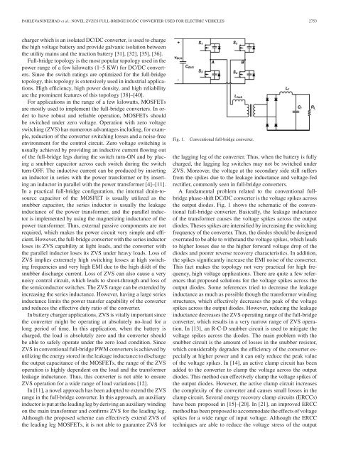
PAHLEVANINEZHAD et al.: NOVEL <strong>ZVZCS</strong> FULL-BRIDGE <strong>DC</strong>/<strong>DC</strong> CONVERTER USED FOR ELECTRIC VEHICLES 2753charger which is an isolated <strong>DC</strong>/<strong>DC</strong> converter, is used to chargethe high voltage battery and provide galvanic isolation betweenthe utility mains and the traction battery [31], [32], [35], [36].<strong>Full</strong>-bridge topology is the most popular topology used in thepower range of a few kilowatts (1–5 KW) for <strong>DC</strong>/<strong>DC</strong> converters.Since the switch ratings are optimized for the full-bridgetopology, this topology is extensively used in industrial applications.High efficiency, high power density, and high reliabilityare the prominent features of this topology [38]–[40].For applications in the range of a few kilowatts, MOSFETsare mostly used to implement the full-bridge converters. In orderto have robust and reliable operation, MOSFETs shouldbe switched under zero voltage. Operation with zero voltageswitching (ZVS) has numerous advantages including, for example,reduction of the converter switching losses and a noise-freeenvironment for the control circuit. Zero voltage switching isusually achieved by providing an inductive current flowing outof the full-bridge legs during the switch turn-ON and by placinga snubber capacitor across each switch during the switchturn-OFF. The inductive current can be produced by insertingan inductor in series with the power transformer or by insertingan inductor in parallel with the power transformer [4]–[11].In a practical full-bridge configuration, the internal drain-tosourcecapacitor of the MOSFET is usually utilized as thesnubber capacitor, the series inductor is usually the leakageinductance of the power transformer, and the parallel inductoris implemented by using the magnetizing inductance of thepower transformer. Thus, external passive components are notrequired, which makes the power circuit very simple and efficient.However, the full-bridge converter with the series inductorloses its ZVS capability at light loads, and the converter withthe parallel inductor loses its ZVS under heavy loads. Loss ofZVS implies extremely high switching losses at high switchingfrequencies and very high EMI due to the high di/dt of thesnubber discharge current. Loss of ZVS can also cause a verynoisy control circuit, which leads to shoot-through and loss ofthe semiconductor switches. The ZVS range can be extended byincreasing the series inductance. However, having a large seriesinductance limits the power transfer capability of the converterand reduces the effective duty ratio of the converter.In battery charger applications, ZVS is vitally important sincethe converter might be operating at absolutely no-load for along period of time. In this application, when the battery ischarged, the load is absolutely zero and the converter shouldbe able to safely operate under the zero load condition. SinceZVS in conventional full-bridge PWM converters is achieved byutilizing the energy stored in the leakage inductance to dischargethe output capacitance of the MOSFETs, the range of the ZVSoperation is highly dependent on the load and the transformerleakage inductance. Thus, this converter is not able to ensureZVS operation for a wide range of load variations [12].In [11], a novel approach has been adopted to extend the ZVSrange in the full-bridge converter. In this approach, an auxiliaryinductor is put at the leading leg by deriving an auxiliary windingon the main transformer and confirms ZVS for the leading leg.Although the proposed scheme can effectively extend ZVS ofthe leading leg MOSFETs, it is not able to guarantee ZVS forFig. 1.Conventional full-bridge converter.the lagging leg of the converter. Thus, when the battery is fullycharged, the lagging leg switches may not be switched underZVS. Moreover, the voltage at the secondary side still suffersfrom the spikes due to the leakage inductance and voltage-fedrectifier, commonly seen in full-bridge converters.A fundamental problem related to the conventional fullbridgephase-shift <strong>DC</strong>/<strong>DC</strong> converter is the voltage spikes acrossthe output diodes. Fig. 1 shows the schematic of the conventionalfull-bridge converter. Basically, the leakage inductanceof the transformer causes the voltage spikes across the outputdiodes. Theses spikes are intensified by increasing the switchingfrequency of the converter. Thus, the diodes should be designedoverrated to be able to withstand the voltage spikes, which leadsto higher losses due to the higher forward voltage drop of thediodes and poorer reverse recovery characteristics. In addition,the spikes significantly increase the EMI noise of the converter.This fact makes the topology not very practical for high frequency,high voltage applications. There are quite a few referencesthat proposed solutions for the voltage spikes across theoutput diodes. Some references tried to decrease the leakageinductance as much as possible though the transformer windingstructures, which effectively decreases the peak of the voltagespikes across the output diodes. However, reducing the leakageinductance decreases the ZVS operating range of the full-bridgeconverter, which results in a very narrow range of ZVS operation.In [13], an R-C-D snubber circuit is used to mitigate thevoltage spikes across the diodes. The main problem with thesnubber circuit is the amount of losses in the snubber resistor,which considerably degrades the efficiency of the converter especiallyat higher power and it can only reduce the peak valueof the voltage spikes. In [14], an active clamp circuit has beenadded to the converter to clamp the voltage across the outputdiodes. This method can effectively clamp the voltage spikes ofthe output diodes. However, the active clamp circuit increasesthe complexity of the converter and causes small losses in theclamp circuit. Several energy recovery clamp circuits (ERCCs)have been proposed in [15]–[20]. In [21], an improved ERCCmethod has been proposed to accommodate the effects of voltagespikes for a wide range of input voltage. Although the ERCCtechniques are able to reduce the voltage stress of the output