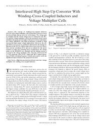
A Novel ZVZCS Full-Bridge DC/DC Converter Used ... - IEEE Xplore
A Novel ZVZCS Full-Bridge DC/DC Converter Used ... - IEEE Xplore
A Novel ZVZCS Full-Bridge DC/DC Converter Used ... - IEEE Xplore

You also want an ePaper? Increase the reach of your titles
YUMPU automatically turns print PDFs into web optimized ePapers that Google loves.
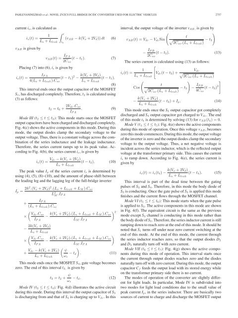
PAHLEVANINEZHAD et al.: NOVEL <strong>ZVZCS</strong> FULL-BRIDGE <strong>DC</strong>/<strong>DC</strong> CONVERTER USED FOR ELECTRIC VEHICLES 2757current i s , is calculated as∫1 ti s (t) =(v AB − k(V o +2V d )) dt (6)L s + L leak t 0v AB is given byv AB (t) = I PA(t − t 1 ). (7)2C soPlacing (7) into (6), i s is given byI PAi s (t) =(t − t 1 ) 2 − k(V o +2V d )(t − t 1 ).4(L s + L leak ).C so L s + L leak(8)This interval ends once the output capacitor of the MOSFETS 1 , has discharged completely. Therefore, t 2 is calculated using(3) as follows:t 2 = t 0 + 2V dc.C so. (9)I PAMode III (t 2 ≤ t ≤ t 3 ): This mode starts once the MOSFEToutput capacitors have been charged and discharged completely.Fig. 4(c) shows the active components in this mode. During thismode, the output diodes clamp the secondary voltage to theoutput voltage. Thus, there is a constant voltage across the combinationof the series inductance and the leakage inductance.Therefore, the series current ramps up to its peak value. Accordingto Fig. 4(b), the series current i s , is given byi s (t) = V dc − k(V o +2V d )(t − t 2 ). (10)L s + L leakThe peak value I p of the series current i s is determined byusing (4), (5), (8)–(10), and the amount of phase-shift betweenthe leading leg and the lagging leg of the full-bridge inverterI p = 2k2 .(V o +2V d ) 2 .(L s + L leak + L M ).C soL 2 M .I PAI PA+(L s + L leak ).C so(Vdc .C so× − k(V ) 2o +2V d ).(L s + L leak + L M ).C soL M .I PAI PA− 2k(V o +2V d )L s + L leak(Vdc .C so× − k(V )o +2V d ).(L s + L leak + L M ).C soL M .I PAI PA+ V ( )dc − k(V o +2V d ) ψ− t d . (11)L s + L leak ω sThis mode ends once the MOSFET S 4 , gate voltage becomeszero. The end of this interval t 3 , is given byt 3 = t 2 + ψ ω s− t d . (12)Mode IV (t 3 ≤ t ≤ t 4 ): Fig. 4(d) illustrates the active circuitduring this mode. During this interval the output capacitor of S 3is discharging from and that of S 4 is charging up to V dc .Inthisinterval, the output voltage of the inverter v AB, is given by()tv AB (t) =V dc − V dc Sin √2Cso .(L s + L leak ) − t 3− I PB2C so(t − t 3 ). (13)The series current is calculated using (13) as follows:[1Vi s (t) =V dc (t − t 3 )+ √ dcL s + L leak 2Cso .(L s + L leak )()Cost√2Cso .(L s + L leak ) − t 3− I PB4C so(t − t 3 ) 2 ]− k(V o +2V d )(t − t 3 )+I p . (14)L s + L leakThis mode ends once the S 3 output capacitor got completelydischarged and S 4 output capacitor got charged to V dc . The endof this mode t 4 is determined by solving (13) for v AB (t 4 )=0.Mode V (t 4 ≤ t ≤ t 5 ): Fig. 4(e) shows the active componentsduring this mode of operation. Once this voltage v AB , becomeszero this mode commences. During this mode, the output voltageof the inverter is zero and the output diodes clamp the secondaryvoltage to the output voltage. Thus, a net negative voltage isincident across the series inductor, which is the reflected outputvoltage at the transformer primary side. This causes the currenti s to ramp down. According to Fig. 4(e), the series current isgiven byi s (t) =i s (t 4 ) − k(V o +2V d )(t − t 4 ). (15)L s + L leakThis interval is part of the dead time between the gatingpulses of S 3 and S 4 . Therefore, in this mode the body diode ofS 3 is conducting. Once the gate pulse of S 3 is applied this modefinishes and the current flows through the MOSFET channel.Mode VI (t 5 ≤ t ≤ t 6 ): This mode starts when the gate pulseis applied to S 3 . The active components in this mode are shownin Fig. 4(f). The equivalent circuit is the same as the previousmode except S 3 channel is conducting in this mode rather thanthe body diode of S 3 . Therefore, the series inductor current is stillramping down to reach zero at the end of this mode. It should benoted that S 1 turns off under near zero current switching at theend of this mode. At the end of this mode, the current throughthe series inductor reaches zero, so that the output diodes D 2and D 3 naturally turn off with zero current.Mode VII (t 6 ≤ t ≤ t 7 ): Fig. 4(g) shows the active componentsduring this mode of operation. This interval starts oncethe current through output diodes reaches zero and the diodesnaturally turn off with zero current. During this mode, the outputcapacitor C f feeds the output load with its stored energy whileon the transformer primary side there is no current.The modes of operation of the converter are slightly differentfor light loads. In particular, Mode IV is subdivided intotwo modes for light load conditions due to the small value ofpeak current I p , in the series inductor. There are basically twosources of current to charge and discharge the MOSFET output