A Novel ZVZCS Full-Bridge DC/DC Converter Used ... - IEEE Xplore
A Novel ZVZCS Full-Bridge DC/DC Converter Used ... - IEEE Xplore
A Novel ZVZCS Full-Bridge DC/DC Converter Used ... - IEEE Xplore

Create successful ePaper yourself
Turn your PDF publications into a flip-book with our unique Google optimized e-Paper software.
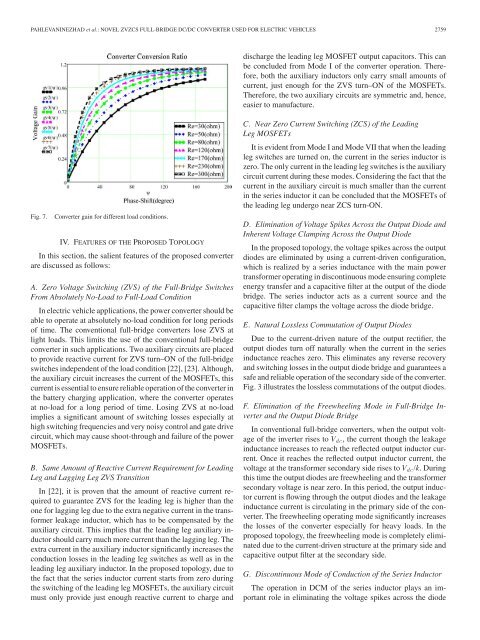
PAHLEVANINEZHAD et al.: NOVEL <strong>ZVZCS</strong> FULL-BRIDGE <strong>DC</strong>/<strong>DC</strong> CONVERTER USED FOR ELECTRIC VEHICLES 2759discharge the leading leg MOSFET output capacitors. This canbe concluded from Mode I of the converter operation. Therefore,both the auxiliary inductors only carry small amounts ofcurrent, just enough for the ZVS turn–ON of the MOSFETs.Therefore, the two auxiliary circuits are symmetric and, hence,easier to manufacture.Fig. 7.<strong>Converter</strong> gain for different load conditions.IV. FEATURES OF THE PROPOSED TOPOLOGYIn this section, the salient features of the proposed converterare discussed as follows:A. Zero Voltage Switching (ZVS) of the <strong>Full</strong>-<strong>Bridge</strong> SwitchesFrom Absolutely No-Load to <strong>Full</strong>-Load ConditionIn electric vehicle applications, the power converter should beable to operate at absolutely no-load condition for long periodsof time. The conventional full-bridge converters lose ZVS atlight loads. This limits the use of the conventional full-bridgeconverter in such applications. Two auxiliary circuits are placedto provide reactive current for ZVS turn–ON of the full-bridgeswitches independent of the load condition [22], [23]. Although,the auxiliary circuit increases the current of the MOSFETs, thiscurrent is essential to ensure reliable operation of the converter inthe battery charging application, where the converter operatesat no-load for a long period of time. Losing ZVS at no-loadimplies a significant amount of switching losses especially athigh switching frequencies and very noisy control and gate drivecircuit, which may cause shoot-through and failure of the powerMOSFETs.B. Same Amount of Reactive Current Requirement for LeadingLeg and Lagging Leg ZVS TransitionIn [22], it is proven that the amount of reactive current requiredto guarantee ZVS for the leading leg is higher than theone for lagging leg due to the extra negative current in the transformerleakage inductor, which has to be compensated by theauxiliary circuit. This implies that the leading leg auxiliary inductorshould carry much more current than the lagging leg. Theextra current in the auxiliary inductor significantly increases theconduction losses in the leading leg switches as well as in theleading leg auxiliary inductor. In the proposed topology, due tothe fact that the series inductor current starts from zero duringthe switching of the leading leg MOSFETs, the auxiliary circuitmust only provide just enough reactive current to charge andC. Near Zero Current Switching (ZCS) of the LeadingLeg MOSFETsIt is evident from Mode I and Mode VII that when the leadingleg switches are turned on, the current in the series inductor iszero. The only current in the leading leg switches is the auxiliarycircuit current during these modes. Considering the fact that thecurrent in the auxiliary circuit is much smaller than the currentin the series inductor it can be concluded that the MOSFETs ofthe leading leg undergo near ZCS turn-ON.D. Elimination of Voltage Spikes Across the Output Diode andInherent Voltage Clamping Across the Output DiodeIn the proposed topology, the voltage spikes across the outputdiodes are eliminated by using a current-driven configuration,which is realized by a series inductance with the main powertransformer operating in discontinuous mode ensuring completeenergy transfer and a capacitive filter at the output of the diodebridge. The series inductor acts as a current source and thecapacitive filter clamps the voltage across the diode bridge.E. Natural Lossless Commutation of Output DiodesDue to the current-driven nature of the output rectifier, theoutput diodes turn off naturally when the current in the seriesinductance reaches zero. This eliminates any reverse recoveryand switching losses in the output diode bridge and guarantees asafe and reliable operation of the secondary side of the converter.Fig. 3 illustrates the lossless commutations of the output diodes.F. Elimination of the Freewheeling Mode in <strong>Full</strong>-<strong>Bridge</strong> Inverterand the Output Diode <strong>Bridge</strong>In conventional full-bridge converters, when the output voltageof the inverter rises to V dc , the current though the leakageinductance increases to reach the reflected output inductor current.Once it reaches the reflected output inductor current, thevoltage at the transformer secondary side rises to V dc /k.Duringthis time the output diodes are freewheeling and the transformersecondary voltage is near zero. In this period, the output inductorcurrent is flowing through the output diodes and the leakageinductance current is circulating in the primary side of the converter.The freewheeling operating mode significantly increasesthe losses of the converter especially for heavy loads. In theproposed topology, the freewheeling mode is completely eliminateddue to the current-driven structure at the primary side andcapacitive output filter at the secondary side.G. Discontinuous Mode of Conduction of the Series InductorThe operation in <strong>DC</strong>M of the series inductor plays an importantrole in eliminating the voltage spikes across the diode