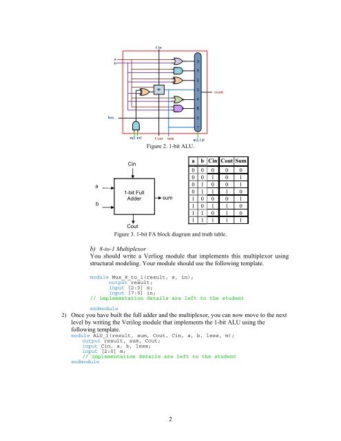
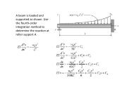
Figure 2. 1-bit <strong>ALU</strong>.abCin1-bit FullAddersumab Cin Cout Sum0 0 0 0 00 0 1 0 10 1 0 0 10 1 1 1 01 0 0 0 11 0 1 1 01 1 0 1 01 1 1 1 1CoutFigure 3. 1-bit FA block diagram and truth table.b) 8-to-1 MultiplexorYou should write a Verliog module that implements this multiplexor usingstructural modeling. Your module should use the following template.module Mux_8_to_1(result, s, in);output result;input [2:0] s;input [7:0] in;// implementation details are left to the studentendmodule2) Once you have built the full adder and the multiplexor, you can now move to the nextlevel by writing the Verilog module that implements the 1-bit <strong>ALU</strong> using thefollowing template.module <strong>ALU</strong>_1(result, sum, Cout, Cin, a, b, less, m);output result, sum, Cout;input Cin, a, b, less;input [2:0] m;// implementation details are left to the studentendmodule2
3) After you have designed the 1-bit <strong>ALU</strong>, you may choose to use 32 copies of thismodule to build the large 32-bit <strong>ALU</strong>. However, such approach is time consumingand requires a lot of effort in wiring-up these instances. Instead, consider building the32-bit <strong>ALU</strong> using 8-bit <strong>ALU</strong>s. In this case you need to wire only 4 instances. So,consider writing a Verilog module for an 8-bit <strong>ALU</strong> using the 1-bit <strong>ALU</strong> designed inthe previous step. Use the following template.module <strong>ALU</strong>_8(result, sum, Cout, Cin, a, b, less, m);output [7:0]result, sum;output Cout;input Cin;input [7:0]a, b, less;input [2:0] m;// implementation details are left to the student…endmodule4) Once you have built the 8-bit <strong>ALU</strong>, it is time to construct the 32-bit <strong>ALU</strong>. Use thefollowing template for this purpose.module <strong>ALU</strong>_32(result, a, b, m);output [31:0]result;input [31:0]a, b;input [2:0] m;// implementation details are left to the student…endmoduleTestingWrite a Verilog module to test your 32-bit <strong>ALU</strong>. The module should use the data given inTable II as a benchmark. Generate the timing diagram and estimate the maximum delay inyour design.a b mffff0000 h ff00ff00 h 000ffff0000 h ff00ff00 h 001ffff0000 h ff00ff00 h 010ffff0000 h ff00ff00 h 100ffff0000 h ff00ff00 h 10177665544 h 66554433 h 01177665544 h 66554433 h 11077665544 h 66554433 h 11111112222 h 33334444 h 11011112222 h 33334444 h 111ReportYour report should include detailed design, Verilog code for all modules including your testmodule(s), and timing diagram with proper justifications and discussions.3