ALU Design - FET
ALU Design - FET
ALU Design - FET

Create successful ePaper yourself
Turn your PDF publications into a flip-book with our unique Google optimized e-Paper software.
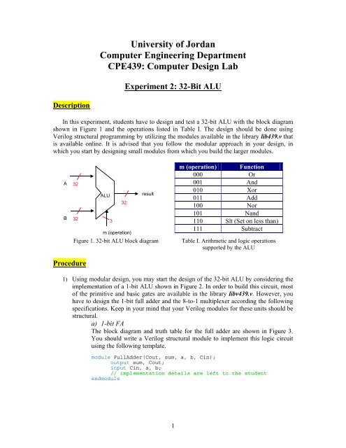
University of JordanComputer Engineering DepartmentCPE439: Computer <strong>Design</strong> LabExperiment 2: 32-Bit <strong>ALU</strong>DescriptionIn this experiment, students have to design and test a 32-bit <strong>ALU</strong> with the block diagramshown in Figure 1 and the operations listed in Table I. The design should be done usingVerilog structural programming by utilizing the modules available in the library lib439.v thatis available online. It is advised that you follow the modular approach in your design, inwhich you start by designing small modules from which you build the larger modules.AB32<strong>ALU</strong>result32323m (operation)Figure 1. 32-bit <strong>ALU</strong> block diagramm (operation) Function000 Or001 And010 Xor011 Add100 Nor101 Nand110 Slt (Set on less than)111 SubtractTable I. Arithmetic and logic operationssupported by the <strong>ALU</strong>Procedure1) Using modular design, you may start the design of the 32-bit <strong>ALU</strong> by considering theimplementation of a 1-bit <strong>ALU</strong> shown in Figure 2. In order to build this circuit, mostof the primitive and basic gates are available in the library libv439.v. However, youhave to design the 1-bit full adder and the 8-to-1 multiplexer according the followingspecifications. Keep in your mind that your Verilog modules for these units should bestructural.a) 1-bit FAThe block diagram and truth table for the full adder are shown in Figure 3.You should write a Verilog structural module to implement this logic circuitusing the following template.module FullAdder(Cout, sum, a, b, Cin);output sum, Cout;input Cin, a, b;// implementation details are left to the studentendmodule1
Figure 2. 1-bit <strong>ALU</strong>.abCin1-bit FullAddersumab Cin Cout Sum0 0 0 0 00 0 1 0 10 1 0 0 10 1 1 1 01 0 0 0 11 0 1 1 01 1 0 1 01 1 1 1 1CoutFigure 3. 1-bit FA block diagram and truth table.b) 8-to-1 MultiplexorYou should write a Verliog module that implements this multiplexor usingstructural modeling. Your module should use the following template.module Mux_8_to_1(result, s, in);output result;input [2:0] s;input [7:0] in;// implementation details are left to the studentendmodule2) Once you have built the full adder and the multiplexor, you can now move to the nextlevel by writing the Verilog module that implements the 1-bit <strong>ALU</strong> using thefollowing template.module <strong>ALU</strong>_1(result, sum, Cout, Cin, a, b, less, m);output result, sum, Cout;input Cin, a, b, less;input [2:0] m;// implementation details are left to the studentendmodule2
3) After you have designed the 1-bit <strong>ALU</strong>, you may choose to use 32 copies of thismodule to build the large 32-bit <strong>ALU</strong>. However, such approach is time consumingand requires a lot of effort in wiring-up these instances. Instead, consider building the32-bit <strong>ALU</strong> using 8-bit <strong>ALU</strong>s. In this case you need to wire only 4 instances. So,consider writing a Verilog module for an 8-bit <strong>ALU</strong> using the 1-bit <strong>ALU</strong> designed inthe previous step. Use the following template.module <strong>ALU</strong>_8(result, sum, Cout, Cin, a, b, less, m);output [7:0]result, sum;output Cout;input Cin;input [7:0]a, b, less;input [2:0] m;// implementation details are left to the student…endmodule4) Once you have built the 8-bit <strong>ALU</strong>, it is time to construct the 32-bit <strong>ALU</strong>. Use thefollowing template for this purpose.module <strong>ALU</strong>_32(result, a, b, m);output [31:0]result;input [31:0]a, b;input [2:0] m;// implementation details are left to the student…endmoduleTestingWrite a Verilog module to test your 32-bit <strong>ALU</strong>. The module should use the data given inTable II as a benchmark. Generate the timing diagram and estimate the maximum delay inyour design.a b mffff0000 h ff00ff00 h 000ffff0000 h ff00ff00 h 001ffff0000 h ff00ff00 h 010ffff0000 h ff00ff00 h 100ffff0000 h ff00ff00 h 10177665544 h 66554433 h 01177665544 h 66554433 h 11077665544 h 66554433 h 11111112222 h 33334444 h 11011112222 h 33334444 h 111ReportYour report should include detailed design, Verilog code for all modules including your testmodule(s), and timing diagram with proper justifications and discussions.3