Electrophoretic Photoresist Application for High ... - CS Mantech
Electrophoretic Photoresist Application for High ... - CS Mantech
Electrophoretic Photoresist Application for High ... - CS Mantech
Create successful ePaper yourself
Turn your PDF publications into a flip-book with our unique Google optimized e-Paper software.
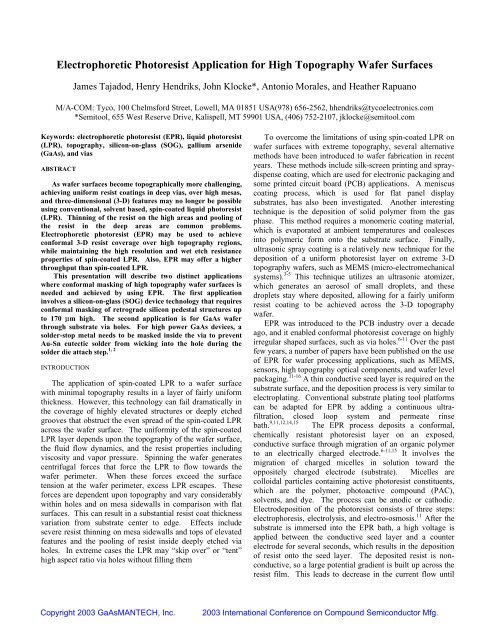
<strong>Electrophoretic</strong> <strong>Photoresist</strong> <strong>Application</strong> <strong>for</strong> <strong>High</strong> Topography Wafer SurfacesJames Tajadod, Henry Hendriks, John Klocke*, Antonio Morales, and Heather RapuanoM/A-COM: Tyco, 100 Chelms<strong>for</strong>d Street, Lowell, MA 01851 USA(978) 656-2562, hhendriks@tycoelectronics.com*Semitool, 655 West Reserve Drive, Kalispell, MT 59901 USA, (406) 752-2107, jklocke@semitool.comKeywords: electrophoretic photoresist (EPR), liquid photoresist(LPR), topography, silicon-on-glass (SOG), gallium arsenide(GaAs), and viasABSTRACTAs wafer surfaces become topographically more challenging,achieving uni<strong>for</strong>m resist coatings in deep vias, over high mesas,and three-dimensional (3-D) features may no longer be possibleusing conventional, solvent based, spin-coated liquid photoresist(LPR). Thinning of the resist on the high areas and pooling ofthe resist in the deep areas are common problems.<strong>Electrophoretic</strong> photoresist (EPR) may be used to achievecon<strong>for</strong>mal 3-D resist coverage over high topography regions,while maintaining the high resolution and wet etch resistanceproperties of spin-coated LPR. Also, EPR may offer a higherthroughput than spin-coated LPR.This presentation will describe two distinct applicationswhere con<strong>for</strong>mal masking of high topography wafer surfaces isneeded and achieved by using EPR. The first applicationinvolves a silicon-on-glass (SOG) device technology that requirescon<strong>for</strong>mal masking of retrograde silicon pedestal structures upto 170 Pm high. The second application is <strong>for</strong> GaAs waferthrough substrate via holes. For high power GaAs devices, asolder-stop metal needs to be masked inside the via to preventAu-Sn eutectic solder from wicking into the hole during thesolder die attach step. 1, 2INTRODUCTIONThe application of spin-coated LPR to a wafer surfacewith minimal topography results in a layer of fairly uni<strong>for</strong>mthickness. However, this technology can fail dramatically inthe coverage of highly elevated structures or deeply etchedgrooves that obstruct the even spread of the spin-coated LPRacross the wafer surface. The uni<strong>for</strong>mity of the spin-coatedLPR layer depends upon the topography of the wafer surface,the fluid flow dynamics, and the resist properties includingviscosity and vapor pressure. Spinning the wafer generatescentrifugal <strong>for</strong>ces that <strong>for</strong>ce the LPR to flow towards thewafer perimeter. When these <strong>for</strong>ces exceed the surfacetension at the wafer perimeter, excess LPR escapes. These<strong>for</strong>ces are dependent upon topography and vary considerablywithin holes and on mesa sidewalls in comparison with flatsurfaces. This can result in a substantial resist coat thicknessvariation from substrate center to edge. Effects includesevere resist thinning on mesa sidewalls and tops of elevatedfeatures and the pooling of resist inside deeply etched viaholes. In extreme cases the LPR may “skip over” or “tent”high aspect ratio via holes without filling themTo overcome the limitations of using spin-coated LPR onwafer surfaces with extreme topography, several alternativemethods have been introduced to wafer fabrication in recentyears. These methods include silk-screen printing and spraydispensecoating, which are used <strong>for</strong> electronic packaging andsome printed circuit board (PCB) applications. A meniscuscoating process, which is used <strong>for</strong> flat panel displaysubstrates, has also been investigated. Another interestingtechnique is the deposition of solid polymer from the gasphase. This method requires a monomeric coating material,which is evaporated at ambient temperatures and coalescesinto polymeric <strong>for</strong>m onto the substrate surface. Finally,ultrasonic spray coating is a relatively new technique <strong>for</strong> thedeposition of a uni<strong>for</strong>m photoresist layer on extreme 3-Dtopography wafers, such as MEMS (micro-electromechanicalsystems). 3-5 This technique utilizes an ultrasonic atomizer,which generates an aerosol of small droplets, and thesedroplets stay where deposited, allowing <strong>for</strong> a fairly uni<strong>for</strong>mresist coating to be achieved across the 3-D topographywafer.EPR was introduced to the PCB industry over a decadeago, and it enabled con<strong>for</strong>mal photoresist coverage on highlyirregular shaped surfaces, such as via holes. 6-11 Over the pastfew years, a number of papers have been published on the useof EPR <strong>for</strong> wafer processing applications, such as MEMS,sensors, high topography optical components, and wafer levelpackaging. 11-16 A thin conductive seed layer is required on thesubstrate surface, and the deposition process is very similar toelectroplating. Conventional substrate plating tool plat<strong>for</strong>mscan be adapted <strong>for</strong> EPR by adding a continuous ultrafiltration,closed loop system and permeate rinsebath. 9,11,12,14,15 The EPR process deposits a con<strong>for</strong>mal,chemically resistant photoresist layer on an exposed,conductive surface through migration of an organic polymerto an electrically charged electrode. 6-11,15 It involves themigration of charged micelles in solution toward theoppositely charged electrode (substrate). Micelles arecolloidal particles containing active photoresist constituents,which are the polymer, photoactive compound (PAC),solvents, and dye. The process can be anodic or cathodic.Electrodeposition of the photoresist consists of three steps:electrophoresis, electrolysis, and electro-osmosis. 11 After thesubstrate is immersed into the EPR bath, a high voltage isapplied between the conductive seed layer and a counterelectrode <strong>for</strong> several seconds, which results in the depositionof resist onto the seed layer. The deposited resist is nonconductive,so a large potential gradient is built up across theresist film. This leads to decrease in the current flow until
electrolysis stops (current reaches zero). This self-limitingbehavior results in a highly con<strong>for</strong>mal film electrodepositedfrom an aqueous emulsion solution on the order of 4-18µm. 11-14,15 The final thickness is dependent upon the bathcontents of a special thickness controlling (TC) chemical, thebath temperature, and the applied voltage. 11-14,15 Afterdeposition the wafer is rinsed, dried, and then baked causingthe compacted micelles to level into a smooth continuouslayer of resist.APPLICATIONSThe 170 µm high pedestal structures, as shown in Figure 1on silicon wafers, provide the basis <strong>for</strong> heterolithicmicrowave integrated circuit (HMIC) processing. 17 SomeHMIC designs require a highly conductive metal scheme,such as sputtered Ti/W-Ag-Ti/W, to be deposited over thepedestal region. This metal scheme is not self-aligning andselective removal of the metal from the top center of thepedestal region is desired. A con<strong>for</strong>mal resist mask isrequired in order to protect the metal films on the pedestal topperimeter edge, sidewalls, and base during the subsequentwet etch step. The silicon pedestals can be fabricatedutilizing a wet, anisotropic etch process 17 , which results insidewalls parallel to (111) planes and 55° sidewall angles, oran inductively coupled plasma (ICP) etch, which producesslightly retrograde sidewall profiles (see Figure 1).Figure 1: 170 µm high Si pedestal topography produced by an ICP etch.The slightly retrograde sidewalls require a con<strong>for</strong>mal resist coat that alsocovers the pedestal top perimeter.Figure 2: GaAs vias produced by reactive ion etching (RIE) using BCl 3 /Cl 2chemistry. The two via cross sections shown were cleaved and polished inperpendicular directions. Con<strong>for</strong>mal resist mask coverage is desired over thesidewalls including the retrograde portion.For high power GaAs devices, a positive photoresist maskis used to cover solder-stop metal inside the via holes whilethis metal is wet etched from the back-side leaving an inertAu surface <strong>for</strong> subsequent Au-Sn eutectic solder die attach.The oxidized solder-stop metal lining the via sidewallsprevents Au-Sn from the solder pre-<strong>for</strong>m from wicking intothe hole during die attach. 1,2 The holes can be up to 100 µmdeep as shown in Figure 2. For low aspect ratio vias, a thick,positive LPR has been successfully used <strong>for</strong> the past severalyears. Recently, there has a been a strong ef<strong>for</strong>t to reduce viasize and increase aspect ratio, which can result in a coverageproblems when trying to use LPR. 1,2 EPR can be used toaddress this issue.EXPERIMENTAL & RESULTS: HMIC Si PEDESTAL STRUCTURESFive 100 mm diameter Si wafers with pedestals fabricatedusing a wet, anisotropic etch process were sent to Semitool,Inc. <strong>for</strong> coating with PEPR 2400 photoresist 18 , which is apositive EPR with negatively charged micelles available fromthe Shipley Company. The PEPR 2400 was deposited in aSemitool semiautomatic, single wafer ECD (electro-chemicaldeposition) plat<strong>for</strong>m fitted with an EPR reactor. 11 Thedeposition parameters, such as temperature, filtration,voltage, current, and the PEPR 2400 TC plasticizerconcentration were maintained at Semitool’s process ofrecord conditions. The wafers, which were held horizontallywith the Ti/W-Ag-Ti/W layer facing downward in the ECDchamber, were rotated during the deposition process, whichtook less than 2 minutes per wafer. After deposition thewafers were baked on a hotplate at about 100°C <strong>for</strong> 10 min toremove moisture from the film and smooth the film surface.Con<strong>for</strong>mal PEPR 2400 coatings over the 170 µm highpedestals covered with the Ti/W-Ag-Ti/W layers wereachieved on all five wafers.The wafer surfaces were inspected using a SEM (scanningelectron microscope), and coat uni<strong>for</strong>mity appeared to beexcellent including the sidewall, top, and edge coverage. Thedeposited resist layer had a uni<strong>for</strong>m and shiny appearance onall five wafers. Figure 3 shows SEM images of the PEPRlayer covering the underlying structures. Smooth, continuouscoverage of resist film was achieved over all of the analyzedfeatures. About 70% of the average thickness wasmaintained over even the most challenging feature, a squaretopped plateau with sharp outside corners. Typical coverageover convex corners is slightly thinner than the averagethickness because of rounding that occurred during the bakestep.Alignment and exposure were carried out on a CanonPLA-501F broadband contact/ proximity mask aligner.Instead of using the Shipley recommended sodium carbonatedeveloper with Photoposit 7412 Defoamer 18 , 0.26 normalMIF developer, which is TMAH (tetra-methyl ammoniumhydroxide) based, was used. The developed areas werecompletely open, but the sharpness of the resolved patternwas not optimized.The wafers were then subjected to a Ti/W wet etchcomposed of hydrogen peroxide and EDTA (ethylenediamine tetra-acetic acid) at room temperature (RT), but theetch did not initiate even though it was compatible with thePEPR mask. Microscopic inspection did not reveal any
obvious clues concerning etch initiation. At first resist scumor a monolayer organic film was suspected to be preventingetch initiation. A couple wafers were stripped free of thePEPR and immersed in this wet etch solution. Thepreviously shiny Ti/W film now had a dull brownishappearance. Auger surface and depth analysis showed strongsignals <strong>for</strong> Ti and O at and near the film surface. Titaniumoxidizes more readily than other metals, and the surface ofthe Ti layer was anodized during the EPR deposition process.In this case oxidation of the seed layer occurred in addition tothe electrolysis reaction. A 30 sec buffered oxide etch (BOEcontaining HF) was found to etch through the Ti oxide layer,so that Ti/W etch could be subsequently used after a quickde-ionized (DI) water rinse. The Ag was also etched by theRT hydroxide peroxide/ EDTA solution.Figure 3: SEM images of PEPR 2400 coverage of wet etched pedestals.The second iteration of this investigation will involvedepositing PEPR 2400 over Si pedestal structures withslightly retrograde sidewalls prepared using ICP (see Figure1). EPR deposition may be the only method that ensures100% resist coverage of the retrograde sidewalls because itdoes not have line of sight limitations.Ni/P solder-stop layer was immersed in a RT 1 HCl: 1 H 2 Osolution to remove the surface oxide layer. During thedeposition the thin wafer/ carriers were rotated to improveuni<strong>for</strong>mity and help prevent oxygen gas generated during theelectrolysis reaction from becoming trapped inside the vias.After deposition the samples were baked on a hotplate aspreviously described.Prior to the exposure and develop steps, the depositedPEPR film thickness could not be measured. Using a SussMA150 i-line (365 nm) backside contact/ proximity maskaligner, it was determined that a dose of 2000 mJ/cm 2 (50mW/cm 2 <strong>for</strong> 40 sec) provided sufficient exposure through thePEPR film. A backside dice street mask was used <strong>for</strong> theexposure experiment. To clear the exposed PEPR, a 3 minRT, immersion develop with agitation was done using aTMAH based developer. The developed areas were descummedin an oxygen plasma generated within a barrelasher. A Tencor P-11 surface depth profiler was used tomeasure the resist thickness at five points (near major flat,near minor flat, center, opposite major, and opposite minor)across several of the wafers on the backside surface using theopen dice streets. The average PEPR thickness per waferranged from 9.5-10.5 µm with a TTR (total thickness range)across an individual wafer of approximately 3µm.After de-scum the Ni/P was removed from the dice streetsusing a RT, dilute ferric chloride wet etch (compatible withPEPR) <strong>for</strong> approximately 45 sec as shown in Figure 4. Thevery thin Pd catalyst layer was then removed using aconcentrated sulfuric acid/ hydrogen peroxide mixture (1H 2 SO 4 : 1 H 2 O 2 : 3 H 2 O) at RT <strong>for</strong> 15 sec. Un<strong>for</strong>tunately, theresist mask was attacked and undercut during this etch step asshown in Figure 5. Klocke and Steeper previously showedthat PEPR 2400 can stand up to a dilute sulfuric acid/hydrogen peroxide mixture used to etch a sputtered copperseed layer. 11 The gold was then removed from the dice streetsusing a RT KI/I 2 based etch solution compatible with thePEPR mask.EXPERIMENTAL & RESULTS: GaAs THROUGH SUBSTRATE VIASAt M/A-COM two sets of GaAs wafers were mounted onsapphire carriers with Staystik 336T thermoplastic temporarybonding adhesive. The backside thinning (100 µm), via etch,and electroplate steps have been described previously. 1,2 Thehigh aspect ratio vias had a backside surface opening of about90 µm and a front-side opening adjacent to the bond pad ofabout 50 µm (see Figure 1). 2 After the etch, photomask stripand clean, and electrodeposition steps, a blanket electrolessNi/P solder-stop layer (very low P content, ≈0.1 µm) wasdeposited onto the backside, 3.0 µm thick electroplated goldlayer using a dilute PdCl 2 based catalyst solution. 1,2At Semitool the PEPR 2400 was deposited onto theelectroless Ni/P solder-stop layer (anode) utilizing theEquinox ECD plat<strong>for</strong>m with the wafer holder adapted <strong>for</strong> thethicker sapphire carriers. Prior to deposition the electrolessFigure 4: Backside wafer surface after dice street mask expose, develop, descum,and dilute ferric chloride etch. The light areas are exposed metal (Pdspots on Au) and the dark areas are the PEPR 2400 mask.Figure 5: Backside wafer surface after RT, 15 sec 1 H 2 SO 4 : 1H 2 O 2 : 3 H 2 Oimmersion etch to remove Pd. Au is shown within the dice streets. The darkPEPR mask areas have been attacked & undercut by the etch solution.
The goal of this evaluation was to determine if PEPR2400 could be used to replace the thick LPR <strong>for</strong> covering thehigh aspect ratio via sidewalls. The sidewalls need to becovered when the dice streets are etched and also when thesolder-stop Ni/P layer is removed from the backside surfaceleaving an exposed electroplated gold layer <strong>for</strong> Au-Sneutectic solder die attach. It may be possible to utilize a moredilute sulfuric acid / peroxide mixture to remove the very thinPd catalyst layer without attacking the PEPR. Also, mostGaAs power device wafer facilities use either sputtered Ti orTi/W <strong>for</strong> the solder-stop layer, and the PEPR has been shownto be compatible with some wet etch solutions <strong>for</strong> these twotypes of solder-stop layers.In addition to the etch undercut issue, we observedpinholes in the deposited PEPR 2400 film within some ofthe vias as shown in Figure 6. For all of the wafers, over95% of high aspect ratio vias from across the experimentwafers showed excellent con<strong>for</strong>mal coverage. Most of thepinholes appeared to be concentrated near the center of thebackside surface. Wafer rotation effectively removes gasbubbles from the outer edges of the wafer. Bubbles and theresulting pinholes on a substrate surface typically result fromcontamination or poor wet-ability of the underlyingconductive layer. <strong>Electrophoretic</strong> photoresist processes aresensitive to the surface properties of the substrate. Semitoolhas demonstrated pinhole free depositions on other substrates.With further optimization of precleaning and depositionprocedures, pinhole free coatings should be attainable <strong>for</strong>GaAs wafer backside via applications as well.(a) PEPR covering all vias (b) 1 pinhole, 2 good (c) 1 pinhole, 1 goodFigure 6: Pinholes noted within some backside vias. The pinholes may havebeen caused from gas bubbles trapped within the vias.CONCLUSIONShipley PEPR 2400 is a positive, i-line EPR that iscompatible with contact/ proximity mask alignment andexposure systems. The developer and stripper are differentthan what is currently used <strong>for</strong> wafer spin-coated LPR, but itis commercially available and can be easily integrated into awafer facility. The deposition tool is slightly more complexthan a conventional electroplating system. However, acommercialized system and process is available fromSemitool, Inc. 19The PEPR process delivered excellent con<strong>for</strong>malcoatings with very uni<strong>for</strong>m thickness, including on the sharptop edge of the Si pedestals. The thickness is self-limitingand appeared shiny and without pinholes. PEPR was alsofound to be a promising candidate <strong>for</strong> masking high aspectratio through wafer vias <strong>for</strong> the GaAs application. The viawalls could be masked, and the dicing streets could bedefined <strong>for</strong> subsequent wet etch steps. However, thispositive, anodic EPR was found to be incompatible with aconcentrated sulfuric acid/ hydrogen peroxide etch solutionused <strong>for</strong> the thin Pd catalyst layer removal. Furtherdevelopment is needed <strong>for</strong> a Pd etch chemistry that iscompatible PEPR 2400.ACKNOWLEDGEMENTS: The authors thank the following people fromM/A-COM, Semitool, & Shipley <strong>for</strong> their support: Peggy Barter, Carl Bunis,David Danzilio, Bob Forman, Joel Goodrich, Thomas Lepkowski, MarkMahoney, Gabe Rojano, Jill Steeper, Costas Varmazis, & Erik Young.REFERENCES:1 C. Varmazis, G. D’urso, and H. Hendriks, “How to Process the Backside ofGaAs Wafers”, Semicond. Internat. 23-14, 87 (2000).2 H. Hendriks, A. Hanson, T. Lepkowski, A. Quaglietta, and B. Patel,“Benefits and Challenges in Decreasing GaAs Through Substrate Via Sizeand Die Thickness”, GaAs MANTECH Conf. 2002, p. 105-109.3 T. L. Luxbacher and A. Mirza, “Spray Coating <strong>for</strong> MEMS, Interconnect, &Advanced Packaging <strong>Application</strong>s”, <strong>High</strong> Density Interconnect 2-5, p. 36-41(1999).4 A. Suriad, V. Sharma, and T. Luxbacher, “Photolithography onMicromachined 3-D Surfaces using Spray Coating Technology”, Proc. IEEEInternat. MEMS Workshop 2001.5 B. Wieder, C. Brubaker, D. Hornik, and N. Nodes, “Spray Coating: NewCoating Method on MEMS with Metal Surfaces”, Sensor Expo 2002, to bepublished.6 H. Nakahara, “Electrodeposition of Primary <strong>Photoresist</strong>s”, Electronic Pack.& Prod., Feb. 1992, p. 66-68.7 J. Diekmann, “Lithography and Photofabrication”, in Electronic Materialsand Processes Handbook (ed. C. A. Harper and R. N. Sampson), McGrawHill, New York, p. 10.22-10.47 (1994).8 T. Jacob, U. Lacher, and D. Kapp-Schwoerer, “Liquid Resist Allows SizeReduction”, Electronic Pack. & Prod., Nov. 1996, p. 27-34.9 N. B. Feilchenfeld, “Imaging” in Printed Circuits Handbook (ed. C. F.Coombs), McGraw Hill, New York, p. 17.7-17.17 (1996).10 E. Hayes, “Primary Imaging Resist” in Printed Circuit Board MaterialsHandbook (ed. M. W. Jawitz), McGraw Hill, New York, p. 14.13-14.15(1997).11 J. Klocke and J. Steeper, “Patterning Three-Dimensional Structures onWafers with <strong>Electrophoretic</strong> <strong>Photoresist</strong>”, 2002 Pan Pacific Symp. Conf.Proceed. (SMTA), p. 35-40.12 P. Kersten, S. Bouwstra, and J. W. Petersen, “Photolithography onmicromachined 3D surfaces using electrodeposited photoresists”, Sensorsand Actuators A 51, p. 51-54 (1995).13 S. Linder, H. Baltes, F. Gnaedinger, and E. Doering, “Photolithograhpy inAnistropically Etched Grooves”, Proceed. IEEE Internat. MEMs Workshop1996, p. 38-43.14 M. Heschel and S.Bouwstra, “Con<strong>for</strong>mal Coating by <strong>Photoresist</strong> of SharpCorners of Anistropically Etched Through-Holes in Silicon”, Internat. Conf.Solid-State Sensors & Actuators 1997, p. 209-212.15 E. Boellaard, P. N. Pham, L. van den Brekel, and J. N. Burghartz, “ RF-Devices Realized in MEMS by Using Electrodepositable <strong>Photoresist</strong>”,Proceed. SAFE 2001, p. 1-7, www.stw.nl/safe/proc2000/index.16 V. G. Kutchoukov, E. Boellaard, J. R. Mollinger, and A. Bossche, “NewFabrication Technology <strong>for</strong> Wafer-Through Hole Interconnects”, Proceed.SeSens 2001, p. 813-817, www.stw.nl/sesens/proc-2000/index.17 P. Chinoy, N. Jain, P. Li, J. Goodrich, and C. Souchuns, “Manufacture ofLow Loss Microwave Circuits Using HMIC Technology”, 1994 IEEE MTT-S Digest, p. 1137-1140.18 PEPR 2400 Process Manual, Shipley Company, Malborough, MA (2001).19 D. Paine, J. Klocke and J. Steeper, “Electrodeposited Resist – AComparison Between Positive and Negative Resist”, NEPCON West 2002Conference Proceedings, p. 265-269


