Characterization of Electroplated Gold for Back-Side ... - CS Mantech
Characterization of Electroplated Gold for Back-Side ... - CS Mantech
Characterization of Electroplated Gold for Back-Side ... - CS Mantech

You also want an ePaper? Increase the reach of your titles
YUMPU automatically turns print PDFs into web optimized ePapers that Google loves.
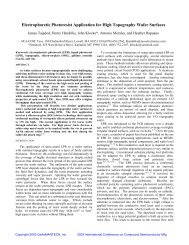
A standard least squares regression analysis wasper<strong>for</strong>med using JMP statistical s<strong>of</strong>tware package todetermine which parameters had an effect on the platingcon<strong>for</strong>mality. Figure 2 shows the results <strong>of</strong> the regressionanalysis per<strong>for</strong>med <strong>for</strong> the wafer edge data.Figure 2: Regression analysis results (leverage plots)(a)Whole Model Test(b) Effect <strong>of</strong> agitationLeverage plots and the Prob>F value give a goodidea <strong>of</strong> whether or not a factor has an effect on theresponse variable. A Prob>F less than 0.05 is evidence inthe Whole-Model Test that at least one <strong>of</strong> the factors beinginvestigated has an effect on the response variable.Further evidence that at least one <strong>of</strong> the factors has aneffect on the response variable is displayed in the leverageplot <strong>for</strong> the Whole-Model Test. If the 95% confidenceintervals, represented by the dashed curves, intersect themean <strong>of</strong> the response (0.24 represented by dashed line)there is evidence that there is at least one significant factorin the model. 25Figure 2(a) shows a leverage plot <strong>for</strong> the WholeModel Test. A Prob>F value <strong>of</strong> ~0.03 and the fact that theconfidence interval intersects the mean <strong>of</strong> the response isevidence that at least one <strong>of</strong> the factors investigated has asignificant effect on con<strong>for</strong>mality.To determine which <strong>of</strong> the factors investigated hasan effect on the con<strong>for</strong>mality the same analysis isper<strong>for</strong>med on the leverage plots <strong>for</strong> the individual factors.The leverage plot <strong>for</strong> agitation vs. con<strong>for</strong>mality has aProb>F value <strong>of</strong> 0.0085 (F values <strong>for</strong> the dutycycle and frequency factors do not present evidence <strong>of</strong> aneffect on con<strong>for</strong>mality in the ranges investigated.The con<strong>for</strong>mality <strong>of</strong> the plated film improves withincreased agitation and decreased current density. Thissuggests that there is a reduced number <strong>of</strong> gold ionsavailable <strong>for</strong> plating at the bottom <strong>of</strong> the via compared tothe back-side surface due to mass transfer limitations.(c)Effect <strong>of</strong> duty cycle(d) Effect <strong>of</strong> frequency
SUMMARYTwo rounds <strong>of</strong> experiments were per<strong>for</strong>med todetermine optimal process conditions <strong>for</strong> goldelectroplating <strong>for</strong> back-side processing <strong>of</strong> GaAs wafers.The goal <strong>of</strong> the experiments was achieving a con<strong>for</strong>malgold plated film in the back-side via. The first experimentinvestigated the effect <strong>of</strong> plating current density on thecon<strong>for</strong>mality <strong>of</strong> the plated film. Results indicate thatdecreasing current density improves the con<strong>for</strong>mality <strong>of</strong>the plated film.A statistically designed experiment was per<strong>for</strong>medto characterize the effects <strong>of</strong> frequency, duty cycle, andagitation rate on the con<strong>for</strong>mality <strong>of</strong> the plated film.Results show that increasing the agitation rate improvesthe con<strong>for</strong>mality <strong>of</strong> the plated film while the frequency andduty cycle did not show an effect over the rangesinvestigated.The results obtained in these two experimentssuggest that there is a reduced number <strong>of</strong> gold ionsavailable <strong>for</strong> plating in the bottom <strong>of</strong> the via compared tothe back-side surface due to mass transfer limitations.Further experimentation should focus onunderstanding the effects <strong>of</strong> mass transfer and chargetransfer on the non-con<strong>for</strong>mality <strong>of</strong> the gold plated film.REFERENCES:1 R. Williams, Modern GaAs Processing Techniques, Artech House, Inc.,Norwood, MA, 1990.2 D. Gupta, IEEE Trans. Comp., Pack., & Manuf. Tech. A 18, 82 (1995).3 C. L. Pillote, M. E. Grupen-Shemansky, S. P. Beaudoin, T. S. Cale,GaAs MANTECH Conf. 1997, p. 22-25.4 S. Aoki, H. Someta, S. Yokokawa, K. Ono, T. Hirose, and Y. Ohashi,1997 IEEE MTT-S Digest, p. 731-734.5 O. Vendier, S. George, J. P. Fraysse, E. Rogneaux, C. Deveron, J. L.Cazaux, D. Floriot, N. Caillas-Devignes, H. Blanck, W. Doser, P.Auxemery, W. de Ceuninck, R. Peterson, N. Haese, and P. A. Rolland,2000 IEEE GaAs Digest, p. 157-159.6 K. Sumitani, M. Komaru, M. Kobiki, Y. Higaki, Y. Mitsui, H. Takano,and K. Nishitani, 1989 IEEE GaAs IC Symp., p. 207-210.7 K. Okaniwa, T. Ishikawa, K. Kosaki, M. Komaru, Y. Notani, M. Kokiki,T. Mitsui, S. Orisaka, and N. Nishitani, 1990 IEEE GaAs IC Symp., p.233-236.8 K. J. Nordheden, D. W. Ferguson, and P. M. Smith, J. Vac. Sci Technol.B 11, 1879 (1993).9 T. Ishikawa, K. Okaniwa, M. Komaru, K. Kosaki, and Y Mitsui, IEEETrans. Electron Dev. 41, 3 (1994).10 L. W. Wang, J. J. Komiak, M. Y. Kao, D. E. Houston, D. P. Smith, andK. J. Nordheden, 1994 IEEE IEDM, p. 203-206.11 R. L Hale, GaAs MANTECH Conf. 1996, p. 164-167.12 P. Harris, D. Boone, M. King, J. Stidham, G. Bronson, K. Decker, andS. Subbarao, GaAs MANTECH Conf. 1997, p. 34-37.13 K. J. Nordheden, X. D. Hua, Y. S. Lee, L. W. Yang, D. C. Streit, and H.C. Chen, J. Vac. Sci Technol. B 17, 138 (1999).14 J. Lee, H. Tsai, Y. S. Chang, and R. T. Huang, GaAs MANTECH Conf.2000, p. 71-74.15 R. Szweda, III-V Review 13-5, 48 (2000).16 P. S. Nam, L. M. Ferreira, T. Y Lee, and K. N. Tu, J. Vac. Sci. Technol.B 18, 2780 (2000).17 A. Bavin, Solid State Tech. 44-7, 145 (2001).18 C. Varmazis, G. S. D’urso, and H. Hendriks, Semicond. Internat., 23-14, 87 (2000).19 H. Hendriks, J. Crites, G. D’urso, R. Fox, T. Lepkowski, and B. Patel,GaAs MANTECH Conf. 2001, p. 181-184.20 Puippe, J. C. and Leaman, F. (ed.), Theory and Practice <strong>of</strong> Pulse Plating,American Electroplaters and Surface Finishing Society, Orlando, FLA,1986.21 W. J. Dauksher, D. J. Resnick, W. A. Johnson, and A. W. Yan<strong>of</strong>,Microelectronic Eng. 23, 235 (1994).22 M. Schlesinger and M. Paunovic (ed.), Modern Electroplating FourthEdition, John Wiley & Sons, Inc., New York, 2000.23 C. Orlando, J. Goodrich, and E. L Gosselin, GaAs MANTECH Conf.2001, p. 189-191.24 H. Hendriks, A. Hanson, T. Lepkowski, A. Quaglietta, and B. Patel, tobe presented at GaAs MANTECH Conf. 2002.25 JMP Statistics and Graphics Guide, Version 3.1, SAS Institue Inc.,Cary, NC, USA, 1995, p. 139-175