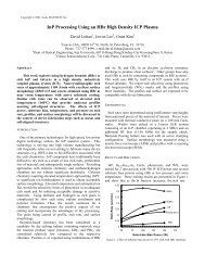
Stress and Other Challenges with Evaporated Ni-Cr ... - CS Mantech
Stress and Other Challenges with Evaporated Ni-Cr ... - CS Mantech
Stress and Other Challenges with Evaporated Ni-Cr ... - CS Mantech

Create successful ePaper yourself
Turn your PDF publications into a flip-book with our unique Google optimized e-Paper software.
<strong>Stress</strong> <strong>and</strong> <strong>Other</strong> <strong>Challenges</strong> <strong>with</strong> <strong>Evaporated</strong> <strong>Ni</strong>-<strong>Cr</strong> Thin Film ResistorsUsed in the Manufacture of ASICsNecmi Bilir <strong>and</strong> Long DoSkyworks Solutions, Inc., Sunnyvale Operations1230 Bordeaux Drive, Sunnyvale, CA 94089Keywords:thin film resistor, resistivity, <strong>Ni</strong>-<strong>Cr</strong>, TaN, stressSUMMARY:This paper studied the change in the characteristics ofthe <strong>Ni</strong>-<strong>Cr</strong> thin film resistors developed at theSunnyvale facility of Skyworks Solutions,(formerlyknown as NDI-Alpha Industries), <strong>with</strong> the number ofdepositions from the same source melt, as well as theeffects of sputter etch cleaning, oxygen plasma etch,HCl dip <strong>and</strong> regular annealing.HISTORY:The <strong>Ni</strong>-<strong>Cr</strong> thin film resistors are used as analternative to TaN resistors, due to the lower TCR (1)<strong>and</strong> higher stability against baking <strong>and</strong> plasma attacksof <strong>Ni</strong>-<strong>Cr</strong>. It is also possible to do in situ processmonitoring during evaporation.The difference between the composition of theevaporated <strong>Ni</strong>-<strong>Cr</strong> films <strong>and</strong> composition of the sourcematerial has been reported in earlier studies (2) . Sincechromium has a higher vapor pressure than nickel,the actual films contain more <strong>Cr</strong>, making the sourceget richer in nickel, after each run. During the periodof process development <strong>and</strong> the earlier days of lowervolume production levels, there were quite frequentsource material additions to the “melt” in theevaporators, as well as quite frequent replacement ofthe melts <strong>with</strong> the newly made ones. Therefore, theissue of compositional change of the melt <strong>and</strong> theresulting change in the composition of the films thatwere deposited in the later runs, came up veryseldom, if ever.PROBLEM:Only after the production volume increased to“hundreds of wafers per week”, <strong>and</strong> the evaporatorsstarted running multiple daily runs, did we startnoticing that the thickness of the deposited films wasdecreasing for the same resistance target value of theresistors, <strong>with</strong> the later runs from the same startingmelt. The source melt becoming richer in nickel (<strong>and</strong>more conductive) would have to be deposited thinner,for the same process specifications.The thinner <strong>Ni</strong>-rich films were also much moresusceptible to attack during the subsequent “acidcleaning steps” of the wafers <strong>with</strong> dilute HCl dip,leading to the formation of “mouse-bite” defects onthe wafers. (See figs.-1 <strong>and</strong> -2 below, of actual <strong>and</strong>intentionally produced mouse-bite defects on some<strong>Ni</strong>-<strong>Cr</strong> resistors.)Stoichiometric changes in the film also affect thecompressive stress in the film, changing from higherstress levels to lower, as the melt <strong>and</strong> the filmbecome richer in nickel. Obviously the films <strong>with</strong>greater stress will also have greater tendency ofpeeling-off of the wafers. However, the stress effectsare much less serious compared to the acid attack, atleast <strong>with</strong>in the compositional changes we have beenexperiencing.
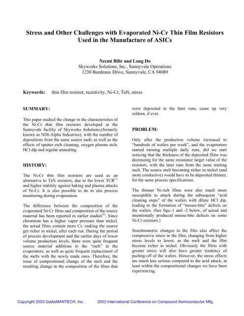
Figure-1: After two consecutive acid dipsFigure-2: After four consecutive acid dipsSOLUTION:We determined that the films deposited from thenewly made <strong>Ni</strong>-<strong>Cr</strong> melt (presumably <strong>with</strong> exactly80%-20% proportions) in the earlier runs did nothave any problems <strong>with</strong> the acid attack, despite theirhigher film stress. The mouse-bites appeared always<strong>with</strong> the later depositions, as the source-melt <strong>and</strong> theresistor films got richer in nickel.Therefore, the corrective action was to limit thenumber of depositions from the same starting sourcemelt, <strong>and</strong> to reduce the duration of the acid dip,<strong>with</strong>out risking the effectiveness of the cleaningprocess.EXPERIMENTAL RESULTS:1- TYPICAL PROCESS DATA: (from thesnapshots of the process at different time periods)<strong>Ni</strong>-<strong>Cr</strong> RESISTORS:Resistivity Thickness Power <strong>Stress</strong>(ohm/sq.) (Å) (kW) (e9 dyne/cm 2 )20 580-700 8 5.5-13.550 190-240 8 5.0-11.0TaN RESISTORS:20 850-1050 15 3.0-7.150 500- 610 10 3.9-7.6Note 1: The thickness values are as read from the crystaldeposition monitors of the evaporators- all CHA’s.Note 2: The stress values are negative (compressive).Note 3: TaN resistors were deposited in PE-4450 Sputterstation.2- RESISTOR DAMAGE DATA (Only <strong>Ni</strong>-<strong>Cr</strong>Resistors 3 ):Several silicon test wafers selected among theprocess monitor wafers were measured using the 4-point probe before starting the experiments, <strong>and</strong> aftereach one of the intentional damage test steps, givenbelow: (The plasma damage tests to Wafer-1 <strong>and</strong>Wafer-2 was done using YES downstream plasmaasher, while the remaining wafers were all done inthe Branson-IPC barrel etcher.) All numerical resultsare the median values measured on five locations oneach wafer.The HCl dip was for 30 seconds in a 1:10 HCl:DImixture, <strong>and</strong> bake was done in convection ovens for40 minutes, at 250 C.The test results led to the following conclusions:1- The actual change in the sheet resistance values(these are silicon process monitor wafers) is <strong>with</strong>in3% in the worst case, 2- The damage is much less forthe thicker films (20 ohm/sq), <strong>and</strong> 3- Downstreamplasma asher has practically no effect.
Wafer Initial After After AfterNumber Rs de-scum HCl Dip Bake1 45.9 46.1 46.1 46.12 45.9 46.0 46.3 46.13 46.0 47.6 47.6 47.44 45.9 47.7 47.5 47.15 24.8 24.9 25.0 25.36 19.5 19.7 19.8 19.73- SPUTTER-ETCH DAMAGE (<strong>Ni</strong>-<strong>Cr</strong>Resistors only):The following data show the change in the sheetresistance values of nominally 50 ohm/sq siliconmonitor wafers, after a 30 sec de-scum in YESdownstream asher, followed by 500 W sputter etch inPE-4450 sputter station, in a nitrogen/argonatmosphere, for the given durations.Resistance 2-minutes 3-minutes 4-minutes(ohm/sq)Before Etch 46.9 46.6 47.0After Etch 56.9 64.9 76.5STRESS VARIATION: (<strong>Ni</strong>-<strong>Cr</strong> films from thesame evaporator, <strong>and</strong> all 20 ohm/sq, nominal)The data below are the stress measurements done onthe silicon process monitor wafers, from consecutiveproduction runs, starting <strong>with</strong> a new source melt, <strong>and</strong>continuing after adding new source material to themelt.Deposition Sheet Film FilmNumber DATE Resistance Thickness <strong>Stress</strong>0 10/04/02 19.5 606 No data(New starting melt)1 10/07/02 19.6 603 No data(No stress measurement was done)2 10/07/02 19.8 596 10.10 e93 10/07/02 20.3 592 9.10 e94 10/08/02 20.4 591 8.85 e95 10/11/02 19.8 585 8.35 e96 10/11/02 19.7 588 7.61 e97 10/14/02 20.2 587 6.65 e98 10/14/02 20.4 570 6.17 e99 10/14/02 19.5 581 6.77 e910 10/14/02 19.6 568 7.00 e911 10/14/02 19.8 551 5.60 e9(At this point, added new <strong>Ni</strong>-<strong>Cr</strong> pellets)0 10/15/02 20.5 598 10.80 e91 10/15/02 20.0 595 8.90 e92 10/15/02 20.0 578 7.84 e93 10/15/02 20.0 577 7.29 e9Conclusion: The increase in the sheet resistancecorresponds to an approximate 20 Å/min etch rate forthe nominally 50 ohm/sq wafers (assuming theresistivity of the <strong>Ni</strong>-<strong>Cr</strong> film to be about 1.1µohm.cm), for the etch durations studied. The samestudy on the 20 ohm/sq resistors had a relativelysmaller change in the actual resistance values; evenafter a 4-minute sputter etch, the initial value of 22.2ohm/sq increased to 26.6 ohm/sq, but taking thethicker film thickness values into consideration, ittranslates into a similar etch rate.The following week, after adding new source pellets, <strong>and</strong>running several more depositions, an additional data point:(No stress measurements during the first 5 depositions)6 10/21/02 19.7 559 6.03 e9Conclusion: Film thickness <strong>and</strong> stress change quitemonotonously <strong>with</strong> the number of depositions from anew source melt. (After these results, the depositionprocess was modified to limit the number of runsfrom the same source to 8, or the film thickness to beabove 550Å, whichever comes first.)
<strong>Ni</strong>-<strong>Cr</strong> DataThickness Sheet Rho <strong>Stress</strong>Thickness (Å)6106005905805705605505400 5 10 15 20 25Run Number22.018.014.010.06.0Sheet rho & <strong>Stress</strong>ACKNOWLEDGMENTS:The authors wish to acknowledge the valuablecontributions by Mr. Gary Hu, Dr. Yun Chung <strong>and</strong>Dr. Chang Hua, to the discussions held on thesubject.REFERENCES;1 Campbell, D.S. <strong>and</strong> B. Hendry, in H<strong>and</strong>book of ThinFilm Technology, ed. By L.I. Meissel <strong>and</strong> R. Glang.(McGraw-Hill, New York, 1970), p. 18-102Kopf, R.F., et. al., Lucent Technologies, Murray Hill,NJ. , The Elec. Chem. Soc., SOTAPO<strong>CS</strong> XXXV, SanFrancisco, 19993See also the paper by the Newbury Park Campus ofSkyworks, Inc., on the same subject, but emphasizing theTaN work.