Stress and Other Challenges with Evaporated Ni-Cr ... - CS Mantech
Stress and Other Challenges with Evaporated Ni-Cr ... - CS Mantech
Stress and Other Challenges with Evaporated Ni-Cr ... - CS Mantech

You also want an ePaper? Increase the reach of your titles
YUMPU automatically turns print PDFs into web optimized ePapers that Google loves.
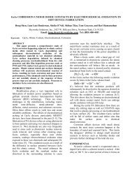
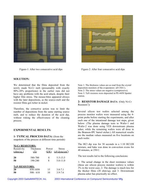
Figure-1: After two consecutive acid dipsFigure-2: After four consecutive acid dipsSOLUTION:We determined that the films deposited from thenewly made <strong>Ni</strong>-<strong>Cr</strong> melt (presumably <strong>with</strong> exactly80%-20% proportions) in the earlier runs did nothave any problems <strong>with</strong> the acid attack, despite theirhigher film stress. The mouse-bites appeared always<strong>with</strong> the later depositions, as the source-melt <strong>and</strong> theresistor films got richer in nickel.Therefore, the corrective action was to limit thenumber of depositions from the same starting sourcemelt, <strong>and</strong> to reduce the duration of the acid dip,<strong>with</strong>out risking the effectiveness of the cleaningprocess.EXPERIMENTAL RESULTS:1- TYPICAL PROCESS DATA: (from thesnapshots of the process at different time periods)<strong>Ni</strong>-<strong>Cr</strong> RESISTORS:Resistivity Thickness Power <strong>Stress</strong>(ohm/sq.) (Å) (kW) (e9 dyne/cm 2 )20 580-700 8 5.5-13.550 190-240 8 5.0-11.0TaN RESISTORS:20 850-1050 15 3.0-7.150 500- 610 10 3.9-7.6Note 1: The thickness values are as read from the crystaldeposition monitors of the evaporators- all CHA’s.Note 2: The stress values are negative (compressive).Note 3: TaN resistors were deposited in PE-4450 Sputterstation.2- RESISTOR DAMAGE DATA (Only <strong>Ni</strong>-<strong>Cr</strong>Resistors 3 ):Several silicon test wafers selected among theprocess monitor wafers were measured using the 4-point probe before starting the experiments, <strong>and</strong> aftereach one of the intentional damage test steps, givenbelow: (The plasma damage tests to Wafer-1 <strong>and</strong>Wafer-2 was done using YES downstream plasmaasher, while the remaining wafers were all done inthe Branson-IPC barrel etcher.) All numerical resultsare the median values measured on five locations oneach wafer.The HCl dip was for 30 seconds in a 1:10 HCl:DImixture, <strong>and</strong> bake was done in convection ovens for40 minutes, at 250 C.The test results led to the following conclusions:1- The actual change in the sheet resistance values(these are silicon process monitor wafers) is <strong>with</strong>in3% in the worst case, 2- The damage is much less forthe thicker films (20 ohm/sq), <strong>and</strong> 3- Downstreamplasma asher has practically no effect.