DLP-HS-FPGA/2 - DLP Design
DLP-HS-FPGA/2 - DLP Design
DLP-HS-FPGA/2 - DLP Design

Create successful ePaper yourself
Turn your PDF publications into a flip-book with our unique Google optimized e-Paper software.
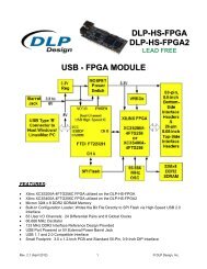
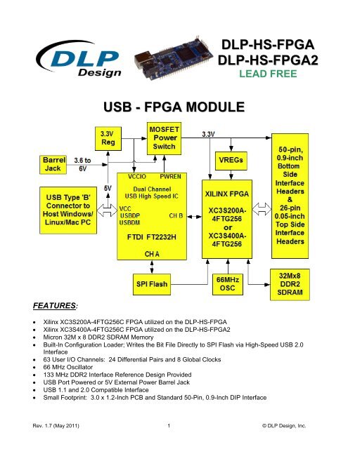
USB - <strong>FPGA</strong> MODULE<strong>DLP</strong>-<strong>HS</strong>-<strong>FPGA</strong><strong>DLP</strong>-<strong>HS</strong>-<strong>FPGA</strong>2LEAD FREEFEATURES:• Xilinx XC3S200A-4FTG256C <strong>FPGA</strong> utilized on the <strong>DLP</strong>-<strong>HS</strong>-<strong>FPGA</strong>• Xilinx XC3S400A-4FTG256C <strong>FPGA</strong> utilized on the <strong>DLP</strong>-<strong>HS</strong>-<strong>FPGA</strong>2• Micron 32M x 8 DDR2 SDRAM Memory• Built-In Configuration Loader; Writes the Bit File Directly to SPI Flash via High-Speed USB 2.0Interface• 63 User I/O Channels: 24 Differential Pairs and 8 Global Clocks• 66 MHz Oscillator• 133 MHz DDR2 Interface Reference <strong>Design</strong> Provided• USB Port Powered or 5V External Power Barrel Jack• USB 1.1 and 2.0 Compatible Interface• Small Footprint: 3.0 x 1.2-Inch PCB and Standard 50-Pin, 0.9-Inch DIP InterfaceRev. 1.7 (May 2011) 1 © <strong>DLP</strong> <strong>Design</strong>, Inc.
APPLICATIONS:• Rapid Prototyping• Educational Tool• Industrial/Process Control• Data Acquisition/Processing• Embedded Processor1.0 INTRODUCTIONThe <strong>DLP</strong>-<strong>HS</strong>-<strong>FPGA</strong> module is a low-cost, compact prototyping tool that can be used for rapid proof ofconcept or within educational environments. The module is based on the Xilinx Spartan 3A andFuture Technology Devices International’s FT2232H Dual-Channel High-Speed USB IC. The<strong>DLP</strong>-<strong>HS</strong>-<strong>FPGA</strong> provides both the beginner as well as the experienced engineer with a rapid path todeveloping <strong>FPGA</strong>-based designs. When combined with the free ISE WebPACK tools from Xilinx,this module is more than sufficient for creating anything from basic logical functions to a highlycomplex system controller.As a bonus feature, one channel of the dual-channel USB interface is used to load user bit filesdirectly to the SPI Flash—no external programmer is required. This represents a savings of as muchas $200 in that no additional programming cable is required for configuring the <strong>FPGA</strong>. All that isneeded to load bit files to the <strong>DLP</strong>-<strong>HS</strong>-<strong>FPGA</strong> is a Windows software utility (free with purchase), aWindows PC and a USB cable. The module can also be programmed from within the Xilinx ISE toolenvironment using a Xilinx programming cable (purchased separately).The <strong>DLP</strong>-<strong>HS</strong>-<strong>FPGA</strong> is fully compatible with the free ISE WebPACK tools from Xilinx. ISEWebPACK offers the ideal development environment for <strong>FPGA</strong> designs with HDL synthesis andsimulation, implementation, device fitting and JTAG programming.The <strong>DLP</strong>-<strong>HS</strong>-<strong>FPGA</strong> has on-board voltage regulators that generate all required power supply voltagesfrom a single 5-volt source. Power for the module can be taken from either the host USB port or froma user-supplied, external 5-volt power supply via an onboard standard barrel connector.Connection to user electronics is made via a 50-pin, 0.9-inch wide, industry-standard 0.025-squareinch post DIP header on the bottom of the board and a 26-pin, 0.05-inch wide top side 2x13 header.The bottom side 50-pin header provides access to 41 of the <strong>FPGA</strong> user input/output pins. The topside header provides access to 22 of the <strong>FPGA</strong> user input/output pins. The bottom side header mateswith a user-supplied, standard, 50-pin, 0.9-inch spaced DIP socket. The top side header mates with aRev. 1.7 (May 2011) 2 © <strong>DLP</strong> <strong>Design</strong>, Inc.
user-supplied, 0.05-inch spaced, 2x13 connector such as the FFSD-13-D-xx.xx-01 (xx.xx = cablelength) ribbon cable assembly from Samtec.DIP SocketRibbon CableOther on-board features include a 32M x 8 DDR2 SDRAM memory IC for user projects and bothJTAG and SPI Flash interface ports for connection to Xilinx programming tools.2.0 REFERENCE DESIGNA 10,000-line reference design is available for the Spartan 3A <strong>FPGA</strong> on the <strong>DLP</strong>-<strong>HS</strong>-<strong>FPGA</strong> to thosewho purchase the module. The design was written in VHDL and built using the free Xilinx ISEWebPACK tools. The reference design consists of the following blocks:It contains a USB Interface Block, a User I/0 Block, a DDR2 SDRAM interface, a Heartbeat PulseGenerator and a Clock Generator. The SPI Flash is used to store the design’s <strong>FPGA</strong> configurationfile.The USB interface captures, interprets and returns command and data information sent from the hostPC through the FTDI USB interface to the <strong>FPGA</strong>. Commands include Ping, Return Status, LoopbackData, Set a User I/O Pin High or Low, Read a User I/O Pin, Initialize the DDR2 SDRAM Memory andRead or Write the DDR2 SDRAM Memory. (Section 11 explains these in detail.)Rev. 1.7 (May 2011) 3 © <strong>DLP</strong> <strong>Design</strong>, Inc.
The User I/O Block controls access to the 63 user I/O pins accessible through the top- and bottomsideheaders. Every one of these pins can be either an input or an output. The User I/O Block canconfigure these pins as inputs and read their state, or as outputs and drive them high or low. (As aside note, 48 of these user I/O pins can be configured as 24 differential pairs, 8 can be configured asglobal clock inputs and 6 can be configured as regional clock inputs.)The DDR2 SDRAM interface block manages the memory’s initialization, the refresh cycle and theread and write access. Read and write access is available in 4-byte bursts. The traces between theDDR2 SDRAM and <strong>FPGA</strong> are matched within 10 mils to accommodate reliable data transfer at 266Mbit/s (clocked at 133MHz). The interface creates and aligns the Data Strobes (DQS) based on anexternal feedback trace that matches two times the trace length between the <strong>FPGA</strong> and the DDR2SDRAM. The Initialization, Read and Write commands are initiated by the USB interface block andexecuted by the DDR2 SDRAM interface block.The Heartbeat Pulse Generator takes the internal system clock and divides it down so that theonboard Heartbeat LED will be turned on and off for a duration of approximately one-half second.The Clock Generator Block receives the 66-MHz clock and produces both the 133-MHz clocksrequired to run the DDR2 SDRAM memory device and the 100-MHz clock for the remaining internallogic in the <strong>FPGA</strong>. It also handles reset and lock synchronization between internal DCM blocks.The design occupies the following <strong>FPGA</strong> resources on the <strong>DLP</strong>-<strong>HS</strong>-<strong>FPGA</strong> module’s XC3S200A:The design occupies the following <strong>FPGA</strong> resources on the <strong>DLP</strong>-<strong>HS</strong>-<strong>FPGA</strong>2 module’s XC3S400A:Rev. 1.7 (May 2011) 4 © <strong>DLP</strong> <strong>Design</strong>, Inc.
More reference designs are planned. Please contact <strong>DLP</strong> <strong>Design</strong> with any specific requests.3.0 <strong>FPGA</strong> SPECIFICATIONSThe <strong>FPGA</strong> device used on the <strong>DLP</strong>-<strong>HS</strong>-<strong>FPGA</strong> is the Xilinx Spartan 3A: XC3S200A-4FTG256• Part Number: XC3S200A-4FTG256C• System Gates: 200,000• Equivalent Logic Cells: 4,032• CLB Array:Rows: 32Columns: 16Total CLB’s: 448Total Slices: 1,792Total Flip Flops: 3,584Total 4-Input LUT’s: 3,584• Distributed RAM Bits: 28K• Block RAM Bits: 288K• Dedicated Multipliers: 16• DCM’s: 4Rev. 1.7 (May 2011) 5 © <strong>DLP</strong> <strong>Design</strong>, Inc.
The <strong>FPGA</strong> device used on the <strong>DLP</strong>-<strong>HS</strong>-<strong>FPGA</strong>2 is the Xilinx Spartan 3A: XC3S400A-4FTG256• Part Number: XC3S400A-4FTG256C• System Gates: 400,000• Equivalent Logic Cells: 8,064• CLB Array:Rows: 40Columns: 24Total CLB’s: 896Total Slices: 3,584Total Flip Flops: 7,168Total 4-Input LUT’s: 7,168• Distributed RAM Bits: 56K• Block RAM Bits: 360K• Dedicated Multipliers: 20• DCM’s: 44.0 ABSOLUTE MAXIMUM RATINGSStresses above those listed here may cause permanent damage to the <strong>DLP</strong>-<strong>HS</strong>-<strong>FPGA</strong>:Operating Temperature: 0-70°CVoltage on Digital Inputs with Respect to Ground: -0.5V to +4.1 VSink/Source Current on Any I/O: 24 mA (using LVTTL as the <strong>FPGA</strong> I/O standard)5.0 WARNINGS• Unplug from the host PC and power adapter before connecting to I/O on the <strong>DLP</strong>-<strong>HS</strong>-<strong>FPGA</strong>.• Isolate the bottom of the board from all conductive surfaces.• Observe static precautions to prevent damage to the <strong>DLP</strong>-<strong>HS</strong>-<strong>FPGA</strong> module.6.0 BITLOADAPP SOFTWAREWindows software is provided for use with the <strong>DLP</strong>-<strong>HS</strong>-<strong>FPGA</strong> that will load an <strong>FPGA</strong> configuration(*.bit) file directly to the SPI Flash device via the USB interface. This application (illustrated below) willallow the user to erase the Flash, verify the erasure and then program and verify the Flash:Rev. 1.7 (May 2011) 6 © <strong>DLP</strong> <strong>Design</strong>, Inc.
7.0 JTAG INTERFACEThe easiest way to load an <strong>FPGA</strong> configuration (*.bit) file to the <strong>FPGA</strong> is to run the BitLoadAppsoftware then select and program a file from the local hard drive directly to the SPI Flash. Oncewritten to the SPI Flash, the configuration will load to the <strong>FPGA</strong> and execute. Alternatively, atraditional JTAG header location is provided on the <strong>DLP</strong>-<strong>HS</strong>-<strong>FPGA</strong> giving the user access to thespecific pins required by the development tools. (Refer to the schematic contained within thisdatasheet for details.)8.0 EEPROM SETUP / MPROGThe <strong>DLP</strong>-<strong>HS</strong>-<strong>FPGA</strong> has a dual-channel USB interface to the host PC. Channel A is used exclusivelyto load an <strong>FPGA</strong> configuration (*.bit) file to the SPI Flash. This configuration data is automaticallytransferred to the <strong>FPGA</strong> when power is applied to the module or when the PROG Pin is driven lowand then released by the application software. Channel B is used for communication between the<strong>FPGA</strong> and host PC at run time. A 93LC56B EEPROM connected to the USB interface IC is used tostore the setup for the two channels. The parameters stored in the EEPROM include the Vendor ID(VID), Product ID (PID), Serial Number, Description String, driver selection (VCP or D2XX) and porttype (UART serial or FIFO parallel).As mentioned above, Channel A is used exclusively for loading the <strong>FPGA</strong>’s configuration to the SPIFlash, and Channel B is used for communication between the host PC and the <strong>DLP</strong>-<strong>HS</strong>-<strong>FPGA</strong>. Assuch, the D2XX drivers and 245 FIFO mode must be selected in the EEPROM for Channel A.Channel B must use the 245 FIFO mode, but it can use either the VCP or D2XX drivers. The VCPdrivers make the <strong>DLP</strong>-<strong>HS</strong>-<strong>FPGA</strong> appear as an RS232 port to the host application. The D2XX driversprovide faster throughput, but require working with a *.lib or *.dll library in the host application.The operational modes and other EEPROM selections are written to the EEPROM using the MPROGutility. This utility and its manual are available for download from the bottom of the page atwww.dlpdesign.com.Rev. 1.7 (May 2011) 7 © <strong>DLP</strong> <strong>Design</strong>, Inc.
9.0 TEST BIT FILEA test file is provided as a download from the <strong>DLP</strong> <strong>Design</strong> website that provides rudimentary accessto the I/O features of the <strong>DLP</strong>-<strong>HS</strong>-<strong>FPGA</strong>. The following features are provided:• Ping• Read the High/Low State of the Input-Only Pins• Drive I/O Pins High/Low or Read their High/Low State• Simple Loopback on Channel B• 4 Byte Read/Write Access of Row, Column, and Bank Address in the DDR2 SDRAMThis bit file is available from the <strong>DLP</strong>-<strong>HS</strong>-<strong>FPGA</strong>’s download page. The command structure thatsupports these features is explained in Section 11.Rev. 1.7 (May 2011) 8 © <strong>DLP</strong> <strong>Design</strong>, Inc.
10.0 USB DRIVERSUSB drivers for the following operating systems are available for download from the <strong>DLP</strong> <strong>Design</strong>website at www.dlpdesign.com:Notes:OPERATING SYSTEM SUPPORTWindows 7 32-bitWindows 7 64-bitWindows Vista, Vista x64Mac OSXWindows XP, XP x64Mac OS9Windows Server 2008, x64Mac OS8Windows Server 2003, x64LinuxWindows 2000 Windows CE 4.2 – 6.01. The bit file load utility only runs on the Windows platforms.2. The bit file load utility requires the use of USB channel A, and channel A is dedicated to thisfunction.3. If you are utilizing the dual-mode drivers from FTDI (CDM2.x.x) and you want to use the VirtualCOM Port (VCP) drivers, then it may be necessary to disable the D2XX drivers first via DeviceManager. To do so, right click on the entry under USB Controllers that appears when the<strong>DLP</strong>-<strong>HS</strong>-<strong>FPGA</strong> is connected, select Properties, select the Advanced tab, check the option for“Load VCP” and click OK. Then unplug and replug the <strong>DLP</strong>-<strong>HS</strong>-<strong>FPGA</strong>, and a COM port shouldappear in Device Manager under Ports (COM & LPT).11.0 USING THE <strong>DLP</strong>-<strong>HS</strong>-<strong>FPGA</strong>Select a power source via Header Pins 23 and 24, and connect the <strong>DLP</strong>-<strong>HS</strong>-<strong>FPGA</strong> to the PC toinitiate the loading of USB drivers. The easiest way to do this is to connect Pins 23 and 24 to eachother. This will result in operational power being taken from the host PC. Once the drivers are loaded,the <strong>DLP</strong>-<strong>HS</strong>-<strong>FPGA</strong> is ready for use.Rev. 1.7 (May 2011) 9 © <strong>DLP</strong> <strong>Design</strong>, Inc.
Simply connect the <strong>DLP</strong>-<strong>HS</strong>-<strong>FPGA</strong> to the PC to initiate the loading of USB drivers. Once the USBdrivers are loaded, the <strong>DLP</strong>-<strong>HS</strong>-<strong>FPGA</strong> is ready for use. All commands are issued as multi-bytecommand packets consisting of at least two bytes.You can either utilize the Test Application available from http://www.dlpdesign.com/test.shtml withthe <strong>DLP</strong>-<strong>HS</strong>-<strong>FPGA</strong> (as described in Section 12), or you can write your own program in your languageof choice.If you are using the VCP drivers, begin by opening the COM port, and send multi-byte commands asshown in Table 1 below. There is no need to set the baud rate because the <strong>DLP</strong>-<strong>HS</strong>-<strong>FPGA</strong> uses aparallel interface between the USB IC and the <strong>FPGA</strong>. (The Ping Command can be used to locate thecorrect COM port used for communicating with the <strong>DLP</strong>-<strong>HS</strong>-<strong>FPGA</strong>, or you can look in DeviceManager to see which port was assigned by Windows.) If you are using the D2XX drivers as with theTest Application, no COM port selection is necessary.TABLE 1Command PacketsCommandPacket Description ByteHexValue Return/CommentsPing Issues Ping 0 0x00 Ping Command - 0x56 will be returned indicating thatthe <strong>DLP</strong>-<strong>HS</strong>-<strong>FPGA</strong> is found on the selected port.ReadVersion/StatusLoopbackLoopbackComplimentRead PinAccessesthe internalversion/statusregistersReturns thedata bytereceivedReturns thecomplimentof data bytereceivedReads thestate of oneof the userI/O pins0 0x10 Read Version/Status Registers Command1 0xnn Register Address: 0xnn =0x00 = Board ID (0x11 = Production PCB)0x01 = <strong>FPGA</strong> Type ID : 0x3A = XC3S200A0x4A = XC3S400A0x02 = <strong>Design</strong> Version ID 1 (<strong>Design</strong> Month)0x03 = <strong>Design</strong> Version ID 2 (<strong>Design</strong> Day)0x04 = <strong>Design</strong> Version ID 3 (<strong>Design</strong> Year)0x05 = <strong>Design</strong> Version ID 4 (<strong>Design</strong> Version)0x06 = DDR2 Status: 0x00 = Not Initialized0x01 = Initialized0 0x20 Loopback Command1 0xnn The byte sent to the <strong>DLP</strong>-<strong>HS</strong>-<strong>FPGA</strong> (0xnn) will bereturned back.0 0x21 Loopback Compliment Command1 0xnn The byte sent to the <strong>DLP</strong>-<strong>HS</strong>-<strong>FPGA</strong> (0xnn) will becomplimented and returned back.0 0x30 Read Pin Command1 0x00–0x3EThe user I/O pin numbers are described in Table 2.User I/O pin 0xnn is read and returns:0x00 = User I/O pin 0xnn is low0x01 = User I/O pin 0xnn is highRev. 1.7 (May 2011) 10 © <strong>DLP</strong> <strong>Design</strong>, Inc.
Clear PinSet PinInitializeMemoryForces theselecteduser I/O pinlowForces theselecteduser I/O pinhighInitializesDDR2SDRAM0 0x40 Clear Pin Command1 0x00–0x3EThe user I/O pin numbers are described in Table 2.User I/O pin 0xnn is cleared. The specified user I/Onumber is returned.0 0x41 Set Pin Command1 0x00–0x3E is returned.The user I/O pin numbers are described in Table 2.User I/O pin 0xnn is set. The specified user I/O number0 0x70 The Initialize Memory Command configures the DDR2SDRAM for access by the <strong>FPGA</strong>. The memory cannotbe accessed without being initialized.Important Note on DDR2 SDRAM Data Access:DDR2 SDRAM data accesses using the reference design on the <strong>DLP</strong>-<strong>HS</strong>-<strong>FPGA</strong> module are alwaysperformed 4 bytes at a time due to the fact that the device is configured for a burst length of four.What this means is that column address Bits 0 and 1 only change the order of the read or write bytes;they still refer to the same 4 bytes. Therefore, to increment the DDR2 SDRAM address forconsecutive memory locations, the column address must be incremented by 4.Incrementing the column address by anything less than 4 simply changes the order in which the 4bytes specified by column address 9:3 are written to the memory or returned to the user. For example,a write to a column starting address of 0 will write to column locations 0, 1, 2 and 3. But if the userthen writes to column address 1, they will actually be writing to column locations 1, 2, 3 and 0, whichwill overwrite the previous write operation.More details on how the DDR2 SDRAM column bits 1 and 0 function can be found in Figure 4 andTable 40 of the Micron MT47H32M8 datasheet. For details on how the bank, row and column bitsare sent via USB to the memory, refer to the commands below:MemoryReadReads 4bytes fromthe DDRSDRAM0 0x8n Reads 4 bytes from the DDR2 SDRAM starting with theaddress specified. The command byte is OR’d with theMost Significant Row Address Bit (24).n = 0 the Most Sig Row Address Bit is low (0x80)n = 1 the Most Sig Row Address Bit is high (0x81)1 0xah Bits 23-16 Middle 8 bits of Row Address to be read from2 0xam Bits 15-12 Lower 4 bits of Row Address to be read fromBits 11-8 Upper 4 bits Column Address to be read from3 0xal Bits 7-2: Lower 6 bits of Column Address to be readfromNOTES: Refer to the text above regarding Column Bits1 and 0 (equates to 0xal bits 3-2). Bits 1-0: BankAddress to be read from.If the memory has not been initialized, the data returnedwill be invalid, and the command returned will be 0xE7indicating the error.Rev. 1.7 (May 2011) 11 © <strong>DLP</strong> <strong>Design</strong>, Inc.
MemoryWriteWrites 4bytes to theDDRSDRAM0 0x9n Writes 4 bytes to the DDR2 SDRAM starting with theaddress specified. The command byte is OR’d with theMost Significant Row Address bit (24).n = 0 the Most Sig Row Address bit is low (0x90)n = 1 the most Sig Row Address bit is high (0x91)1 0xah Bits 23-16 Middle 8 bits of Row Address to be written to2 0xam Bits 15-12 Lower 4 bits of Row Address to be written toBits 11-8 Upper 4 bits Column Address to be written to3 0xal Bits 7-2: Lower 6 bits of column address to be written toNOTE: Refer to the text above regarding Column Bits 1and 0 (equates to 0xal bits 3-2). Bits 1-0: Bank Addressto be written to4 0xd0 Data Byte 0 written to Address Specified5 0xd1 Data Byte 1 written to Address Specified + 16 0xd2 Data Byte 2 written to Address Specified + 27 0xd3 Data Byte 3 written to Address Specified + 3. Returnsthe 4 bytes written followed by an echo back of thecommand and address data sent.NOTE: If the memory has not been initialized, thecommand returned will be 0xE7 indicating the error.The USER I/O Pin Read/Set/Clear Commands I/O number mapping to the physical I/O pins on the<strong>DLP</strong>-<strong>HS</strong>-<strong>FPGA</strong> board are described in the following table:TABLE 2User I/OI/O NumberXC3S200A XC3S200A<strong>DLP</strong>-<strong>HS</strong>-XC3S400A XC3S400A<strong>FPGA</strong> PinPin Bank<strong>FPGA</strong> Pin Configurations Available0x00 (0) J1 Pin 2 D13 0 Digital Input, Output, Differential Pair 0+0x01 (1) J1 Pin 3 C13 0 Digital Input, Output, Differential Pair 0-0x02 (2) J1 Pin 4 D11 0 Digital Input, Output, Differential Pair 1-0x03 (3) J1 Pin 5 C12 0 Digital Input, Output, Differential Pair 1+0x04 (4) J1 Pin 6 C10 0Digital Input, Output, Differential Pair 2+,Global Clock0x05 (5) J1 Pin 7 D9 0Digital Input, Output, Differential Pair 2-,Global Clock0x06 (6) J1 Pin 8 C8 0Digital Input, Output, Differential Pair 3+,0x07 (7) J1 Pin 9 D8 0Global ClockDigital Input, Output, Differential Pair 3-,Global Clock0x08 (8) J1 Pin 10 A14 0 Digital Input, Output, Differential Pair 4+0x09 (9) J1 Pin 12 A13 0 Digital Input, Output, Differential Pair 4-0x0A (10) J1 Pin 13 A6 0 Digital Input, Output, Differential Pair 5+0x0B (11) J1 Pin 14 B6 0 Digital Input, Output, Differential Pair 5-0x0C (12) J1 Pin 15 C11 0 Digital Input, Output, Differential Pair 6+0x0D (13) J1 Pin 16 A11 0 Digital Input, Output, Differential Pair 6-Rev. 1.7 (May 2011) 12 © <strong>DLP</strong> <strong>Design</strong>, Inc.
0x0E (14) J1 Pin 17 B8 0Digital Input, Output, Differential Pair 7-,Global Clock0x0F (15) J1 Pin 18 A8 0Digital Input, Output, Differential Pair 7+,Global Clock0x10 (16) J1 Pin 19 C5 0 Digital Input, Output, Differential Pair 8-0x11 (17) J1 Pin 20 A5 0 Digital Input, Output, Differential Pair 8+0x12 (18) J1 Pin 21 B3 0 Digital Input, Output, Differential Pair 9-0x13 (19) J1 Pin 22 A3 0 Digital Input, Output, Differential Pair 9+0x14 (20) J1 Pin 27 F3 3 Digital Input, Output, Differential Pair 10+0x15 (21) J1 Pin 29 G4 3 Digital Input, Output, Differential Pair 10-0x16 (22) J1 Pin 30 C2 3 Digital Input, Output, Differential Pair 11+0x17 (23) J1 Pin 31 C1 3 Digital Input, Output, Differential Pair 11-0x18 (24) J1 Pin 32 E1 3 Digital Input, Output, Differential Pair 12-0x19 (25) J1 Pin 33 D1 3 Digital Input, Output, Differential Pair 12+0x1A (26) J1 Pin 34 J6 3 Digital Input, Output, Differential Pair 13-0x1B (27) J1 Pin 35 J4 3 Digital Input, Output, Differential Pair 13+0x1C (28) J1 Pin 36 H6 3 Digital Input, Output, Differential Pair 14+0x1D (29) J1 Pin 37 H5 3 Digital Input, Output, Differential Pair 14-0x1E (30) J1 Pin 38 M4 3 Digital Input, Output, Differential Pair 15-0x1F (31) J1 Pin 39 N3 3 Digital Input, Output, Differential Pair 15+0x20 (32) J1 Pin 41 E3 3 Digital Input, Output, Differential Pair 16+0x21 (33) J1 Pin 42 E2 3 Digital Input, Output, Differential Pair 16-0x22 (34) J1 Pin 43 H3 3 Digital Input, Output, Differential Pair 17+0x23 (35) J1 Pin 44 J3 3 Digital Input, Output, Differential Pair 17-0x24 (36) J1 Pin 45 K1 3Digital Input, Output, Differential Pair 18-,0x25 (37) J1 Pin 46 K3 3Regional ClockDigital Input, Output, Differential Pair 18+,Regional Clock0x26 (38) J1 Pin 47 P1 3 Digital Input, Output, Differential Pair 19-0x27 (39) J1 Pin 48 N2 3 Digital Input, Output, Differential Pair 19+0x28 (40) J1 Pin 49 T9 2 Digital Input, Output, Global Clock0x29 (41) J4 Pin 1 B15 0 Digital Input, Output0x2A (42) J4 Pin 3 A12 0 Digital Input, Output0x2B (43) J4 Pin 5 B10 0 Digital Input, Output, Differential Pair 20+0x2C (44) J4 Pin 7 A10 0 Digital Input, Output, Differential Pair 20-0x2D (45) J4 Pin 9 A9 0 Digital Input, Output, Global Clock0x2E (46) J4 Pin 11 N1 3 Digital Input, Output0x2F (47) J4 Pin 13 E7 0 Digital Input, Output0x30 (48) J4 Pin 15 C4 0 Digital Input, Output0x31 (49) J4 Pin 17 C7 0 Digital Input, Output0x32 (50) J4 Pin 19 K4 3 Digital Input, Output0x33 (51) J4 Pin 21 R1 3 Digital Input, Output0x34 (52) J4 Pin 2 A7 0 Digital Input, Output0x35 (53) J4 Pin 4 A4 0 Digital Input, Output, Differential Pair 21+0x36 (54) J4 Pin 6 B4 0 Digital Input, Output, Differential Pair 21-0x37 (55) J4 Pin 8 F1 3 Digital Input, Output, Differential Pair 22+0x38 (56) J4 Pin 10 G1 3 Digital Input, Output, Differential Pair 22-0x39 (57) J4 Pin 12 H1 3 Digital Input, Output, Regional Clock0x3A (58) J4 Pin 14 J1 3 Digital Input, Output, Regional Clock0x3B (59) J4 Pin 16 L1 3 Digital Input, Output0x3C (60) J4 Pin 18 M1 3 Digital Input, OutputRev. 1.7 (May 2011) 13 © <strong>DLP</strong> <strong>Design</strong>, Inc.
0x3D (61) J4 Pin 20 M3 3 Digital Input, Output, Differential Pair 23+0x3E (62) J4 Pin 22 L4 3 Digital Input, Output, Differential Pair 23-SUSPEND J4 Pin 23 R16 1 Force Suspend Mode (when enabled)AWAKE J4 Pin 24 T11 2 Return from Suspend Mode Operation+5V IN J1 Pin 23 - - +5V input to the <strong>DLP</strong>-<strong>HS</strong>-<strong>FPGA</strong>+5V USB J1 Pin 24 - - +5V supplied by host PC USB port+3.3V OUTJ1 Pin 28,- -+3.3V supplied by the onboard <strong>DLP</strong>-<strong>HS</strong>-GNDJ4 Pin 26J1 Pin 1,J1 Pin 11,J1 Pin 25,J1 Pin 26,J1 Pin 40,J1 Pin 50,J4 Pin 25- -<strong>FPGA</strong> regulator after module enumeratedGroundRev. 1.7 (May 2011) 14 © <strong>DLP</strong> <strong>Design</strong>, Inc.
12.0 USING THE <strong>DLP</strong> TEST APPLICATION (OPTIONAL)Users can design their own application interface to send USB commands to the <strong>DLP</strong>-<strong>HS</strong>-<strong>FPGA</strong>module or utilize the test application tool available from <strong>DLP</strong> <strong>Design</strong>. The <strong>DLP</strong> Test Application isavailable in a free version for download from the <strong>DLP</strong> <strong>Design</strong> website atwww.dlpdesign.com/test.shtml. Using this tool, single- and multi-byte commands can be sent to the<strong>DLP</strong>-<strong>HS</strong>-<strong>FPGA</strong> board.Once installed the test application is used as follows:The commands used to interface to the <strong>DLP</strong>-<strong>HS</strong>-<strong>FPGA</strong> are detailed in Section 10 of this datasheet.Rev. 1.7 (May 2011) 15 © <strong>DLP</strong> <strong>Design</strong>, Inc.
13.0 MECHANICAL DIMENSIONS IN INCHES (MM) (PRELIMINARY)Rev. 1.7 (May 2011) 16 © <strong>DLP</strong> <strong>Design</strong>, Inc.
14.0 SCHEMATICSSchematics for the <strong>DLP</strong>-<strong>HS</strong>-<strong>FPGA</strong> are included on the following three pages:Rev. 1.7 (May 2011) 17 © <strong>DLP</strong> <strong>Design</strong>, Inc.
5544332211D DC CB BA ADownloading<strong>FPGA</strong> CodeFor <strong>FPGA</strong> configurationvia SPI only.PRELIMINARY<strong>DLP</strong>-<strong>HS</strong>-<strong>FPGA</strong>Page 1v1.2UPLOAD500 mADC:+3.6 to +6.0V132Bottom side <strong>FPGA</strong> IO (top view)Top side <strong>FPGA</strong> IODNSEEDATAPWREN#EECSP1V8EESKP5V0USER_IO39_DP19USER_IO36_DN18_RCUSER_IO31_DP15USER_IO2_DN1USER_IO33_DN16USER_IO38_DN19USER_IO40_GCUSER_IO3_DP1USER_IO32_DP16USER_IO34_DP17_RCUSER_IO5_DN2_GC USER_IO35_DN17_RCUSER_IO0_DP0USER_IO18_DN9USER_IO13_DN6USER_IO17_DP8USER_IO24_DN12USER_IO23_DN11USER_IO12_DP6USER_IO20_DP10USER_IO26_DN13USER_IO21_DN10USER_IO25_DP12USER_IO37_DP18_RCUSER_IO22_DP11USER_IO11_DN5USER_IO16_DN8USER_IO19_DP9USER_IO15_DP7_GCUSER_IO14_DN7_GCUSER_IO27_DP13USER_IO7_DN3_GCUSER_IO29_DN14USER_IO6_DP3_GCUSER_IO8_DP4USER_IO28_DP14USER_IO9_DN4USER_IO30_DN15USER_IO4_DP2_GCVCCSWUSER_IO1_DN0FTDI_RXFFTDI_D6FTDI_D2FTDI_D3FTDI_TXEFTDI_D7FTDI_D0FTDI_D1FTDI_RDFTDI_SIFTDI_WRFTDI_D5FTDI_D4SPI_MOSISPI_DINSPI_CSO_B<strong>FPGA</strong>_RESETSPI_CLKVPLLVPHYVPLLVPHYPORTVCC5VIN<strong>FPGA</strong>_AWAKE<strong>FPGA</strong>_SUSPENDVCCSWPORTVCC5VINUSER_IO10_DP5USER_IO41 USER_IO52USER_IO42USER_IO43_DP20USER_IO44_DN20USER_IO45_GCUSER_IO46USER_IO47USER_IO48USER_IO49USER_IO50USER_IO51<strong>FPGA</strong>_SUSPENDUSER_IO53_DP21USER_IO54_DN21USER_IO55_DP22USER_IO56_DN22USER_IO57_RCUSER_IO58_RCUSER_IO59USER_IO60USER_IO61_DP23USER_IO62_DN23<strong>FPGA</strong>_AWAKEVCCSWSPI_PROG3V35V03V33V33V33V33V33V33V35V03V35V0CN1CN-USB12345C81.0uF/0603C77.1uFCN2DC BARREL JACK231D4MBR130T1GC2.1uFTP4 SPARE_ACBUS11C1.01C47.1uFR242.2KJP3PROG Disable12C180.1uFR311KJ1CONN PCB 25x287612345109121113151417161820192524232221343332313029282726403938373635504948474645444342418761234510912111315141716182019252423222134333231302928272640393837363550494847464544434241Q2IRLML6402R2724.9KY112MHzFB2240-1018-11 2C5.1uFC48.1uFR310KC3910uF/10VC170.1uFR2810K 5%R42.2KC3.1uFR190U1FT1232HQ51474256862312064371294507101511152535595857555453524816171819212223242627282930323334383940414344454632146496361136036GNDGNDVCCIOVCCIODPEECLKVCCIOVCCIOVCOREVCOREVCOREVPLLVPHYVREGINDMAGNDGNDGNDGNDGNDGNDGNDBCBUS7/PWRSAV#/PWRSAV#/GPIOH7BCBUS6/-/-/GPIOH6BCBUS5/-/-/GPIOH5BCBUS4/RXLED#/SIWUB/GPIOH4BCBUS3/TXLED#/WR#/GPIOH3BCBUS2/RDSTB#/RD#/GPIOH2BCBUS1/WRSTB#/TXE#/GPIOH1BCBUS0/TXDEN/RXF#/GPIOH0ADBUS0/TXD/D0/TCK SKADBUS1/RXD/D1/TDI DOADBUS2/RTS#/D2/TDO DIADBUS3/CTS#/D3/TMS CSADBUS4/DTR#/D4/GPIOL0ADBUS5/DSR#/D5/GPIOL1ADBUS6/DCD#/D6/GPIOL2ADBUS7/RI#/D7/GPIOL3ACBUS0/TXDEN/RXF#/GPIOH0ACBUS1/WRSTB#/TXE#/GPIOH1ACBUS2/RDSTB#/RD#/GPIOH2ACBUS3/TXLED#/WR#/GPIOH3ACBUS4/RXLED#/SIWUA/GPIOH4ACBUS5/-/CLKOUT/GPIOH5ACBUS6/-/OE#/GPIOH6ACBUS7/-/-/GPIOH7BDBUS0/TXD/DO/TCK SKBDBUS1/RXD/D1/TDI DOBDBUS2/RTS#/D2/TDO DIBDBUS3/CTS#/D3/TMS CSBDBUS4/DTR#/D4/GPIOL0BDBUS5/DSR#/D5/GPIOL1BDBUS6/DCD#/D6/GPIOL3BDBUS7/RI#/D7/GPIOL4OSCOOSCIRESET#REFVREGOUTEECSEEDATATESTPWREN#SUSPEND#C33.1uFQ4MMBT3904L312C3410/10 TantFB3240-1018-11 2J4CONN HDR 13x215131113579191723212522242624681012141618201513111357919172321252224262468101214161820FB1240-1018-11 2C4.1uFD5REDC9.1uFC49.1uFR610KR32 0C104.7uFC1127pFU393LC4612348765CSSKDINDOUTVCCNCNC/ORGGNDR16 27TP5 SPARE_ACBUS61C64.7uFR17 27R212KC26.1uFR13150C85.1uFC1910/10 TantR7 10KC254.7uFTP6 SPARE_ACBUS71C46.1uFU2NCP605-3.3V415263VOUTVINSENSEGNDVINENC1227pF
54321A1T1F2K2C3P3E5M5F6R6B7K7G8J8H9K9G10R10B11L11E12M12C14P14G15L15A16T16U5FGNDGNDGNDGNDGNDGNDGNDGNDGNDGNDGNDGNDGNDGNDGNDGNDGNDGNDGNDGNDGNDGNDGNDGNDGNDGNDGNDGNDVCCINTVCCINTVCCINTVCCINTVCCINTVCCINT1V2DDR II parallelterminations1.8V REGULATOR200mA MaximumD D2GNDVCCAUXVCCAUXVCCAUXVCCAUXG7H8K8G9J9K10F5M6E11L12VCCSWC622.2 uF0603C692.2 uF0603C630.1uFC130.1uFC640.01uFC320.01uFC650.1uFC700.1uFC660.01uFC710.01uFC670.1uFC680.01uFDDR2_A12DDR2_A7DDR2_A3DDR2_WEnVTT_0V9DDR2_RFU_A13DDR2_A8DDR2_ODTDDR2_A2VTT_0V91.2V REGULATOR1.5A MaximumDDR2_RFU_BA2 VTT_0V9DDR2_BA174 DDR2_A6C CDDR2_BA083 DDR2_RFU_A15R14DDR2_A492C22DDR2_A110 22 uFXC3S200A_FT256VTT_0V9 101R15DDR2_CKE49.9K 1% DNSTANTCAT25-500JALF 50 Ohm910910678RN2DNSDNSCAT25-500JALF 50 Ohm6678RN1CAT25-500JALF 50 OhmRN3DNS55432154321VTT_0V9DDR2_A9DDR2_RFU_A14DDR2_A5DDR2_A1VTT_0V9DDR2_CASnDDR2_A0DDR2_CSnDDR2_RASnVCCSWC234.7uF0603456U8ST1S03 DFN6VIN_SWVIN_A1INSWINHIBIT2GND FB13OUT3EN BYPASS4U7TPS79318DBVR / SOT23-55L13.3uHC140.01 uF06031V8C152.2 uF0603R1850DNSDDR2_A10Q3IRLML64011V2B 220K 5%BVCCSWC722.2 uF1V8R25 330C750.1uFVCCSWUse Ceramic caps2167U6LP2997 SOIC8AVINPVINVREF5VDDQ VTT8SD#VSENSEGND43C7322 uFC740.1uFVREF_0V9VTT_0V9VCCSWDNSC760.1uFVCCSWJ3Xilinx Parallel Cable HeaderTDITDOTMSTCK1VCCSW42123456Y2ENVDDGNDOUT3FXO-HC735-66.666MHZSPI_MOSISPI_DINSPI_CSO_BSPI_CLKR127CLKINR12C200.1uF0603R30100 5%2.5 mS ramp upC420.1uF0603D2GREENJ2VCCSWR114.7KDNSVCCSW8U5EJTAG_DINJTAG_TMSLEDG_DONEJTAG_DOUTJTAG_TCKSPI_PROGDNSA M25P20AXC3S200A_FT256Traditional JTAGU4VCCSWR21 4.7KDNSDNS123456JTAG_TCKJTAG_DOUTJTAG_DINJTAG_TMSR94.7KVCCSWR84.7KR54.7K526137CSWHOLDSPIFlashPRELIMINARY<strong>DLP</strong>-<strong>HS</strong>-<strong>FPGA</strong>V1.2Page 24VSSVCCB1B2T15B16A15A212TDITMSDONETDOTCKPROG_BJP1PROGR104.7K>Din
5544332211D DC CB BA ASuspend powered by Vccaux (3.3V)Mode 001 = SPI FlashVariant Select =111 (Fast Read0x0B)v1.2Page 3<strong>DLP</strong>-<strong>HS</strong>-<strong>FPGA</strong>PRELIMINARYHEARTBEATDNSDDR2_DQSDDR2_DQSnDDR2_CKnDDR2_CKDDR2_CKDDR2_CKnDDR2_DQSDDR2_DQSnFDBKUSER_IO8_DP4USER_IO3_DP1USER_IO2_DN1USER_IO34_DP17_RCUSER_IO32_DP16USER_IO21_DN10USER_IO33_DN16USER_IO20_DP10USER_IO29_DN14USER_IO9_DN4USER_IO28_DP14DDR2_CKEDDR2_CASnDDR2_RASnDDR2_WEnDDR2_CSnDDR2_BA1DDR2_BA0DDR2_A12DDR2_A11DDR2_A10DDR2_A9DDR2_A8DDR2_A7DDR2_A6DDR2_A5DDR2_A4DDR2_A3DDR2_A2DDR2_A1DDR2_A0DDR2_DQ0DDR2_DQ1DDR2_DQ2DDR2_DQ3DDR2_DQ4DDR2_DQ5DDR2_DQ6DDR2_DQ7DDR2_ODTDDR2_A10DDR2_A11DDR2_A12DDR2_DQ0DDR2_DQ1DDR2_DQ2DDR2_DQ3DDR2_DQ4DDR2_DQ5DDR2_DQ6DDR2_DQ7DDR2_ODTDDR2_WEnDDR2_CASnDDR2_A8DDR2_CSnDDR2_A1DDR2_A2DDR2_A6DDR2_CKEDDR2_A5DDR2_A0DDR2_BA1DDR2_A4DDR2_A7DDR2_A3DDR2_RASnDDR2_BA0DDR2_A9DDR2_RFU_BA2DDR2_RFU_A13DDR2_RFU_A14DDR2_RFU_A15DDR2_RFU_BA0DDR2_RFU_A14VREF_0V9VREF_0V9VREF_0V9VREF_0V9VREF_0V9DDR2_RFU_A15DDR2_RFU_A13VREF_0V9<strong>FPGA</strong>_SUSPENDUSER_IO35_DN17_RCUSER_IO36_DN18_RCUSER_IO37_DP18_RCUSER_IO27_DP13USER_IO26_DN13USER_IO61_DP23USER_IO62_DN23USER_IO39_DP19USER_IO31_DP15USER_IO30_DN15USER_IO38_DN19USER_IO5_DN2_GCUSER_IO4_DP2_GCUSER_IO6_DP3_GCUSER_IO0_DP0USER_IO1_DN0SPI_MOSIDDR2_IDONE<strong>FPGA</strong>_AWAKEDDR2_ERRORCLKIN<strong>FPGA</strong>_RESETDDR2_DVALIDLEDR_HEARTBUSER_IO24_DN12USER_IO25_DP12USER_IO23_DN11USER_IO22_DP11SPI_INITUSER_IO13_DN6USER_IO10_DP5USER_IO12_DP6USER_IO11_DN5USER_IO15_DP7_GCUSER_IO14_DN7_GCUSER_IO17_DP8USER_IO16_DN8SPI_CSO_BUSER_IO7_DN3_GCUSER_IO18_DN9USER_IO19_DP9USER_IO40USER_IO41USER_IO42USER_IO43_DP20USER_IO44_DN20USER_IO45_GCUSER_IO46USER_IO47USER_IO48USER_IO50USER_IO51USER_IO52USER_IO53_DP21USER_IO54_DN21USER_IO55_DP22USER_IO56_DN22USER_IO57_RCUSER_IO58_RCUSER_IO59USER_IO60DDR2_ERRORDDR2_DVALIDDDR2_IDONEUSER_IO49FTDI_D4FDTI_D7FDTI_D2FTDI_D5FDTI_WRFTDI_TXEFDTI_D3FTDI_SIFDTI_D6FTDI_D0FTDI_RXFFTDI_RDFDTI_D1SPI_CLKSPI_DIN1V81V8VCCSWVCCSWVCCSW VCCSWVCCSWVCCSWVCCSWTP1 DDR2_ERROR1C350.01uFD3GREENU5BXC3S200A_FT256R16N13N14R15P15P16N16K11K12M13M14L13K13M15M16L14L16J10J11J12J13K15K14K16J16H10 J15E15H12F11F12C15C16D14E13D15D16G11G12F13E14F14G13F15E16G14H13F16G16H16H15H14H11J14N15SUSPENDIO_L01P_1/HDCIO_L01N_1/LDC2IO_L02P_1/LDC1IO_L02N_1/LDC0IO_L03P_1/A0IO_L03N_1/A1IP_L04P_1IP_L04N_1/VREF_1IO_L05P_1IO_L05N_1/VREF_1IO_L06P_1/A2IO_L06N_1/A3IO_L07P_1/A4IO_L07N_1/A5IO_L08P_1/A6IO_L08N_1/A7IP_L09P_1/VREF_1IP_L09N_1IO_L10P_1/A8IO_L10N_1/A9IO_L11P_1/RHCLK0IO_L11N_1/RHCLK1IO_L12P_1/RHCLK2IO_L12N_1/TRDY1/RHCLK3IP_L13P_1 VCCO_1VCCO_1VCCO_1IP_L25N_1IP_L25P_1/VREF_1IO_L24N_1/A25IO_L24P_1/A24IO_L23N_1/A23IO_L23P_1/A22IO_L22N_1/A21IO_L22P_1/A20IP_L21N_1IP_L21P_1/VREF_1IO_L20N_1/A19IO_L20P_1/A18IO_L19N_1/A17IO_L19P_1/A16IO_L18N_1/A15IO_L18P_1/A14IO_L17N_1/A13IO_L17P_1/A12IO_L16N_1/A11IO_L16P_1/A10IO_L15N_1/RHCLK7IO_L15P_1/IRDY1/RHCLK6IO_L14N_1/RHCLK5IP_L13N_1IO_L14P_1/RHCLK4VCCO_1C540.01uFC590.1uFC520.1uFC280.01uFC310.1uFC570.1uFC370.01uFR26330JP2SUSPEND12VIA UNUSED_K51VIAUNUSED_J11 1R234.7KU5DXC3S200A_FT256C2C1D4D3D1E1E4F4E3E2G6G5F3G4F1G1G3H4H6H5G2H1H3J3H7J7 M2H2D2L6L5M4N3P2R1P1N2K6K5N1M1L4M3L3K4J6J4L2L1K1K3J1J2 J5IO_L01P_3IO_L01N_3IO_L02P_3IO_L02N_3IO_L03P_3IO_L03N_3IP_L04P_3IP_L04N_3/VREF_3IO_L05P_3IO_L05N_3IP_L06P_3IP_L06N_3/VREF_3IO_L07P_3IO_L07N_3IO_L08P_3IO_L08N_3/VREF_3IO_L09P_3IO_L09N_3IO_L10P_3IO_L10N_3IO_L11P_3/LHCLK0IO_L11N_3/LHCLK1IO_L12P_3/LHCLK2IO_L12N_3/IRDY2/LHCLK3IP_L13P_3IP_L13N_3 VCCO_3VCCO_3VCCO_3IP_L25N_3/VREF_3IP_L25P_3IO_L24N_3IO_L24P_3IO_L23N_3IO_L23P_3IO_L22N_3IO_L22P_3IP_L21N_3IP_L21P_3IO_L20N_3IO_L20P_3IO_L19N_3IO_L19P_3IO_L18N_3IO_L18P_3IO_L17N_3IO_L17P_3IO_L16N_3IO_L16P_3/VREF_3IO_L15N_3/LHCLK7IO_L15P_3/TRDY2/LHCLK6IO_L14N_3/LHCLK5IO_L14P_3/LHCLK4 VCCO_3C270.1uFR22100TP2 DDR2_DVALID1U5CXC3S200A_FT256N4P4N5R2T2R3T3L7N6P5M7T4R5T5T6N7P6P7N8R7T7M8P8T8N9P9 R12M9R8R4R14T14M11P13N12R13T13P12T12L10N11P11R11T11P10T10L9M10N10T9R9L8IO_L01P_2/M1IO_L01N_2/M0IP_2/VREF_2IO_L02P_2/M2IO_L02N_2/CSO_BIO_L03P_2/RDWR_BIO_L03N_2/VS2IP_2IO_L04P_2/VS1IO_L04N_2/VS0IP_2/VREF_2IO_L05P_2IO_L05N_2IO_L06P_2/D7IO_L06N_2/D6IO_L07P_2IO_L07N_2IO_L08P_2/D5IO_L08N_2/D4IO_L09P_2/GCLK12IO_L09N_2/GCLK13IP_2/VREF_2IO_L10P_2/GCLK14IO_L10N_2/GCLK15IO_L11P_2/GCLK0IO_L11N_2/GCLK1 VCCO_2VCCO_2VCCO_2VCCO_2IO_L20N_2/CCLKIO_L20P_2/D0/DIN/MISOIP_2/VREF_2IO_L19N_2IO_L19P_2IO_L18N_2/D1IO_L18P_2/D2IO_L17N_2/D3IO_L17P_2/INIT_BIP_2/VREF_2IO_L16N_2IO_L16P_2IO_L15N_2/DOUTIO_L15P_2/AWAKEIO_L14N_2/MOSI/CSI_BIO_L14P_2IP_2/VREF_2IO_L13N_2IO_L13P_2IO_L12N_2/GCLK3IO_L12P_2/GCLK2IP_2C400.01uFC550.1uFC410.01uFC380.01uFC612.2 uF0603C290.01uFC300.1uFC560.01uFC240.1uFR20100TP3 DDR2_IDONE1C502.2 uF0603VIAUNUSED_R31C440.1uFC600.01uFC530.1uFC430.1uFC580.1uFU1MT47H32M8BP-37EC8C2D7D3F3G7F7G8G2G3H2H8H3H7J2F8J8J3J7K2K8K3K7F2E8B7A3E3D1D9B1B9A1E9H9L1A9C1C3B8D2B2A7C9D8C7L2K9J1E7A8E1G1L8L3L7E2F9B3A2DQ0DQ1DQ2DQ3WECASRASCSBA0BA1A10A0A1A2A3CK#A4A5A6A7A8A9A11CKECKDQSVSSVSSDQ4DQ5DQ6DQ7VDDVDDVDDVDDVDDQVDDQVDDQVSSQVSSQVSSQVSSQVDDQVSSQVDDQA12VSSVSSVSSDLDQS#VDDLRFU_BA2RFU_A13RFU_A14RFU_A15VREFODTDMRDSQ#/NUC210.01uFC512.2 uF0603C70.1uFR29 4.7KC360.1uFVIAUNUSED_E10 1C450.1uFU5AXC3S200A_FT256D13C13D12B15B14C12D11A14A13B12A12D10E10C11A11F10B10A10C10D9E9C9A9C8D8 B13B9E8B5D5C4E6B3A3B4A4D6C5A5C6D7F7B6A6E7F8C7A7B8A8F9IO_L01P_0IO_L01N_0IP_0IO_L02P_0/VREF_0IO_L02N_0IO_L03P_0IO_L03N_0IO_L04P_0IO_L04N_0IO_L05P_0IO_L05N_0IO_L06P_0IO_L06N_0/VREF_0IO_L07P_0IO_L07N_0IP_0IO_L08P_0IO_L08N_0IO_L09P_0/GCLK4IO_L09N_0/GCLK5IP_0/VREF_0IO_L10P_0/GCLK6IO_L10N_0/GCLK7IO_L11P_0/GCLK8IO_L11N_0/GCLK9 VCCO_0VCCO_0VCCO_0VCCO_0IO_L20N_0/PUDC_BIO_L20P_0/VREF_0IP_0IO_L19N_0IO_L19P_0IO_L18N_0IO_L18P_0IP_0IO_L17N_0IO_L17P_0IO_L16N_0IO_L16P_0IP_0IO_L15N_0IO_L15P_0IO_L14N_0/VREF_0IO_L14P_0IO_L13N_0IO_L13P_0IO_L12N_0/GCLK11IO_L12P_0/GCLK10IP_0C160.1uF
15.0 DISCLAIMER© <strong>DLP</strong> <strong>Design</strong>, Inc., 2000-2011Neither the whole nor any part of the information contained herein nor the product described in thismanual may be adapted or reproduced in any material or electronic form without the prior writtenconsent of the copyright holder.This product and its documentation are supplied on an as-is basis, and no warranty as to theirsuitability for any particular purpose is either made or implied. <strong>DLP</strong> <strong>Design</strong>, Inc. will not accept anyclaim for damages whatsoever arising as a result of the use or failure of this product. Your statutoryrights are not affected. This product or any variant of it is not intended for use in any medicalappliance, device or system in which the failure of the product might reasonably be expected to resultin personal injury.This document provides preliminary information that may be subject to change without notice.16.0 CONTACT INFORMATION<strong>DLP</strong> <strong>Design</strong>, Inc.1605 Roma LaneAllen, TX 75013Phone: 469-964-8027Fax: 415-901-4859Email Sales: sales@dlpdesign.comEmail Support: support@dlpdesign.comWebsite URL: http://www.dlpdesign.comRev. 1.7 (May 2011) 18 © <strong>DLP</strong> <strong>Design</strong>, Inc.