DLP- USB232R USB-SERIAL UART Module - FTDI
DLP- USB232R USB-SERIAL UART Module - FTDI
DLP- USB232R USB-SERIAL UART Module - FTDI

Create successful ePaper yourself
Turn your PDF publications into a flip-book with our unique Google optimized e-Paper software.
<strong>USB</strong>-<strong>SERIAL</strong> <strong>UART</strong> <strong>Module</strong><br />
<strong>DLP</strong>-<br />
<strong><strong>USB</strong>232R</strong><br />
LEAD-FREE<br />
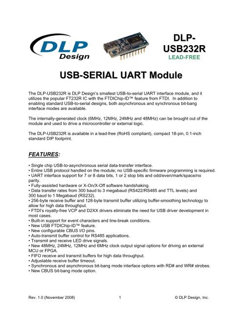
The <strong>DLP</strong>-<strong><strong>USB</strong>232R</strong> is <strong>DLP</strong> Design’s smallest <strong>USB</strong>-to-serial <strong>UART</strong> interface module, and it<br />
utilizes the popular FT232R IC with the <strong>FTDI</strong>Chip-ID feature from <strong>FTDI</strong>. In addition to<br />
enabling standard <strong>USB</strong>-to-serial designs, both asynchronous and synchronous bit-bang<br />
interface modes are available.<br />
The internally-generated clock (6MHz, 12MHz, 24MHz and 48MHz) can be brought out of the<br />
module and used to drive a microcontroller or external logic.<br />
The <strong>DLP</strong>-<strong><strong>USB</strong>232R</strong> is available in a lead-free (RoHS compliant), compact 18-pin, 0.1-inch<br />
standard DIP footprint.<br />
FEATURES:<br />
• Single chip <strong>USB</strong>-to-asynchronous serial data-transfer interface.<br />
• Entire <strong>USB</strong> protocol handled on the module; no <strong>USB</strong>-specific firmware programming is required.<br />
• <strong>UART</strong> interface support for 7 or 8 data bits, 1 or 2 stop bits and odd/even/mark/space/no<br />
parity.<br />
• Fully-assisted hardware or X-On/X-Off software handshaking.<br />
• Data transfer rates from 300 baud to 3 megabaud (RS422/RS485 and TTL levels) and<br />
300 baud to 1 Megabaud (RS232).<br />
• 256-byte receive buffer and 128-byte transmit buffer utilizing buffer-smoothing technology to<br />
allow for high data throughput.<br />
• <strong>FTDI</strong>’s royalty-free VCP and D2XX drivers eliminate the need for <strong>USB</strong> driver development in<br />
most cases.<br />
• Built-in support for event characters and line-break conditions.<br />
• New <strong>USB</strong> <strong>FTDI</strong>Chip-ID feature.<br />
• New configurable CBUS I/O pins.<br />
• Auto-transmit buffer control for RS485 applications.<br />
• Transmit and receive LED drive signals.<br />
• New 48MHz, 24MHz, 12MHz and 6MHz clock output signal options for driving an external<br />
MCU or FPGA.<br />
• FIFO receive and transmit buffers for high data throughput.<br />
• Adjustable receive buffer timeout.<br />
• Synchronous and asynchronous bit-bang mode interface options with RD# and WR# strobes.<br />
• New CBUS bit-bang mode option.<br />
Rev. 1.0 (November 2008) 1 © <strong>DLP</strong> Design, Inc.
• Integrated 1024-bit internal EEPROM for storing <strong>USB</strong> VID, PID, serial number and<br />
product-description strings and CBUS I/O configuration.<br />
• <strong>Module</strong> supplied preprogrammed with unique <strong>USB</strong> serial number.<br />
• Support for <strong>USB</strong> Suspend and Resume.<br />
• Support for bus-powered, self-powered and high-power bus-powered <strong>USB</strong> configurations.<br />
• Integrated level converter on <strong>UART</strong> and CBUS for interfacing to 5V-1.8V logic.<br />
• True 5V/3.3V/2.8V/1.8V CMOS drive output and TTL input.<br />
• High I/O pin output drive option.<br />
• Integrated power-on-reset circuit.<br />
• <strong>UART</strong> signal-inversion option.<br />
• <strong>USB</strong> bulk transfer mode.<br />
• 3.3V to 5.25V single-supply operation.<br />
• Low operating and <strong>USB</strong> Suspend current.<br />
• Low <strong>USB</strong> bandwidth consumption.<br />
• UHCI/OHCI/EHCI host-controller compatible.<br />
• <strong>USB</strong> 2.0 full-speed compatible.<br />
• -40°C to 85°C extended operating temperature range.<br />
• Pb-free and RoHS compliant.<br />
TYPICAL APPLICATIONS:<br />
• <strong>USB</strong> to RS232/RS422/RS485 converters.<br />
• Upgrading legacy peripherals to <strong>USB</strong>.<br />
• Cellular and cordless phone <strong>USB</strong> data-transfer cables and interfaces.<br />
• Interfacing MCU/PLD/FPGA-based designs to <strong>USB</strong>.<br />
• <strong>USB</strong> audio and low-bandwidth video data transfer.<br />
• PDA-to-<strong>USB</strong> data transfer.<br />
• <strong>USB</strong> smart card readers.<br />
• <strong>USB</strong> instrumentation.<br />
• <strong>USB</strong> industrial control.<br />
• <strong>USB</strong> MP3 player interface.<br />
• <strong>USB</strong> FLASH card readers and writers.<br />
• Set top box PC-<strong>USB</strong> interface.<br />
• <strong>USB</strong> hardware modems.<br />
• <strong>USB</strong> wireless modems.<br />
• <strong>USB</strong> bar code readers.<br />
• <strong>USB</strong> software and hardware encryption dongles.<br />
DRIVER SUPPORT:<br />
Royalty-Free Virtual COM Port (VCP) Drivers for:<br />
• Windows 98, 98SE, ME, 2000, Server 2003, XP and Server 2008<br />
• Windows XP and XP 64-bit<br />
• Windows Vista and Vista 64-bit<br />
• Windows XP Embedded<br />
• Windows CE 4.2, 5.0 and 6.0<br />
Rev. 1.0 (November 2008) 2 © <strong>DLP</strong> Design, Inc.
• Mac OS 8/9, OS-X<br />
• Linux 2.4 and greater<br />
Royalty-Free D2XX Direct Drivers (<strong>USB</strong> Drivers + DLL S/W Interface) for:<br />
• Windows 98, 98SE, ME, 2000, Server 2003, XP and Server 2008<br />
• Windows XP and XP 64-bit<br />
• Windows Vista and Vista 64-bit<br />
• Windows XP Embedded<br />
• Windows CE 4.2, 5.0 and 6.0<br />
• Linux 2.4 and greater<br />
Note: The drivers listed above are all available for free download from the <strong>DLP</strong> Design website<br />
www.dlpdesign.com and the <strong>FTDI</strong> website www.ftdichip.com<br />
Various third-party drivers are also available for other operating systems; see the <strong>FTDI</strong> website<br />
www.ftdichip.com for details.<br />
ABSOLUTE MAXIMUM RATINGS<br />
• Storage Temperature<br />
-65°C to +150°C<br />
• Ambient Temperature (Power Applied)<br />
-40°C to +85°C<br />
• VCC Supply Voltage<br />
-0.5V to +6.00V<br />
• DC Input Voltage: High-Impedance Bidirectionals -0.5V to VCC + 0.5V<br />
• DC Output Current: Outputs<br />
24mA<br />
• DC Output Current: Low-Impedance Bidirectionals 24mA<br />
• Electrostatic Discharge Voltage (I
PINOUT DESCRIPTION<br />
Pin 1<br />
Pin 18<br />
<strong>USB</strong><br />
Pin 9<br />
Pin 10<br />
Top View<br />
(Interface Headers on bottom of PCB)<br />
PIN # DESCRIPTION<br />
1 GROUND<br />
2 RTS - Request to Send Control Output/Handshake Signal<br />
3 RI - Ring Indicator Control Input. When remote wake-up is enabled in the internal<br />
EEPROM taking RI# low (20ms active low pulse), this can be used to resume the PC<br />
<strong>USB</strong> host controller from Suspend.<br />
4 DSR - Data Set Ready Control Input/Handshake Signal<br />
5 CTS - Clear To Send Control Input/Handshake Signal<br />
6 CBUS4 - Configurable CBUS output-only pin. The function of this pin is configured in the<br />
FT232R internal EEPROM (see CBUS Signal Options in the next section).<br />
7 VCCIO - +1.8V to +5.25V supply for the <strong>UART</strong> interface and CBUS group (Pins 6, 11,<br />
12, 14 and 15). Connect this pin to an external power supply to drive out at +3.3V levels<br />
(or another voltage within the specified range), or connect to EXTVCC (Pin 8) to drive out<br />
at the +5V CMOS level.<br />
8 EXTVCC - Use for applying main power (4.0 to 5.25 volts) to the module. Connect to<br />
PORTVCC (Pin 9) if the module is to be powered by the <strong>USB</strong> port (typical configuration).<br />
9 PORTVCC - Power from the <strong>USB</strong> port. Connect to EXTVCC (Pin 8) if the module is to<br />
be powered by the <strong>USB</strong> port (typical configuration). 500mA is the maximum current<br />
available to the <strong>USB</strong> adapter and target electronics if the <strong>USB</strong> device is configured for<br />
high power.<br />
10 GROUND<br />
11 CBUS2 - Configurable CBUS I/O pin. The function of this pin is configured in the<br />
FT232R internal EEPROM (see CBUS Signal Options in the next section).<br />
12 CBUS3 - Configurable CBUS I/O Pin. The function of this pin is configured in the<br />
FT232R internal EEPROM (see CBUS Signal Options in the next section).<br />
13 DCD - Data Carrier Detect Control Input<br />
14 CBUS1 - Configurable CBUS I/O Pin. The function of this pin is configured in the<br />
FT232R internal EEPROM (see CBUS Signal Options in the next section).<br />
15 CBUS0 - Configurable CBUS I/O Pin. The function of this pin is configured in the<br />
FT232R internal EEPROM (see CBUS Signal Options in the next section).<br />
16 RXD - Receiving Asynchronous Data Input<br />
17 DTR - Data Terminal Ready Control Output/Handshake Signal<br />
18 TXD - Transmit Asynchronous Data Output<br />
Rev. 1.0 (November 2008) 4 © <strong>DLP</strong> Design, Inc.
CBUS SIGNAL OPTIONS<br />
The following options can be configured on the CBUS I/O pins in the internal EEPROM using<br />
the software utility MPROG, which can be downloaded from www.dlpdesign.com:<br />
CBUS<br />
SIGNAL<br />
OPTION AVAILABLE ON CBUS PIN DESCRIPTION<br />
TXDEN# CBUS0, CBUS1, CBUS2, CBUS3, CBUS4 Enable transmit data for<br />
RS485.<br />
PWREN# CBUS0, CBUS1, CBUS2, CBUS3, CBUS4 This output is low after the<br />
module has been configured<br />
by <strong>USB</strong>, then high<br />
during <strong>USB</strong> Suspend Mode.<br />
This output can be used to<br />
control power to an external<br />
P-channel logic-level<br />
MOSFET switch. Enable<br />
the interface pull-down<br />
option when using the<br />
PWREN# in this way.*<br />
TXLED# CBUS0, CBUS1, CBUS2, CBUS3, CBUS4 Transmit data LED drive;<br />
pulses low when<br />
transmitting data via <strong>USB</strong>.<br />
RXLED# CBUS0, CBUS1, CBUS2, CBUS3, CBUS4 Receive data LED drive;<br />
pulses low when receiving<br />
data.<br />
TX&RXLED# CBUS0, CBUS1, CBUS2, CBUS3, CBUS4 LED drive; pulses low when<br />
transmitting or receiving<br />
data.<br />
SLEEP# CBUS0, CBUS1, CBUS2, CBUS3, CBUS4 Goes low during <strong>USB</strong><br />
Suspend Mode. Typically<br />
used to power down an<br />
external TTL-to-RS232<br />
level converter IC in<br />
<strong>USB</strong>-to-RS232 converter<br />
designs.<br />
CLK48 CBUS0, CBUS1, CBUS2, CBUS3, CBUS4 48MHz clock output**<br />
CLK24 CBUS0, CBUS1, CBUS2, CBUS3, CBUS4 24MHz clock output**<br />
CLK12 CBUS0, CBUS1, CBUS2, CBUS3, CBUS4 12MHz clock output**<br />
CLK6 CBUS0, CBUS1, CBUS2, CBUS3, CBUS4 6MHz clock output**<br />
Rev. 1.0 (November 2008) 5 © <strong>DLP</strong> Design, Inc.
CBitBangI/O CBUS0, CBUS1, CBUS2, CBUS3 CBUS bit-bang mode<br />
option. Allows up to four of<br />
the CBUS pins to be used<br />
as general purpose I/O.<br />
Configured individually for<br />
CBUS0, CBUS1, CBUS2<br />
and CBUS3 in the internal<br />
EEPROM. [A separate<br />
Application Note (AN232R-<br />
01, available from the <strong>FTDI</strong><br />
website (www.ftdichip.com)<br />
describes in more detail<br />
how to use the CBUS<br />
bit-bang mode.]<br />
BitBangWRn CBUS0, CBUS1, CBUS2, CBUS3 Synchronous and<br />
asynchronous bit-bang<br />
mode WR# strobe output.<br />
BitBangRDn CBUS0, CBUS1, CBUS2, CBUS3 Synchronous and<br />
asynchronous bit-bang<br />
mode RD# strobe output.<br />
* PWREN# should be used with a 10k-ohm resistor pull-up.<br />
** When in <strong>USB</strong> Suspend Mode, the output clocks are also suspended.<br />
1.0 QUICK START GUIDE<br />
Note: This guide requires the use of a Windows 98/2000/Vista PC that is equipped with a<br />
<strong>USB</strong> port.<br />
1. Download the CDM drivers from either www.dlpdesign.com or www.ftdichip.com. Unzip<br />
the drivers into a folder on the hard drive.<br />
2. Select a power source for the <strong>DLP</strong>-<strong><strong>USB</strong>232R</strong>. The typical configuration for an all 5-volt<br />
system is to connect Pins 7, 8 and 9.<br />
3. Connect the <strong>DLP</strong>-<strong><strong>USB</strong>232R</strong> module to the host PC via a <strong>USB</strong>-A to Mini-B cable. This action<br />
initiates the loading of <strong>USB</strong> drivers. When prompted, select the folder where the CDM<br />
drivers were stored in Step 1. Windows will then complete the installation of the device<br />
drivers for the <strong>DLP</strong>-<strong><strong>USB</strong>232R</strong> module. The next time the <strong>DLP</strong>-<strong><strong>USB</strong>232R</strong> module is<br />
attached, the host PC will immediately load the correct drivers without any prompting.<br />
Reboot the PC if prompted to do so.<br />
At this point, the <strong>DLP</strong>-<strong><strong>USB</strong>232R</strong> is ready for use.<br />
Rev. 1.0 (November 2008) 6 © <strong>DLP</strong> Design, Inc.
Note: If an extra COM port is not available after installing the CDM drivers, connect the<br />
<strong>DLP</strong>-<strong><strong>USB</strong>232R</strong> and open Control Panel>System>Device Manager. Right click on <strong>USB</strong><br />
Serial Converter under <strong>USB</strong> Controllers and select Properties, then the Advanced tab.<br />
Check the box marked Load VCP, and then click OK. Unplug and re-plug the<br />
<strong>DLP</strong>-<strong><strong>USB</strong>232R</strong>, and a COM port will be added. [This method is also used to convert from<br />
VCP drivers to the D2XX (DLL) drivers.]<br />
2.0 DEVICE CONFIGURATION EXAMPLES<br />
<strong>USB</strong> Bus-Powered and Self-Powered Configurations<br />
Figure 1.<br />
7<br />
8<br />
9<br />
Bus-Powered<br />
5V System<br />
The figure above illustrates a typical <strong>USB</strong> bus-powered configuration. A <strong>USB</strong> bus-powered<br />
device gets its power from the <strong>USB</strong> bus. Basic rules for <strong>USB</strong> bus-powered devices are as<br />
follows:<br />
1. On plug-in to <strong>USB</strong>, the module and external circuitry should draw no more than 100mA on<br />
the 5-volt line from the <strong>USB</strong> host.<br />
2. In <strong>USB</strong> Suspend Mode, the module and external circuitry should draw no more than 2.5mA.<br />
3. A bus-powered, high-power <strong>USB</strong> device (one that draws more than 100mA) should use one<br />
of the CBUS pins configured as PWREN# to keep the current below 100mA on plug-in and<br />
below 2.5mA on <strong>USB</strong> Suspend.<br />
4. A design that consumes more than 100mA in total cannot be plugged into a <strong>USB</strong><br />
bus-powered hub.<br />
5. No <strong>USB</strong> target system can draw more than 500mA from the <strong>USB</strong> bus. The power descriptors<br />
in the internal EEPROM of the FT232R should be programmed to match the total current drawn<br />
by the target system.<br />
Note: If using PWREN# (available using the CBUS), the I/O pin should be pulled to VCCIO<br />
using a 10k-ohm resistor.<br />
Rev. 1.0 (November 2008) 7 © <strong>DLP</strong> Design, Inc.
Figure 2.<br />
5.0V<br />
7<br />
8<br />
9<br />
Self-Powered<br />
5V System<br />
Figure 2 illustrates a typical <strong>USB</strong> self-powered configuration. A <strong>USB</strong> self-powered device gets<br />
its power from its own power supply and does not draw current from the <strong>USB</strong> bus. Basic rules<br />
for <strong>USB</strong> self-powered devices are as follows:<br />
1. A self-powered device should not force current down the <strong>USB</strong> bus when the <strong>USB</strong> host or hub<br />
controller is powered down.<br />
2. A self-powered device can take as much current as it likes during normal operation and<br />
during <strong>USB</strong> Suspend as it has its own power supply.<br />
3. A self-powered device can be used with any <strong>USB</strong> host and both bus- and self-powered <strong>USB</strong><br />
hubs.<br />
Figure 3.<br />
3.3V<br />
Microcontroller<br />
3.3V<br />
7<br />
8<br />
9<br />
TXD<br />
RXD<br />
Bus-Powered<br />
5V System with<br />
3.3 Volt Logic Interface<br />
Figure 3 shows how to configure the <strong>DLP</strong>-<strong><strong>USB</strong>232R</strong> to interface with a 3.3V logic device. In this<br />
example, the target electronics provide the 3.3 volts via the VCCIO line (Pin 7) which, in turn,<br />
will cause the FT232R interface I/O pins to drive out at the 3.3V level.<br />
Rev. 1.0 (November 2008) 8 © <strong>DLP</strong> Design, Inc.
Bus-Powered Circuit with Power Control<br />
<strong>USB</strong> bus-powered circuits need to be able to power down in <strong>USB</strong> Suspend Mode in order to<br />
meet the
3.0 MECHANICAL DRAWING (PRELIMINARY)<br />
INCHES (MILLIMETERS) UNLESS OTHERWISE NOTED<br />
0.21 typ<br />
(5.3 typ)<br />
0.22 typ<br />
(5.6 typ)<br />
Side View<br />
0.23 typ<br />
(5.8 typ)<br />
0.09 typ<br />
(2.3 typ)<br />
0.43 typ<br />
(10.9 typ)<br />
0.37 typ<br />
(9.4 typ)<br />
0.60 typ<br />
(15.2 typ)<br />
1.26 typ<br />
(32.1 typ)<br />
4.0 DISCLAIMER<br />
© <strong>DLP</strong> Design, Inc., 2008<br />
Neither the whole nor any part of the information contained herein nor the product described in<br />
this manual may be adapted or reproduced in any material or electronic form without the prior<br />
written consent of the copyright holder.<br />
This product and its documentation are supplied on an as-is basis, and no warranty as to their<br />
suitability for any particular purpose is either made or implied. <strong>DLP</strong> Design, Inc. will not accept<br />
any claim for damages whatsoever arising as a result of the use or failure of this product. Your<br />
statutory rights are not affected. This product or any variant of it is not intended for use in any<br />
medical appliance, device or system in which the failure of the product might reasonably be<br />
expected to result in personal injury.<br />
Rev. 1.0 (November 2008) 10 © <strong>DLP</strong> Design, Inc.
This document provides preliminary information that may be subject to change without notice.<br />
5.0 CONTACT INFORMATION<br />
<strong>DLP</strong> Design, Inc.<br />
1605 Roma Lane<br />
Allen, TX 75013<br />
Phone: 469-964-8027<br />
Fax: 415-901-4859<br />
Email Sales: sales@dlpdesign.com<br />
Email Support: support@dlpdesign.com<br />
Website URL: http://www.dlpdesign.com<br />
Rev. 1.0 (November 2008) 11 © <strong>DLP</strong> Design, Inc.
5<br />
5<br />
4<br />
4<br />
3<br />
3<br />
2<br />
2<br />
1<br />
1<br />
D D<br />
C C<br />
B B<br />
A A<br />
<strong>DLP</strong> DESIGN<br />
<strong>DLP</strong>-<strong><strong>USB</strong>232R</strong><br />
C3<br />
DCD<br />
DCD<br />
CTS<br />
C1<br />
RI<br />
DTR<br />
TXD<br />
C3<br />
C2<br />
EXTVCC<br />
RTS<br />
RXD<br />
TXD<br />
C1<br />
RI<br />
C4<br />
RXD<br />
DTR<br />
DSR<br />
PORTVCC<br />
C4<br />
RTS<br />
EXTVCC<br />
CTS<br />
C2<br />
VCCIO<br />
C0<br />
DSR<br />
VCCIO<br />
C0<br />
PORTVCC<br />
FB1<br />
240-1018-1<br />
1 2<br />
J1<br />
232 Version<br />
1<br />
2<br />
3<br />
4<br />
5<br />
6<br />
7<br />
8<br />
9<br />
18<br />
17<br />
16<br />
15<br />
14<br />
13<br />
12<br />
11<br />
10<br />
C5<br />
.1uF<br />
C1<br />
10/10 Tant<br />
C4<br />
.47uF<br />
C2<br />
.01<br />
C7<br />
47pF<br />
C3<br />
.1uF<br />
C6<br />
47pF<br />
CN1<br />
<strong>USB</strong> B Conn<br />
1<br />
2<br />
3<br />
4<br />
5<br />
U1 FT232R<br />
1<br />
2<br />
3<br />
4<br />
5<br />
6<br />
7<br />
8<br />
9<br />
10<br />
11<br />
12<br />
13<br />
14<br />
15<br />
16<br />
17<br />
18<br />
19<br />
20<br />
21<br />
22<br />
23<br />
24<br />
25<br />
26<br />
27<br />
28<br />
TXD<br />
DTR#<br />
RTS#<br />
VCCIO<br />
RXD<br />
RI#<br />
GND<br />
VCCIN/NC<br />
DSR#<br />
DCD#<br />
CTS#<br />
CBUS4<br />
CBUS2<br />
CBUS3<br />
<strong>USB</strong>DP<br />
<strong>USB</strong>DM<br />
3V3OUT<br />
GND<br />
RESET#<br />
VCC5 IN<br />
GND<br />
CBUS1<br />
CBUS0<br />
AVCC/NC<br />
AGND<br />
TEST<br />
OSCI<br />
OSCO