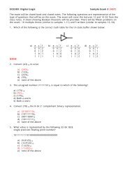
ECE383: Microprocessors â Lab 7 Analog-to-Digital and Digital-to ...
ECE383: Microprocessors â Lab 7 Analog-to-Digital and Digital-to ...
ECE383: Microprocessors â Lab 7 Analog-to-Digital and Digital-to ...

Create successful ePaper yourself
Turn your PDF publications into a flip-book with our unique Google optimized e-Paper software.
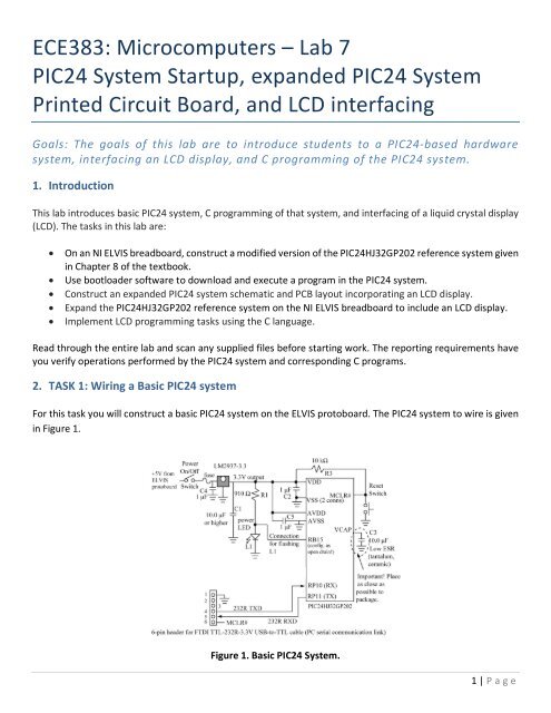
<strong>ECE383</strong>: Microcomputers – <strong>Lab</strong> 7PIC24 System Startup, exp<strong>and</strong>ed PIC24 SystemPrinted Circuit Board, <strong>and</strong> LCD interfacingGoals: The goals of this lab are <strong>to</strong> introduce students <strong>to</strong> a PIC24-based hardwaresystem, interfacing an LCD display, <strong>and</strong> C programming of the PIC24 system.1. IntroductionThis lab introduces basic PIC24 system, C programming of that system, <strong>and</strong> interfacing of a liquid crystal display(LCD). The tasks in this lab are:• On an NI ELVIS breadboard, construct a modified version of the PIC24HJ32GP202 reference system givenin Chapter 8 of the textbook.• Use bootloader software <strong>to</strong> download <strong>and</strong> execute a program in the PIC24 system.• Construct an exp<strong>and</strong>ed PIC24 system schematic <strong>and</strong> PCB layout incorporating an LCD display.• Exp<strong>and</strong> the PIC24HJ32GP202 reference system on the NI ELVIS breadboard <strong>to</strong> include an LCD display.• Implement LCD programming tasks using the C language.Read through the entire lab <strong>and</strong> scan any supplied files before starting work. The reporting requirements haveyou verify operations performed by the PIC24 system <strong>and</strong> corresponding C programs.2. TASK 1: Wiring a Basic PIC24 systemFor this task you will construct a basic PIC24 system on the ELVIS pro<strong>to</strong>board. The PIC24 system <strong>to</strong> wire is givenin Figure 1.Figure 1. Basic PIC24 System.1 | P age
• Wire the PIC24 system according <strong>to</strong> the diagram given in Figure 1.o Use wiring guidelines given in lab 1 for this circuit.o Consult datasheets for any components you might have questions about.o The 3.3V output from the LM2937-3.3 voltage regula<strong>to</strong>r should be attached <strong>to</strong> all power rails onthe ELVIS pro<strong>to</strong>board.o The GND connection on the ELVIS pro<strong>to</strong>board should be attached <strong>to</strong> all the GND rails on the ELVISpro<strong>to</strong>board.o The TA will provide you with a PIC24 programmed with the bootloader software.• Show your wired breadboard <strong>to</strong> the TA. Do not apply power <strong>to</strong> it before the TA has checked it.• Remove the PIC24 from the board before applying power <strong>to</strong> the ELVIS pro<strong>to</strong>board. Turn on the powerswitch <strong>to</strong> the ELVIS unit <strong>and</strong> the ELVIS pro<strong>to</strong>board. Your power LED should come on.• Configure the ELVIS multimeter <strong>to</strong> measure voltage. Use the multimeter <strong>to</strong> verify that the breadboardpower rails have approximately 3.3 V.TA check: Show the TA the wired PIC24 system <strong>and</strong> the measurement of voltage on all ELVIS pro<strong>to</strong>boardpower rails.3. TASK 2: Downloading a Program with the Bootloader• Plug your PIC24 back in<strong>to</strong> the board. Ensure that you have your USB-<strong>to</strong>-Serial cable plugged in<strong>to</strong> theboard <strong>and</strong> in<strong>to</strong> your PC.• Start up the Bully Bootloader on your PC. Select the COM port for USB-To-Serial cable. If you do not knowthe COM port number, then use the ‘Device Manager’ under Control Panel->System->Hardware->DeviceManager <strong>to</strong> see a list of serial ports. Click on a serial port, <strong>and</strong> will see a description of the PORT – theUSB-<strong>to</strong>-Serial manufacturer should be labeled as ‘FTDI’ with location ‘on USB Serial Converter’. Selectthe 57600 baud rate in the bootloader window, <strong>and</strong> click the ‘Open Port’ checkbox <strong>to</strong> open the port.• Copy the chap8 files from the text library <strong>to</strong> a suitable direc<strong>to</strong>ry on your PC hard disk.• Start MPLAB. Open the project echo.mcp (note: you must start MPLAB first, then open the project file –do not open the project file by double-clicking on it since it does not have a workspace file with it).• Compile the echo.mcp project. This project reads a character from the serial port, increments it, <strong>and</strong>echoes it back (so ‘1’ is echoed as ‘2’, ‘a’ as ‘b’, etc.). Use the HexFile but<strong>to</strong>n in the bootloader <strong>to</strong> browse<strong>to</strong> the echo.hex file produced during compilation. Click on the ‘MCLR# <strong>and</strong> Prgrm’ but<strong>to</strong>n in thebootloader <strong>to</strong> download the program in<strong>to</strong> your PIC24 μC (you should see some text appear in the lowerwindow indicating that the program is downloading).• Test the echo.c program functionality by using the ‘Send’ but<strong>to</strong>n <strong>to</strong> send some text <strong>to</strong> the PIC24 μC. Youshould see it echoed back, with the characters incremented by 1.• Modify the echo.c program <strong>to</strong> increment the character by 2 instead of by 1. Verify this operation <strong>and</strong>capture a screenshot of its execution.TA check: Show the TA the operation of the modified echo.c program. Use a screen capture <strong>to</strong>ol <strong>to</strong> captureoutput windows <strong>and</strong> include them in your lab report. Include your source language programs in your labreport.2 | P age
4. TASK 3: Exp<strong>and</strong>ed PIC24 System with LCD DisplayUsing PCB Artist, create an exp<strong>and</strong>ed PIC24 system as shown in Figure 2 below. You may use your schematicfrom the previous lab as a starting point for this design. For this task you will incorporate an LCD interface (4-bitmode) <strong>to</strong> the basic PIC24 system. The LCD module used in this lab is HDM16216L-5 from Hantronix. It allowscharacter output in 2 lines with 16 characters per line. This LCD supports both 4-bit <strong>and</strong> 8-bit interfaces. Thedatasheet for this LCD module can be found here: http://www.hantronix.com/down/16216l5.pdf.The LCD interface is divided in<strong>to</strong> control lines (E, R/W#, RS), data lines (D7:D0) <strong>and</strong> power (VDD, VSS, VL, K, A).The 4-bit interface mode used in this lab is used <strong>to</strong> reduce the number of connections between the PIC24 <strong>and</strong>LCD module, allowing 4 transfer lines <strong>to</strong> be used (D7:D4) <strong>and</strong> the rest (D3:D0) <strong>to</strong> be unused. Figure 2 shows aPIC24 <strong>to</strong> LCD interface for a HDM16216L-5 using the HD44780 LCD controller. Additional description can befound in Chapter 8 of the textbook (pages 302-306). The HDM16216L-5 component is located in the ece383 PCBArtist library on the class website.Figure 2. Exp<strong>and</strong>ed PIC24 System Schematic.3 | P age
The LCD display requires pullup resis<strong>to</strong>rs (R3a-R3g in Figure 2) on the data <strong>and</strong> control lines <strong>to</strong> operate properly.Use the RA8C component from the discrete library for this component. This component will correspond <strong>to</strong> aneight resis<strong>to</strong>r pack in a single inline pin (SIP) package available in the lab. We will only be using seven of the eightavailable resis<strong>to</strong>rs in the component.TA check: Show the TA the schematic design. Use a screen capture <strong>to</strong>ol <strong>to</strong> capture the schematic window <strong>and</strong>include it in your lab report. An example screenshot is given below.5. TASK 4: PIC24 System Printed Circuit Board LayoutFor this task we will create a printed circuit board layout from the PIC24 schematic created as a part of task 3.The board size should be 100mm x 80mm. The board part number should be “<strong>ECE383</strong>-LAB7” <strong>and</strong> the RevisionNumber should be “001”. These parameters can be set through the PCB wizard. Use your experience fromprevious labs <strong>to</strong> create a PCB similar <strong>to</strong> the diagram shown in Figure 3 below.Figure 3. PIC24 System Printed Circuit Board.TA check: Show the TA the printed circuit board you completed. Include a prin<strong>to</strong>ut of your PCB in your labreport.4 | P age
6. TASK 5: Interfacing the LCD Display <strong>to</strong> the PIC24 SystemFor this task you will interface an LCD display (4-bit mode) <strong>to</strong> the PIC24 system constructed in task 1. The LCDrequires a 5V power supply (<strong>to</strong> be provided by the NI ELVIS), <strong>and</strong> therefore needs special consideration in wiring<strong>to</strong> the Microstick operating at 3.3V. Logic voltage level translation can be accomplished by using the open drainconfiguration <strong>and</strong> pull-up resis<strong>to</strong>rs. In addition, all “digital only” pins on PIC24 are 5V <strong>to</strong>lerant. Wire the LCD asfollows:• Wire all data connections as shown in Figure 2:o Pins RB[5:8] on the PIC24 should be connected <strong>to</strong> D[4:7] on the LCD module (U3 on theschematic) leaving D[0:3] on the LCD module unconnected.o Lines D[4:7] should also be pulled up <strong>to</strong> +5V using a resis<strong>to</strong>r bank. Pin 1 on the resis<strong>to</strong>r bank isdesignated with a black dot on the component. All resis<strong>to</strong>rs are connected internally <strong>to</strong> pin 1.Remaining pins on the resis<strong>to</strong>r pack represent the remaining terminal for all resis<strong>to</strong>rs in thecomponent.o VBB (Vss) on the LCD module should be connected <strong>to</strong> ground (GND).o VDD on the LCD module should be connected <strong>to</strong> 5V (from NI ELVIS).o The VDD – VL voltage difference determines the intensity of the characters displayed on the LCD.VL can be connected <strong>to</strong> the wiper terminal of a thumbwheel potentiometer, with another leadon the potentiometer connected <strong>to</strong> the VDD node <strong>and</strong> the other connected <strong>to</strong> ground. In oursetup, we will connect VL <strong>to</strong> ground for maximum intensity.TA check: Show the TA the LCD interfaced <strong>to</strong> the PIC24. Include a picture (from a cell phone) of the LCDinterfaced <strong>to</strong> the PIC24 in the report.7. TASK 6: Character String Output <strong>to</strong> LCDFor this task we will use <strong>and</strong> modify the lcd4bit.mcp project.• Copy the chap8 files <strong>to</strong> a suitable direc<strong>to</strong>ry on your PC hard disk.• Start MPLAB. Open the project lcd4bit.mcp.• Modify the lcd4bit.c code <strong>to</strong> use open drain configuration for all pins connected <strong>to</strong> the LCD <strong>and</strong>configured as outputs (data lines, R/W, etc).• Using “lcd4bit.c” as a starting point, create a program that is capable of displaying your first <strong>and</strong> lastname on the LCD screen as well as your email address.o Write a function that displays your first <strong>and</strong> last name on the <strong>to</strong>p line of the LCD, moves thecursors <strong>to</strong> the bot<strong>to</strong>m line (1 st position) of the LCD, then writes your email address on the bot<strong>to</strong>mline of the LCD.o The characters should scroll across the display (moving right <strong>to</strong> left) at a rate of 200 ms.• Compile <strong>and</strong> download the program <strong>to</strong> the PIC24 system as in Task 2.TA check: Show the TA the operation of the program. Include your source language programs in your labreport. Include a picture (from a cell phone) of the LCD displaying your name.5 | P age
8. TASK 7: Counter Output <strong>to</strong> LCDFor this task, you will implement a counter with a visual output <strong>to</strong> the LCD.• Using the project lcd4bit.mcp as a basis, create a new project named counter_LCD.mcp.• For this task, you will create a program (counter_LCD.c) that will output an incremental counter <strong>to</strong> theLCD screen as follows:o Upon initialization of the program, output a character string “000” <strong>to</strong> the LCD screen.o When SW2 is pressed <strong>and</strong> released, the number on the LCD screen should increment by 1.o Once program counts <strong>to</strong> “20”, the number of the LCD screen should change back <strong>to</strong> “000” <strong>and</strong>begin incrementing again on the press <strong>and</strong> release of SW2.• An interrupt service routine should be programmed <strong>to</strong> h<strong>and</strong>le the state changes of the pushbut<strong>to</strong>n.Code from the project but<strong>to</strong>n_semaphore.mcp in the chap9 direc<strong>to</strong>ry should be useful.TA check: Show the TA the operation of the counter_LCD.c program. Include your source language programin your lab report. Include a picture (from a cell phone) of the LCD displaying your counter values (one picturewill suffice).9. <strong>Lab</strong>ora<strong>to</strong>ry ReportNo later than a week from the day the lab is performed, provide the TA a printed copy of the lab report followingthe <strong>ECE383</strong> <strong>Lab</strong> report Template given on the class website. Each lab group will submit one joint lab report <strong>to</strong>the TA. Your report should have the reporting requirements needed for Tasks 1-7. The TA will take off asignificant number of points (15 points from <strong>to</strong>tal lab grade) if your C source does not have the requiredcomments.10. GRADING POLICY1. Completion of Task 1 with results included in lab report (15%)2. Completion of Task 2 with results included in lab report (10%)3. Completion of Task 3 with results included in lab report (10%)4. Completion of Task 4 with results included in lab report (10%)5. Completion of Task 5 with results included in lab report (15%)6. Completion of Task 6 with results included in lab report (15%)7. Completion of Task 7 with results included in lab report (15%)8. Completeness, quality, <strong>and</strong> correctness of the lab report (10%)6 | P age