ATmega128(L) Preliminary - AVRcard
ATmega128(L) Preliminary - AVRcard
ATmega128(L) Preliminary - AVRcard
- No tags were found...

You also want an ePaper? Increase the reach of your titles
YUMPU automatically turns print PDFs into web optimized ePapers that Google loves.
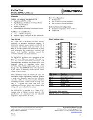
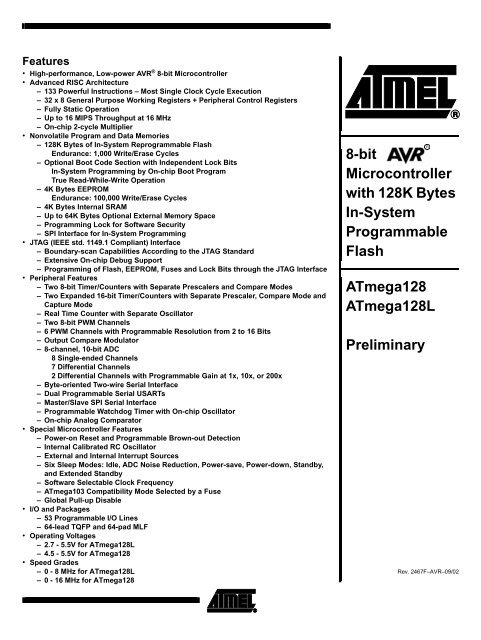
Features• High-performance, Low-power AVR ® 8-bit Microcontroller• Advanced RISC Architecture– 133 Powerful Instructions – Most Single Clock Cycle Execution– 32 x 8 General Purpose Working Registers + Peripheral Control Registers– Fully Static Operation– Up to 16 MIPS Throughput at 16 MHz– On-chip 2-cycle Multiplier• Nonvolatile Program and Data Memories– 128K Bytes of In-System Reprogrammable FlashEndurance: 1,000 Write/Erase Cycles– Optional Boot Code Section with Independent Lock BitsIn-System Programming by On-chip Boot ProgramTrue Read-While-Write Operation– 4K Bytes EEPROMEndurance: 100,000 Write/Erase Cycles– 4K Bytes Internal SRAM– Up to 64K Bytes Optional External Memory Space– Programming Lock for Software Security– SPI Interface for In-System Programming• JTAG (IEEE std. 1149.1 Compliant) Interface– Boundary-scan Capabilities According to the JTAG Standard– Extensive On-chip Debug Support– Programming of Flash, EEPROM, Fuses and Lock Bits through the JTAG Interface• Peripheral Features– Two 8-bit Timer/Counters with Separate Prescalers and Compare Modes– Two Expanded 16-bit Timer/Counters with Separate Prescaler, Compare Mode andCapture Mode– Real Time Counter with Separate Oscillator– Two 8-bit PWM Channels– 6 PWM Channels with Programmable Resolution from 2 to 16 Bits– Output Compare Modulator– 8-channel, 10-bit ADC8 Single-ended Channels7 Differential Channels2 Differential Channels with Programmable Gain at 1x, 10x, or 200x– Byte-oriented Two-wire Serial Interface– Dual Programmable Serial USARTs– Master/Slave SPI Serial Interface– Programmable Watchdog Timer with On-chip Oscillator– On-chip Analog Comparator• Special Microcontroller Features– Power-on Reset and Programmable Brown-out Detection– Internal Calibrated RC Oscillator– External and Internal Interrupt Sources– Six Sleep Modes: Idle, ADC Noise Reduction, Power-save, Power-down, Standby,and Extended Standby– Software Selectable Clock Frequency– ATmega103 Compatibility Mode Selected by a Fuse– Global Pull-up Disable• I/O and Packages– 53 Programmable I/O Lines– 64-lead TQFP and 64-pad MLF• Operating Voltages– 2.7 - 5.5V for <strong>ATmega128</strong>L– 4.5 - 5.5V for <strong>ATmega128</strong>• Speed Grades– 0 - 8 MHz for <strong>ATmega128</strong>L– 0 - 16 MHz for <strong>ATmega128</strong>8-bitMicrocontrollerwith 128K BytesIn-SystemProgrammableFlash<strong>ATmega128</strong><strong>ATmega128</strong>L<strong>Preliminary</strong>Rev. 2467F–AVR–09/021
Pin ConfigurationsFigure 1. Pinout <strong>ATmega128</strong>PENRXD0/(PDI) PE0(TXD0/PDO) PE1(XCK0/AIN0) PE2(OC3A/AIN1) PE3(OC3B/INT4) PE4(OC3C/INT5) PE5(T3/INT6) PE6(IC3/INT7) PE7(SS) PB0(SCK) PB1(MOSI) PB2(MISO) PB3(OC0) PB4(OC1A) PB5(OC1B) PB612345678910111213141516646362616059585756555453525150491718192021222324252627282930313248474645444342414039383736353433PA3 (AD3)PA4 (AD4)PA5 (AD5)PA6 (AD6)PA7 (AD7)PG2(ALE)PC7 (A15)PC6 (A14)PC5 (A13)PC4 (A12)PC3 (A11)PC2 (A10)PC1 (A9)PC0 (A8)PG1(RD)PG0(WR)(OC2/OC1C) PB7TOSC2/PG3TOSC1/1PG4RESETVCCGNDXTAL2XTAL1(SCL/INT0) PD0(SDA/INT1) PD1(RXD1/INT2) PD2(TXD1/INT3) PD3(IC1) PD4(XCK1) PD5(T1) PD6(T2) PD7AVCCGNDAREFPF0 (ADC0)PF1 (ADC1)PF2 (ADC2)PF3 (ADC3)PF4 (ADC4/TCK)PF5 (ADC5/TMS)PF6 (ADC6/TDO)PF7 (ADC7/TDI)GNDVCCPA0 (AD0)PA1 (AD1)PA2 (AD2)OverviewThe <strong>ATmega128</strong> is a low-power CMOS 8-bit microcontroller based on the AVRenhanced RISC architecture. By executing powerful instructions in a single clock cycle,the <strong>ATmega128</strong> achieves throughputs approaching 1 MIPS per MHz allowing the systemdesigner to optimize power consumption versus processing speed.2 <strong>ATmega128</strong>(L)2467F–AVR–09/02
-<strong>ATmega128</strong>(L)Block DiagramFigure 2. Block DiagramPF0 - PF7PA0 - PA7PC0 - PC7XTAL1XTAL2RESETVCCGNDPORTF DRIVERSPORTA DRIVERSPORTC DRIVERSDATA REGISTERPORTFDATA DIR.REG. PORTFDATA REGISTERPORTADATA DIR.REG. PORTADATA REGISTERPORTCDATA DIR.REG. PORTC8-BIT DATA BUSAVCCAGNDAREFADCINTERNALOSCILLATORCALIB. OSCOSCILLATORJTAG TAPPROGRAMCOUNTERSTACKPOINTERWATCHDOGTIMEROSCILLATORON-CHIP DEBUGPROGRAMFLASHSRAMMCU CONTROLREGISTERTIMING ANDCONTROLBOUNDARY-SCANINSTRUCTIONREGISTERGENERALPURPOSEREGISTERSTIMER/COUNTERSPENPROGRAMMINGLOGICINSTRUCTIONDECODERXYZINTERRUPTUNITCONTROLLINESALUEEPROMSTATUSREGISTERUSART0SPIUSART1TWO-WIRE SERIALINTERFACEANALOGCOMPARATOR+DATA REGISTERPORTEDATA DIR.REG. PORTEDATA REGISTERPORTBDATA DIR.REG. PORTBDATA REGISTERPORTDDATA DIR.REG. PORTDDATA REG.PORTGDATA DIR.REG. PORTGPORTE DRIVERSPORTB DRIVERSPORTD DRIVERSPORTG DRIVERSPE0 - PE7PB0 - PB7PD0 - PD7PG0 - PG42467F–AVR–09/023
The AVR core combines a rich instruction set with 32 general purpose working registers.All the 32 registers are directly connected to the Arithmetic Logic Unit (ALU), allowingtwo independent registers to be accessed in one single instruction executed in one clockcycle. The resulting architecture is more code efficient while achieving throughputs up toten times faster than conventional CISC microcontrollers.The <strong>ATmega128</strong> provides the following features: 128K bytes of In-System ProgrammableFlash with Read-While-Write capabilities, 4K bytes EEPROM, 4K bytes SRAM, 53general purpose I/O lines, 32 general purpose working registers, Real Time Counter(RTC), four flexible Timer/Counters with compare modes and PWM, 2 USARTs, a byteoriented Two-wire Serial Interface, an 8-channel, 10-bit ADC with optional differentialinput stage with programmable gain, programmable Watchdog Timer with Internal Oscillator,an SPI serial port, IEEE std. 1149.1 compliant JTAG test interface, also used foraccessing the On-chip Debug system and programming and six software selectablepower saving modes. The Idle mode stops the CPU while allowing the SRAM,Timer/Counters, SPI port, and interrupt system to continue functioning. The Powerdownmode saves the register contents but freezes the OscillatorOscillator, disabling allother chip functions until the next interrupt or Hardware Reset. In Power-save mode, theasynchronous timer continues to run, allowing the user to maintain a timer base whilethe rest of the device is sleeping. The ADC Noise Reduction mode stops the CPU andall I/O modules except Asynchronous Timer and ADC, to minimize switching noise duringADC conversions. In Standby mode, the Crystal/Resonator Oscillator is runningwhile the rest of the device is sleeping. This allows very fast start-up combined with lowpower consumption. In Extended Standby mode, both the main Oscillator and the AsynchronousTimer continue to run.The device is manufactured using Atmel’s high-density nonvolatile memory technology.The On-chip ISP Flash allows the program memory to be reprogrammed in-systemthrough an SPI serial interface, by a conventional nonvolatile memory programmer, orby an On-chip Boot program running on the AVR core. The boot program can use anyinterface to download the application program in the application Flash memory. Softwarein the Boot Flash section will continue to run while the Application Flash section isupdated, providing true Read-While-Write operation. By combining an 8-bit RISC CPUwith In-System Self-Programmable Flash on a monolithic chip, the Atmel <strong>ATmega128</strong> isa powerful microcontroller that provides a highly flexible and cost effective solution tomany embedded control applications.The <strong>ATmega128</strong> AVR is supported with a full suite of program and system developmenttools including: C compilers, macro assemblers, program debugger/simulators, in-circuitemulators, and evaluation kits.ATmega103 and<strong>ATmega128</strong>CompatibilityThe <strong>ATmega128</strong> is a highly complex microcontroller where the number of I/O locationssupersedes the 64 I/O locations reserved in the AVR instruction set. To ensure backwardcompatibility with the ATmega103, all I/O locations present in ATmega103 havethe same location in <strong>ATmega128</strong>. Most additional I/O locations are added in anExtended I/O space starting from $60 to $FF, (i.e., in the ATmega103 internal RAMspace). These locations can be reached by using LD/LDS/LDD and ST/STS/STDinstructions only, not by using IN and OUT instructions. The relocation of the internalRAM space may still be a problem for ATmega103 users. Also, the increased number ofinterrupt vectors might be a problem if the code uses absolute addresses. To solvethese problems, an ATmega103 compatibility mode can be selected by programmingthe fuse M103C. In this mode, none of the functions in the Extended I/O space are inuse, so the internal RAM is located as in ATmega103. Also, the Extended Interrupt vectorsare removed.4 <strong>ATmega128</strong>(L)2467F–AVR–09/02
<strong>ATmega128</strong>(L)The <strong>ATmega128</strong> is 100% pin compatible with ATmega103, and can replace theATmega103 on current Printed Circuit Boards. The application note “ReplacingATmega103 by <strong>ATmega128</strong>” describes what the user should be aware of replacing theATmega103 by an <strong>ATmega128</strong>.ATmega103 CompatibilityModeBy programming the M103C fuse, the <strong>ATmega128</strong> will be compatible with theATmega103 regards to RAM, I/O pins and interrupt vectors as described above. However,some new features in <strong>ATmega128</strong> are not available in this compatibility mode,these features are listed below:• One USART instead of two, Asynchronous mode only. Only the eight leastsignificant bits of the Baud Rate Register is available.• One 16 bits Timer/Counter with two compare registers instead of two 16-bitTimer/Counters with three compare registers.• Two-wire serial interface is not supported.• Port C is output only.• Port G serves alternate functions only (not a general I/O port).• Port F serves as digital input only in addition to analog input to the ADC.• Boot Loader capabilities is not supported.• It is not possible to adjust the frequency of the internal calibrated RC Oscillator.• The External Memory Interface can not release any Address pins for general I/O,neither configure different wait-states to different External Memory Addresssections.In addition, there are some other minor differences to make it more compatible toATmega103:• Only EXTRF and PORF exists in MCUCSR.• Timed sequence not required for Watchdog Time-out change.• External Interrupt pins 3 - 0 serve as level interrupt only.• USART has no FIFO buffer, so data overrun comes earlier.Unused I/O bits in ATmega103 should be written to 0 to ensure same operation in<strong>ATmega128</strong>.Pin DescriptionsVCCGNDPort A (PA7..PA0)Port B (PB7..PB0)Digital supply voltage.Ground.Port A is an 8-bit bi-directional I/O port with internal pull-up resistors (selected for eachbit). The Port A output buffers have symmetrical drive characteristics with both high sinkand source capability. As inputs, Port A pins that are externally pulled low will sourcecurrent if the pull-up resistors are activated. The Port A pins are tri-stated when a resetcondition becomes active, even if the clock is not running.Port A also serves the functions of various special features of the <strong>ATmega128</strong> as listedon page 69.Port B is an 8-bit bi-directional I/O port with internal pull-up resistors (selected for eachbit). The Port B output buffers have symmetrical drive characteristics with both high sinkand source capability. As inputs, Port B pins that are externally pulled low will source2467F–AVR–09/025
current if the pull-up resistors are activated. The Port B pins are tri-stated when a resetcondition becomes active, even if the clock is not running.Port B also serves the functions of various special features of the <strong>ATmega128</strong> as listedon page 70.Port C (PC7..PC0)Port D (PD7..PD0)Port E (PE7..PE0)Port F (PF7..PF0)Port G (PG4..PG0)Port C is an 8-bit bi-directional I/O port with internal pull-up resistors (selected for eachbit). The Port C output buffers have symmetrical drive characteristics with both high sinkand source capability. As inputs, Port C pins that are externally pulled low will sourcecurrent if the pull-up resistors are activated. The Port C pins are tri-stated when a resetcondition becomes active, even if the clock is not running.Port C also serves the functions of special features of the <strong>ATmega128</strong> as listed on page73. In ATmega103 compatibility mode, Port C is output only, and the port C pins are nottri-stated when a reset condition becomes active.Port D is an 8-bit bi-directional I/O port with internal pull-up resistors (selected for eachbit). The Port D output buffers have symmetrical drive characteristics with both high sinkand source capability. As inputs, Port D pins that are externally pulled low will sourcecurrent if the pull-up resistors are activated. The Port D pins are tri-stated when a resetcondition becomes active, even if the clock is not running.Port D also serves the functions of various special features of the <strong>ATmega128</strong> as listedon page 74.Port E is an 8-bit bi-directional I/O port with internal pull-up resistors (selected for eachbit). The Port E output buffers have symmetrical drive characteristics with both high sinkand source capability. As inputs, Port E pins that are externally pulled low will sourcecurrent if the pull-up resistors are activated. The Port E pins are tri-stated when a resetcondition becomes active, even if the clock is not running.Port E also serves the functions of various special features of the <strong>ATmega128</strong> as listedon page 77.Port F serves as the analog inputs to the A/D Converter.Port F also serves as an 8-bit bi-directional I/O port, if the A/D Converter is not used.Port pins can provide internal pull-up resistors (selected for each bit). The Port F outputbuffers have symmetrical drive characteristics with both high sink and source capability.As inputs, Port F pins that are externally pulled low will source current if the pull-upresistors are activated. The Port F pins are tri-stated when a reset condition becomesactive, even if the clock is not running. If the JTAG interface is enabled, the pull-up resistorson pins PF7(TDI), PF5(TMS), and PF4(TCK) will be activated even if a Resetoccurs.The TDO pin is tri-stated unless TAP states that shift out data are entered.Port F also serves the functions of the JTAG interface.In ATmega103 compatibility mode, Port F is an input Port only.Port G is a 5-bit bi-directional I/O port with internal pull-up resistors (selected for eachbit). The Port G output buffers have symmetrical drive characteristics with both high sinkand source capability. As inputs, Port G pins that are externally pulled low will sourcecurrent if the pull-up resistors are activated. The Port G pins are tri-stated when a resetcondition becomes active, even if the clock is not running.Port G also serves the functions of various special features.6 <strong>ATmega128</strong>(L)2467F–AVR–09/02
<strong>ATmega128</strong>(L)The port G pins are tri-stated when a reset condition becomes active, even if the clock isnot running.In ATmega103 compatibility mode, these pins only serves as strobes signals to theexternal memory as well as input to the 32 kHz Oscillator, and the pins are initialized toPG0 = 1, PG1 = 1, and PG2 = 0 asynchronously when a reset condition becomes active,even if the clock is not running. PG3 and PG4 are oscillator pins.RESETXTAL1XTAL2AVCCAREFPENAbout CodeExamplesReset input. A low level on this pin for longer than the minimum pulse length will generatea reset, even if the clock is not running. The minimum pulse length is given in Table19 on page 48. Shorter pulses are not guaranteed to generate a reset.Input to the inverting Oscillator amplifier and input to the internal clock operating circuit.Output from the inverting Oscillator amplifier.AVCC is the supply voltage pin for Port F and the A/D Converter. It should be externallyconnected to V CC , even if the ADC is not used. If the ADC is used, it should be connectedto V CC through a low-pass filter.AREF is the analog reference pin for the A/D Converter.PEN is a programming enable pin for the SPI Serial Programming mode. By holding thispin low during a Power-on Reset, the device will enter the SPI Serial Programmingmode. PEN has no function during normal operation.This datasheet contains simple code examples that briefly show how to use variousparts of the device. These code examples assume that the part specific header file isincluded before compilation. Be aware that not all C compiler vendors include bit definitionsin the header files and interrupt handling in C is compiler dependent. Pleaseconfirm with the C compiler documentation for more details.2467F–AVR–09/027
AVR CPU CoreIntroductionArchitectural OverviewThis section discusses the AVR core architecture in general. The main function of theCPU core is to ensure correct program execution. The CPU must therefore be able toaccess memories, perform calculations, control peripherals and handle interrupts.Figure 3. Block Diagram of the AVR ArchitectureData Bus 8-bitFlashProgramMemoryProgramCounterStatusand ControlInstructionRegister32 x 8GeneralPurposeRegistrersInterruptUnitSPIUnitInstructionDecoderControl LinesDirect AddressingIndirect AddressingALUWatchdogTimerAnalogComparatorI/O Module1DataSRAMI/O Module 2I/O Module nEEPROMI/O LinesIn order to maximize performance and parallelism, the AVR uses a Harvard architecture– with separate memories and buses for program and data. Instructions in the programmemory are executed with a single level pipelining. While one instruction is being executed,the next instruction is pre-fetched from the program memory. This conceptenables instructions to be executed in every clock cycle. The program memory is In-System Reprogrammable Flash memory.The fast-access Register file contains 32 x 8-bit general purpose working registers witha single clock cycle access time. This allows single-cycle Arithmetic Logic Unit (ALU)operation. In a typical ALU operation, two operands are output from the Register file, theoperation is executed, and the result is stored back in the Register file – in one clockcycle.Six of the 32 registers can be used as three 16-bit indirect address register pointers forData Space addressing – enabling efficient address calculations. One of the theseaddress pointers can also be used as an address pointer for look up tables in Flash Programmemory. These added function registers are the 16-bit X-register, Y-register andZ-register, described later in this section.The ALU supports arithmetic and logic operations between registers or between a constantand a register. Single register operations can also be executed in the ALU. After8 <strong>ATmega128</strong>(L)2467F–AVR–09/02
<strong>ATmega128</strong>(L)an arithmetic operation, the Status Register is updated to reflect information about theresult of the operation.Program flow is provided by conditional and unconditional jump and call instructions,able to directly address the whole address space. Most AVR instructions have a single16-bit word format. Every program memory address contains a 16- or 32-bit instruction.Program Flash memory space is divided in two sections, the Boot Program section andthe Application Program section. Both sections have dedicated Lock bits for write andread/write protection. The SPM instruction that writes into the Application Flash Memorysection must reside in the Boot Program section.During interrupts and subroutine calls, the return address Program Counter (PC) isstored on the Stack. The Stack is effectively allocated in the general data SRAM, andconsequently the stack size is only limited by the total SRAM size and the usage of theSRAM. All user programs must initialize the SP in the reset routine (before subroutinesor interrupts are executed). The Stack Pointer – SP – is read/write accessible in the I/Ospace. The data SRAM can easily be accessed through the five different addressingmodes supported in the AVR architecture.The memory spaces in the AVR architecture are all linear and regular memory maps.A flexible interrupt module has its control registers in the I/O space with an additionalglobal interrupt enable bit in the Status Register. All interrupts have a separate interruptvector in the interrupt vector table. The interrupts have priority in accordance with theirinterrupt vector position. The lower the interrupt vector address, the higher the priority.The I/O memory space contains 64 addresses which can be accessed directly, or as theData Space locations following those of the Register file, $20 - $5F. In addition, the<strong>ATmega128</strong> has Extended I/O space from $60 - $FF in SRAM where only theST/STS/STD and LD/LDS/LDD instructions can be used.ALU – Arithmetic LogicUnitStatus RegisterThe high-performance AVR ALU operates in direct connection with all the 32 generalpurpose working registers. Within a single clock cycle, arithmetic operations betweengeneral purpose registers or between a register and an immediate are executed. TheALU operations are divided into three main categories – arithmetic, logical, and bit-functions.Some implementations of the architecture also provide a powerful multipliersupporting both signed/unsigned multiplication and fractional format. See the “InstructionSet” section for a detailed description.The Status Register contains information about the result of the most recently executedarithmetic instruction. This information can be used for altering program flow in order toperform conditional operations. Note that the Status Register is updated after all ALUoperations, as specified in the Instruction Set Reference. This will in many casesremove the need for using the dedicated compare instructions, resulting in faster andmore compact code.The status register is not automatically stored when entering an interrupt routine andrestored when returning from an interrupt. This must be handled by software.The AVR status Register – SREG – is defined as:Bit 7 6 5 4 3 2 1 0I T H S V N Z C SREGRead/Write R/W R/W R/W R/W R/W R/W R/W R/WInitial Value 0 0 0 0 0 0 0 02467F–AVR–09/029
• Bit 7 – I: Global Interrupt EnableThe Global Interrupt Enable bit must be set for the interrupts to be enabled. The individualinterrupt enable control is then performed in separate control registers. If the GlobalInterrupt Enable Register is cleared, none of the interrupts are enabled independent ofthe individual interrupt enable settings. The I-bit is cleared by hardware after an interrupthas occurred, and is set by the RETI instruction to enable subsequent interrupts. The I-bit can also be set and cleared in software with the SEI and CLI instructions, asdescribed in the instruction set reference.• Bit 6 – T: Bit Copy StorageThe Bit Copy instructions BLD (Bit LoaD) and BST (Bit STore) use the T-bit as source ordestination for the operated bit. A bit from a register in the Register file can be copiedinto T by the BST instruction, and a bit in T can be copied into a bit in a register in theRegister file by the BLD instruction.• Bit 5 – H: Half Carry FlagThe Half Carry Flag H indicates a half carry in some arithmetic operations. Half carry isuseful in BCD arithmetic. See the “Instruction Set Description” for detailed information.• Bit 4 – S: Sign Bit, S = N ⊕ VThe S-bit is always an exclusive or between the negative flag N and the two’s complementoverflow flag V. See the “Instruction Set Description” for detailed information.• Bit 3 – V: Two’s Complement Overflow FlagThe Two’s Complement Overflow Flag V supports two’s complement arithmetics. Seethe “Instruction Set Description” for detailed information.• Bit 2 – N: Negative FlagThe Negative Flag N indicates a negative result in an arithmetic or logic operation. Seethe “Instruction Set Description” for detailed information.• Bit 1 – Z: Zero FlagThe Zero Flag Z indicates a zero result in an arithmetic or logic operation. See the“Instruction Set Description” for detailed information.• Bit 0 – C: Carry FlagThe Carry Flag C indicates a carry in an arithmetic or logic operation. See the “InstructionSet Description” for detailed information.General PurposeRegister FileThe Register file is optimized for the AVR Enhanced RISC instruction set. In order toachieve the required performance and flexibility, the following input/output schemes aresupported by the Register file:• One 8-bit output operand and one 8-bit result input• Two 8-bit output operands and one 8-bit result input• Two 8-bit output operands and one 16-bit result input• One 16-bit output operand and one 16-bit result inputFigure 4 shows the structure of the 32 general purpose working registers in the CPU.10 <strong>ATmega128</strong>(L)2467F–AVR–09/02
<strong>ATmega128</strong>(L)Figure 4. AVR CPU General Purpose Working Registers7 0 Addr.R0 $00R1 $01R2 $02…R13 $0DGeneral R14 $0EPurpose R15 $0FWorking R16 $10Registers R17 $11…R26 $1A X-register Low ByteR27 $1B X-register High ByteR28 $1C Y-register Low ByteR29 $1D Y-register High ByteR30 $1E Z-register Low ByteR31 $1F Z-register High ByteMost of the instructions operating on the Register file have direct access to all registers,and most of them are single cycle instructions.As shown in Figure 4, each register is also assigned a data memory address, mappingthem directly into the first 32 locations of the user Data Space. Although not being physicallyimplemented as SRAM locations, this memory organization provides greatflexibility in access of the registers, as the X-, Y-, and Z-pointer Registers can be set toindex any register in the file.X-register, Y-register, and Z-registerThe registers R26..R31 have some added functions to their general purpose usage.These registers are 16-bit address pointers for indirect addressing of the Data Space.The three indirect address registers X, Y, and Z are described in Figure 5.Figure 5. The X-, Y-, and Z-registers15 XH XL 0X - register 7 0 7 0R27 ($1B)R26 ($1A)15 YH YL 0Y - register 7 0 7 0R29 ($1D)R28 ($1C)15 ZH ZL 0Z - register 7 0 7 0R31 ($1F)R30 ($1E)In the different addressing modes these address registers have functions as fixed displacement,automatic increment, and automatic decrement (see the Instruction SetReference for details).2467F–AVR–09/0211
Stack PointerThe Stack is mainly used for storing temporary data, for storing local variables and forstoring return addresses after interrupts and subroutine calls. The Stack Pointer Registeralways points to the top of the Stack. Note that the Stack is implemented as growingfrom higher memory locations to lower memory locations. This implies that a StackPUSH command decreases the Stack Pointer.The Stack Pointer points to the data SRAM stack area where the Subroutine and InterruptStacks are located. This Stack space in the data SRAM must be defined by theprogram before any subroutine calls are executed or interrupts are enabled. The StackPointer must be set to point above $60. The Stack Pointer is decremented by one whendata is pushed onto the Stack with the PUSH instruction, and it is decremented by twowhen the return address is pushed onto the Stack with subroutine call or interrupt. TheStack Pointer is incremented by one when data is popped from the Stack with the POPinstruction, and it is incremented by two when data is popped from the Stack with returnfrom subroutine RET or return from interrupt RETI.The AVR Stack Pointer is implemented as two 8-bit registers in the I/O space. The numberof bits actually used is implementation dependent. Note that the data space in someimplementations of the AVR architecture is so small that only SPL is needed. In thiscase, the SPH Register will not be present.Bit 15 14 13 12 11 10 9 8SP15 SP14 SP13 SP12 SP11 SP10 SP9 SP8 SPHSP7 SP6 SP5 SP4 SP3 SP2 SP1 SP0 SPL7 6 5 4 3 2 1 0Read/Write R/W R/W R/W R/W R/W R/W R/W R/WR/W R/W R/W R/W R/W R/W R/W R/WInitial Value 0 0 0 0 0 0 0 00 0 0 0 0 0 0 0RAM Page Z Select Register –RAMPZBit 7 6 5 4 3 2 1 0– –– – – – – – RAMPZ0 RAMPZRead/Write R R R R R R R R/WInitial Value 0 0 0 0 0 0 0 0• Bits 7..2 – Res: Reserved BitsThese are reserved bits and will always read as zero. When writing to this address location,write these bits to zero for compatibility with future devices.• Bit 1 – RAMPZ0: Extended RAM Page Z-pointerThe RAMPZ Register is normally used to select which 64K RAM Page is accessed bythe Z-pointer. As the <strong>ATmega128</strong> does not support more than 64K of SRAM memory,this register is used only to select which page in the program memory is accessed whenthe ELPM/SPM instruction is used. The different settings of the RAMPZ0 bit have thefollowing effects:RAMPZ0 = 0:RAMPZ0 = 1:Program memory address $0000 - $7FFF (lower 64K bytes) isaccessed by ELPM/SPMProgram memory address $8000 - $FFFF (higher 64K bytes) isaccessed by ELPM/SPMNote that LPM is not affected by the RAMPZ setting.12 <strong>ATmega128</strong>(L)2467F–AVR–09/02
<strong>ATmega128</strong>(L)Instruction ExecutionTimingThis section describes the general access timing concepts for instruction execution. TheAVR CPU is driven by the CPU clock clk CPU , directly generated from the selected clocksource for the chip. No internal clock division is used.Figure 6 shows the parallel instruction fetches and instruction executions enabled by theHarvard architecture and the fast-access Register file concept. This is the basic pipeliningconcept to obtain up to 1 MIPS per MHz with the corresponding unique results forfunctions per cost, functions per clocks, and functions per power-unit.Figure 6. The Parallel Instruction Fetches and Instruction ExecutionsT1 T2 T3 T4clkCPU1st Instruction Fetch1st Instruction Execute2nd Instruction Fetch2nd Instruction Execute3rd Instruction Fetch3rd Instruction Execute4th Instruction FetchFigure 7 shows the internal timing concept for the Register file. In a single clock cycle anALU operation using two register operands is executed, and the result is stored back tothe destination register.Figure 7. Single Cycle ALU OperationT1 T2 T3 T4clk CPUTotal Execution TimeRegister Operands FetchALU Operation ExecuteResult Write BackReset and InterruptHandlingThe AVR provides several different interrupt sources. These interrupts and the separatereset vector each have a separate program vector in the program memory space. Allinterrupts are assigned individual enable bits which must be written logic one togetherwith the Global Interrupt Enable bit in the Status Register in order to enable the interrupt.Depending on the Program Counter value, interrupts may be automatically disabledwhen Boot Lock bits BLB02 or BLB12 are programmed. This feature improves softwaresecurity. See the section “Memory Programming” on page 285 for details.The lowest addresses in the program memory space are by default defined as the Resetand Interrupt vectors. The complete list of vectors is shown in “Interrupts” on page 56.The list also determines the priority levels of the different interrupts. The lower theaddress the higher is the priority level. RESET has the highest priority, and next is INT0– the External Interrupt Request 0. The interrupt vectors can be moved to the start of theboot Flash section by setting the IVSEL bit in the MCU Control Register (MCUCR).Refer to “Interrupts” on page 56 for more information. The Reset vector can also bemoved to the start of the boot Flash section by programming the BOOTRST fuse, see“Boot Loader Support – Read-While-Write Self-Programming” on page 272.132467F–AVR–09/02
When an interrupt occurs, the Global Interrupt Enable I-bit is cleared and all interruptsare disabled. The user software can write logic one to the I-bit to enable nested interrupts.All enabled interrupts can then interrupt the current interrupt routine. The I-bit isautomatically set when a Return from Interrupt instruction – RETI – is executed.There are basically two types of interrupts. The first type is triggered by an event thatsets the interrupt flag. For these interrupts, the Program Counter is vectored to theactual interrupt vector in order to execute the interrupt handling routine, and hardwareclears the corresponding interrupt flag. Interrupt flags can also be cleared by writing alogic one to the flag bit position(s) to be cleared. If an interrupt condition occurs while thecorresponding interrupt enable bit is cleared, the interrupt flag will be set and remembereduntil the interrupt is enabled, or the flag is cleared by software. Similarly, if one ormore interrupt conditions occur while the global interrupt enable bit is cleared, the correspondinginterrupt flag(s) will be set and remembered until the global interrupt enable bitis set, and will then be executed by order of priority.The second type of interrupts will trigger as long as the interrupt condition is present.These interrupts do not necessarily have interrupt flags. If the interrupt condition disappearsbefore the interrupt is enabled, the interrupt will not be triggered.When the AVR exits from an interrupt, it will always return to the main program and executeone more instruction before any pending interrupt is served.Note that the Status Register is not automatically stored when entering an interrupt routine,nor restored when returning from an interrupt routine. This must be handled bysoftware.When using the CLI instruction to disable interrupts, the interrupts will be immediatelydisabled. No interrupt will be executed after the CLI instruction, even if it occurs simultaneouslywith the CLI instruction. The following example shows how this can be used toavoid interrupts during the timed EEPROM write sequence.Assembly Code Examplein r16, SREG ; store SREG valuecli ; disable interrupts during timed sequencesbi EECR, EEMWE ; start EEPROM writesbi EECR, EEWEout SREG, r16 ; restore SREG value (I-bit)C Code Examplechar cSREG;cSREG = SREG; /* store SREG value *//* disable interrupts during timed sequence */_CLI();EECR |= (1
<strong>ATmega128</strong>(L)When using the SEI instruction to enable interrupts, the instruction following SEI will beexecuted before any pending interrupts, as shown in this example.Assembly Code Examplesei ; set global interrupt enablesleep ; enter sleep, waiting for interrupt; note: will enter sleep before any pending; interrupt(s)C Code Example_SEI(); /* set global interrupt enable */_SLEEP(); /* enter sleep, waiting for interrupt *//* note: will enter sleep before any pending interrupt(s) */Interrupt Response TimeThe interrupt execution response for all the enabled AVR interrupts is four clock cyclesminimum. After four clock cycles, the program vector address for the actual interrupthandling routine is executed. During this 4-clock cycle period, the Program Counter ispushed onto the Stack. The vector is normally a jump to the interrupt routine, and thisjump takes three clock cycles. If an interrupt occurs during execution of a multi-cycleinstruction, this instruction is completed before the interrupt is served. If an interruptoccurs when the MCU is in Sleep mode, the interrupt execution response time isincreased by four clock cycles. This increase comes in addition to the start-up time fromthe selected sleep mode.A return from an interrupt handling routine takes four clock cycles. During these 4-clockcycles, the Program Counter (two bytes) is popped back from the Stack, the StackPointer is incremented by two, and the I-bit in SREG is set.2467F–AVR–09/0215
AVR <strong>ATmega128</strong>MemoriesIn-SystemReprogrammable FlashProgram MemoryThis section describes the different memories in the <strong>ATmega128</strong>. The AVR architecturehas two main memory spaces, the Data Memory and the Program Memory space. Inaddition, the <strong>ATmega128</strong> features an EEPROM Memory for data storage. All threememory spaces are linear and regular.The <strong>ATmega128</strong> contains 128K bytes On-chip In-System Reprogrammable Flash memoryfor program storage. Since all AVR instructions are 16 or 32 bits wide, the Flash isorganized as 64K x 16. For software security, the Flash Program memory space isdivided into two sections, Boot Program section and Application Program section.The Flash memory has an endurance of at least 1,000 write/erase cycles. The<strong>ATmega128</strong> Program Counter (PC) is 16 bits wide, thus addressing the 64K programmemory locations. The operation of Boot Program section and associated Boot Lockbits for software protection are described in detail in “Boot Loader Support – Read-While-Write Self-Programming” on page 272. “Memory Programming” on page 285 containsa detailed description on Flash programming in SPI, JTAG, or ParallellProgramming mode.Constant tables can be allocated within the entire program memory address space (seethe LPM – Load Program Memory and ELPM – Extended Load Program Memoryinstruction description).Timing diagrams for instruction fetch and execution are presented in “Instruction ExecutionTiming” on page 13.Figure 8. Program Memory MapProgram Memory$0000Application Flash SectionBoot Flash Section$FFFF16 <strong>ATmega128</strong>(L)2467F–AVR–09/02
<strong>ATmega128</strong>(L)SRAM Data MemoryThe <strong>ATmega128</strong> supports two different configurations for the SRAM data memory aslisted in Table 1.Table 1. Memory ConfigurationsConfiguration Internal SRAM Data Memory External SRAM Data MemoryNormal mode 4096 up to 64KATmega103 Compatibilitymode4000 up to 64KFigure 9 shows how the <strong>ATmega128</strong> SRAM Memory is organized.The <strong>ATmega128</strong> is a complex microcontroller with more peripheral units than can besupported within the 64 location reserved in the Opcode for the IN and OUT instructions.For the Extended I/O space from $60 - $FF in SRAM, only the ST/STS/STD andLD/LDS/LDD instructions can be used. The Extended I/O space does not exist when the<strong>ATmega128</strong> is in the ATmega103 compatibility mode.In normal mode, the first 4352 Data Memory locations address both the Register file, theI/O Memory, Extended I/O Memory, and the internal data SRAM. The first 32 locationsaddress the Register file, the next 64 location the standard I/O memory, then 160 locationsof Extended I/O memory, and the next 4096 locations address the internal dataSRAM.In ATmega103 compatibility mode, the first 4096 Data Memory locations address boththe Register file, the I/O Memory and the internal data SRAM. The first 32 locationsaddress the Register file, the next 64 location the standard I/O memory, and the next4000 locations address the internal data SRAM.An optional external data SRAM can be used with the <strong>ATmega128</strong>. This SRAM willoccupy an area in the remaining address locations in the 64K address space. This areastarts at the address following the internal SRAM. The Register file, I/O, Extended I/Oand Internal SRAM occupies the lowest 4352 bytes in normal mode, and the lowest4096 bytes in the ATmega103 compatibility mode (Extended I/O not present), so whenusing 64KB (65536 bytes) of External Memory, 61184 Bytes of External Memory areavailable in normal mode, and 61440 Bytes in ATmega103 compatibility mode. See“External Memory Interface” on page 24 for details on how to take advantage of theexternal memory map.When the addresses accessing the SRAM memory space exceeds the internal datamemory locations, the external data SRAM is accessed using the same instructions asfor the internal data memory access. When the internal data memories are accessed,the read and write strobe pins (PG0 and PG1) are inactive during the whole accesscycle. External SRAM operation is enabled by setting the SRE bit in the MCUCRRegister.Accessing external SRAM takes one additional clock cycle per byte compared to accessof the internal SRAM. This means that the commands LD, ST, LDS, STS, LDD, STD,PUSH, and POP take one additional clock cycle. If the Stack is placed in externalSRAM, interrupts, subroutine calls and returns take three clock cycles extra because thetwo-byte program counter is pushed and popped, and external memory access does nottake advantage of the internal pipe-line memory access. When external SRAM interfaceis used with wait-state, one-byte external access takes two, three, or four additionalclock cycles for one, two, and three wait-states respectively. Interrupts, subroutine callsand returns will need five, seven, or nine clock cycles more than specified in the instructionset manual for one, two, and three wait-states.2467F–AVR–09/0217
The five different addressing modes for the data memory cover: Direct, Indirect with Displacement,Indirect, Indirect with Pre-decrement, and Indirect with Post-increment. Inthe Register file, registers R26 to R31 feature the indirect addressing pointer registers.The direct addressing reaches the entire data space.The Indirect with Displacement mode reaches 63 address locations from the baseaddress given by the Y- or Z-register.When using register indirect addressing modes with automatic pre-decrement and postincrement,the address registers X, Y, and Z are decremented or incremented.The 32 general purpose working registers, 64 I/O registers, and the 4096 bytes of internaldata SRAM in the <strong>ATmega128</strong> are all accessible through all these addressingmodes. The Register file is described in “General Purpose Register File” on page 10.Figure 9. Data Memory MapMemory Configuration AMemory Configuration BData MemoryData Memory32 Registers64 I/O Registers160 Ext I/O Reg.Internal SRAM(4096 x 8)$0000 - $001F$0020 - $005F$0060 - $00FF$0100$10FF$110032 Registers64 I/O RegistersInternal SRAM(4000 x 8)$0000 - $001F$0020 - $005F$0060$0FFF$1000External SRAM(0 - 64K x 8)External SRAM(0 - 64K x 8)$FFFF$FFFF18 <strong>ATmega128</strong>(L)2467F–AVR–09/02
<strong>ATmega128</strong>(L)Data Memory Access TimesThis section describes the general access timing concepts for internal memory access.The internal data SRAM access is performed in two clk CPU cycles as described in Figure10.Figure 10. On-chip Data SRAM Access CyclesT1 T2 T3clkCPUAddressCompute AddressAddress validDataWRDataRDRead WriteMemory access instructionNext instructionEEPROM Data MemoryThe <strong>ATmega128</strong> contains 4K bytes of data EEPROM memory. It is organized as a separatedata space, in which single bytes can be read and written. The EEPROM has anendurance of at least 100,000 write/erase cycles. The access between the EEPROMand the CPU is described in the following, specifying the EEPROM Address Registers,the EEPROM Data Register, and the EEPROM Control Register.“Memory Programming” on page 285 contains a detailed description on EEPROM programmingin SPI, JTAG, or Parallell Programming modeEEPROM Read/Write AccessThe EEPROM access registers are accessible in the I/O space.The write access time for the EEPROM is given in Table 2. A self-timing function, however,lets the user software detect when the next byte can be written. If the user codecontains instructions that write the EEPROM, some precautions must be taken. Inheavily filtered power supplies, V CC is likely to rise or fall slowly on Power-up/down. Thiscauses the device for some period of time to run at a voltage lower than specified asminimum for the clock frequency used. See “Preventing EEPROM Corruption” on page23. for details on how to avoid problems in these situations.In order to prevent unintentional EEPROM writes, a specific write procedure must be followed.Refer to the description of the EEPROM Control Register for details on this.When the EEPROM is read, the CPU is halted for four clock cycles before the nextinstruction is executed. When the EEPROM is written, the CPU is halted for two clockcycles before the next instruction is executed.EEPROM Address Register –EEARH and EEARLBit 15 14 13 12 11 10 9 8– – – – EEAR11 EEAR10 EEAR9 EEAR8 EEARHEEAR7 EEAR6 EEAR5 EEAR4 EEAR3 EEAR2 EEAR1 EEAR0 EEARL7 6 5 4 3 2 1 0Read/Write R R R R R/W R/W R/W R/WR/W R/W R/W R/W R/W R/W R/W R/WInitial Value 0 0 0 0 X X X XX X X X X X X X2467F–AVR–09/0219
• Bits 15..12 – Res: Reserved BitsThese are reserved bits and will always read as zero. When writing to this address location,write these bits to zero for compatibility with future devices.• Bits 11..0 – EEAR11..0: EEPROM AddressThe EEPROM Address Registers – EEARH and EEARL – specify the EEPROMaddress in the 4K bytes EEPROM space. The EEPROM data bytes are addressed linearlybetween 0 and 4096. The initial value of EEAR is undefined. A proper value mustbe written before the EEPROM may be accessed.EEPROM Data Register –EEDRBit 7 6 5 4 3 2 1 0MSB LSB EEDRRead/Write R/W R/W R/W R/W R/W R/W R/W R/WInitial Value 0 0 0 0 0 0 0 0• Bits 7..0 – EEDR7.0: EEPROM DataFor the EEPROM write operation, the EEDR Register contains the data to be written tothe EEPROM in the address given by the EEAR Register. For the EEPROM read operation,the EEDR contains the data read out from the EEPROM at the address given byEEAR.EEPROM Control Register –EECRBit 7 6 5 4 3 2 1 0– – – – EERIE EEMWE EEWE EERE EECRRead/Write R R R R R/W R/W R/W R/WInitial Value 0 0 0 0 0 0 X 0• Bits 7..4 – Res: Reserved BitsThese bits are reserved bits in the <strong>ATmega128</strong> and will always read as zero.• Bit 3 – EERIE: EEPROM Ready Interrupt EnableWriting EERIE to one enables the EEPROM Ready Interrupt if the I-bit in SREG is set.Writing EERIE to zero disables the interrupt. The EEPROM Ready interrupt generates aconstant interrupt when EEWE is cleared.• Bit 2 – EEMWE: EEPROM Master Write EnableThe EEMWE bit determines whether setting EEWE to one causes the EEPROM to bewritten. When EEMWE is written to one, writing EEWE to one within four clock cycleswill write data to the EEPROM at the selected address. If EEMWE is zero, writing EEWEto one will have no effect. When EEMWE has been written to one by software, hardwareclears the bit to zero after four clock cycles. See the description of the EEWE bit for anEEPROM write procedure.• Bit 1 – EEWE: EEPROM Write EnableThe EEPROM Write Enable Signal EEWE is the write strobe to the EEPROM. Whenaddress and data are correctly set up, the EEWE bit must be set to write the value intothe EEPROM. The EEMWE bit must be set when the logical one is written to EEWE,otherwise no EEPROM write takes place. The following procedure should be followedwhen writing the EEPROM (the order of steps 3 and 4 is not essential):20 <strong>ATmega128</strong>(L)2467F–AVR–09/02
<strong>ATmega128</strong>(L)1. Wait until EEWE becomes zero.2. Wait until SPMEN in SPMCSR becomes zero.3. Write new EEPROM address to EEAR (optional).4. Write new EEPROM data to EEDR (optional).5. Write a logical one to the EEMWE bit while writing a zero to EEWE in EECR.6. Within four clock cycles after setting EEMWE, write a logical one to EEWE.The EEPROM can not be programmed during a CPU write to the Flash memory. Thesoftware must check that the Flash programming is completed before initiating a newEEPROM write. Step 2 is only relevant if the software contains a boot loader allowingthe CPU to program the Flash. If the Flash is never being updated by the CPU, step 2can be omitted. See “Boot Loader Support – Read-While-Write Self-Programming” onpage 272 for details about boot programming.Caution: An interrupt between step 5 and step 6 will make the write cycle fail, since theEEPROM Master Write Enable will time-out. If an interrupt routine accessing theEEPROM is interrupting another EEPROM access, the EEAR or EEDR Register will bemodified, causing the interrupted EEPROM access to fail. It is recommended to havethe global interrupt flag cleared during the four last steps to avoid these problems.When the write access time has elapsed, the EEWE bit is cleared by hardware. Theuser software can poll this bit and wait for a zero before writing the next byte. WhenEEWE has been set, the CPU is halted for two cycles before the next instruction isexecuted.• Bit 0 – EERE: EEPROM Read EnableThe EEPROM Read Enable Signal EERE is the read strobe to the EEPROM. When thecorrect address is set up in the EEAR Register, the EERE bit must be written to a logicone to trigger the EEPROM read. The EEPROM read access takes one instruction, andthe requested data is available immediately. When the EEPROM is read, the CPU ishalted for four cycles before the next instruction is executed.The user should poll the EEWE bit before starting the read operation. If a write operationis in progress, it is neither possible to read the EEPROM, nor to change the EEARRegister.The calibrated Oscillator is used to time the EEPROM accesses. Table 2 lists the typicalprogramming time for EEPROM access from the CPU.Table 2. EEPROM Programming TimeSymbolNumber of Calibrated RCOscillator Cycles (1)Typ Programming TimeEEPROM Write (from CPU) 8448 8.5 msNote: 1. Uses 1 MHz clock, independent of CKSEL-fuse settings.2467F–AVR–09/0221
The following code examples show one assembly and one C function for writing to theEEPROM. The examples assume that interrupts are controlled (e.g., by disabling interruptsglobally) so that no interrupts will occur during execution of these functions. Theexamples also assume that no flash boot loader is present in the software. If such codeis present, the EEPROM write function must also wait for any ongoing SPM command tofinish.Assembly Code ExampleEEPROM_write:; Wait for completion of previous writesbic EECR,EEWErjmp EEPROM_write; Set up address (r18:r17) in address registerout EEARH, r18out EEARL, r17; Write data (r16) to data registerout EEDR,r16; Write logical one to EEMWEsbi EECR,EEMWE; Start eeprom write by setting EEWEsbi EECR,EEWEretC Code Examplevoid EEPROM_write(unsigned int uiAddress, unsigned char ucData){/* Wait for completion of previous write */while(EECR & (1
<strong>ATmega128</strong>(L)The next code examples show assembly and C functions for reading the EEPROM. Theexamples assume that interrupts are controlled so that no interrupts will occur duringexecution of these functions.Assembly Code ExampleEEPROM_read:; Wait for completion of previous writesbic EECR,EEWErjmp EEPROM_read; Set up address (r18:r17) in address registerout EEARH, r18out EEARL, r17; Start eeprom read by writing EEREsbi EECR,EERE; Read data from data registerin r16,EEDRretC Code Exampleunsigned char EEPROM_read(unsigned int uiAddress){/* Wait for completion of previous write */while(EECR & (1
I/O MemoryExternal MemoryInterfaceOverviewThe I/O space definition of the <strong>ATmega128</strong> is shown in “Register Summary” on page353.All <strong>ATmega128</strong> I/Os and peripherals are placed in the I/O space. All I/O locations maybe accessed by the LD/LDS/LDD and ST/STS/STD instructions, transferring databetween the 32 general purpose working registers and the I/O space. I/O registerswithin the address range $00 - $1F are directly bit-accessible using the SBI and CBIinstructions. In these registers, the value of single bits can be checked by using theSBIS and SBIC instructions. Refer to the instruction set section for more details. Whenusing the I/O specific commands IN and OUT, the I/O addresses $00 - $3F must beused. When addressing I/O registers as data space using LD and ST instructions, $20must be added to these addresses. The <strong>ATmega128</strong> is a complex microcontroller withmore peripheral units than can be supported within the 64 location reserved in Opcodefor the IN and OUT instructions. For the Extended I/O space from $60 - $FF in SRAM,only the ST/STS/STD and LD/LDS/LDD instructions can be used. The Extended I/Ospace is replaced with SRAM locations when the <strong>ATmega128</strong> is in the ATmega103compatibility mode.For compatibility with future devices, reserved bits should be written to zero if accessed.Reserved I/O memory addresses should never be written.Some of the status flags are cleared by writing a logical one to them. Note that the CBIand SBI instructions will operate on all bits in the I/O register, writing a one back into anyflag read as set, thus clearing the flag. The CBI and SBI instructions work with registers$00 to $1F only.The I/O and peripherals control registers are explained in later sections.With all the features the External Memory Interface provides, it is well suited to operateas an interface to memory devices such as External SRAM and Flash, and peripheralssuch as LCD-display, A/D, and D/A. The main features are:• Four different wait-state settings (including no wait-state).• Independent wait-state setting for different extErnal Memory sectors (configurablesector size).• The number of bits dedicated to address high byte is selectable.• Bus keepers on data lines to minimize current consumption (optional).When the eXternal MEMory (XMEM) is enabled, address space outside the internalSRAM becomes available using the dedicated External Memory pins (see Figure 1 onpage 2, Table 27 on page 69, Table 33 on page 73, and Table 45 on page 81). Thememory configuration is shown in Figure 11.24 <strong>ATmega128</strong>(L)2467F–AVR–09/02
<strong>ATmega128</strong>(L)Figure 11. External Memory with Sector SelectMemory Configuration A0x0000Memory Configuration B0x0000Internal memoryInternal memoryLower sectorSRW01SRW000x10FF0x11000x0FFF0x1000SRL[2..0]SRW10External Memory(0-60K x 8)Upper sectorExternal Memory(0-60K x 8)SRW11SRW100xFFFF0xFFFFNote:<strong>ATmega128</strong> in non ATmega103 compatibility mode: Memory Configuration A is available(Memory Configuration B N/A)<strong>ATmega128</strong> in ATmega103 compatibility mode: Memory Configuration B is available(Memory Configuration A N/A)ATmega103 CompatibilityUsing the External MemoryInterfaceBoth External Memory Control Registers (XMCRA and XMCRB) are placed in ExtendedI/O space. In ATmega103 compatibility mode, these registers are not available, and thefeatures selected by these registers are not available. The device is still ATmega103compatible, as these features did not exist in ATmega103. The limitations inATmega103 compatibility mode are:• Only two wait-states settings are available (SRW1n = 0b00 and SRW1n = 0b01).• The number of bits that are assigned to address high byte are fixed.• The External Memory section can not be divided into sectors with different waitstatesettings.• Bus-keeper is not available.• RD, WR and ALE pins are output only (Port G in <strong>ATmega128</strong>).The interface consists of:• AD7:0: Multiplexed low-order address bus and data bus.• A15:8: High-order address bus (configurable number of bits).• ALE: Address latch enable.• RD: Read strobe.• WR: Write strobe.2467F–AVR–09/0225
The control bits for the External Memory Interface are located in three registers, theMCU Control Register – MCUCR, the External Memory Control Register A – XMCRA,and the External Memory Control Register B – XMCRB.When the XMEM interface is enabled, the XMEM interface will override the setting in thedata direction registers that corresponds to the ports dedicated to the XMEM interface.For details about the port override, see the alternate functions in section “I/O Ports” onpage 62. The XMEM interface will auto-detect whether an access is internal or external.If the access is external, the XMEM interface will output address, data, and the controlsignals on the ports according to Figure 13 (this figure shows the wave forms withoutwait-states). When ALE goes from high-to-low, there is a valid address on AD7:0. ALE islow during a data transfer. When the XMEM interface is enabled, also an internal accesswill cause activity on address, data and ALE ports, but the RD and WR strobes will nottoggle during internal access. When the External Memory Interface is disabled, the normalpin and data direction settings are used. Note that when the XMEM interface isdisabled, the address space above the internal SRAM boundary is not mapped into theinternal SRAM. Figure 12 illustrates how to connect an external SRAM to the AVR usingan octal latch (typically “74 x 573” or equivalent) which is transparent when G is high.Address Latch RequirementsDue to the high-speed operation of the XRAM interface, the address latch must beselected with care for system frequencies above 8 MHz @ 4V and 4 MHz @ 2.7V.When operating at conditions above these frequencies, the typical old style 74HC serieslatch becomes inadequate. The External Memory Interface is designed in compliance tothe 74AHC series latch. However, most latches can be used as long they comply withthe main timing parameters. The main parameters for the address latch are:• D to Q propagation delay (t PD ).• Data setup time before G low (t SU ).• Data (address) hold time after G low ( TH ).The External Memory Interface is designed to guaranty minimum address hold timeafter G is asserted low of t h = 5 ns. Refer to t LAXX_LD /t LLAXX_ST in “External Data MemoryTiming” Tables 137 through Tables 144 on pages 325 - 327. The D-to-Q propagationdelay (t PD ) must be taken into consideration when calculating the access time requirementof the external component. The data setup time before G low (t SU ) must notexceed address valid to ALE low (t AVLLC ) minus PCB wiring delay (dependent on thecapacitive load).Figure 12. External SRAM Connected to the AVRD[7:0]AD7:0DQA[7:0]AVRALEGSRAMA15:8RDWRA[15:8]RDWR26 <strong>ATmega128</strong>(L)2467F–AVR–09/02
<strong>ATmega128</strong>(L)Pull-up and Bus-keeperTimingThe pull-ups on the AD7:0 ports may be activated if the corresponding Port register iswritten to one. To reduce power consumption in sleep mode, it is recommended to disablethe pull-ups by writing the Port register to zero before entering sleep.The XMEM interface also provides a bus-keeper on the AD7:0 lines. The bus-keepercan be disabled and enabled in software as described in “External Memory Control RegisterB – XMCRB” on page 31. When enabled, the bus-keeper will keep the previousvalue on the AD7:0 bus while these lines are tri-stated by the XMEM interface.External Memory devices have different timing requirements. To meet these requirements,the <strong>ATmega128</strong> XMEM interface provides four different wait-states as shown inTable 4. It is important to consider the timing specification of the External Memorydevice before selecting the wait-state. The most important parameters are the accesstime for the external memory compared to the set-up requirement of the <strong>ATmega128</strong>.The access time for the External Memory is defined to be the time from receiving thechip select/address until the data of this address actually is driven on the bus. Theaccess time cannot exceed the time from the ALE pulse must be asserted low until datais stable during a read sequence (See t LLRL + t RLRH - t DVRH in Tables 137 through Tables144 on pages 325 - 327). The different wait-states are set up in software. As an additionalfeature, it is possible to divide the external memory space in two sectors withindividual wait-state settings. This makes it possible to connect two different memorydevices with different timing requirements to the same XMEM interface. For XMEMinterface timing details, please refer to Table 137 to Table 144 and Figure 156 to Figure159 in the “External Data Memory Timing” on page 325.Note that the XMEM interface is asynchronous and that the waveforms in the followingfigures are related to the internal system clock. The skew between the internal andexternal clock (XTAL1) is not guarantied (varies between devices temperature, and supplyvoltage). Consequently, the XMEM interface is not suited for synchronous operation.Figure 13. External Data Memory Cycles without Wait-state (SRWn1=0 and SRWn0=0)T1 T2 T3T4System Clock (CLK CPU )ALEA15:8 Prev. addr.AddressDA7:0 Prev. dataAddress XXDataWriteWRDA7:0 (XMBK = 0)Prev. dataAddressDataDA7:0 (XMBK = 1)Prev. dataAddressDataReadRDNote: 1. SRWn1 = SRW11 (upper sector) or SRW01 (lower sector), SRWn0 = SRW10 (uppersector) or SRW00 (lower sector). The ALE pulse in period T4 is only present if thenext instruction accesses the RAM (internal or external).2467F–AVR–09/0227
Figure 14. External Data Memory Cycles with SRWn1 = 0 and SRWn0 = 1 (1)T1 T2 T3T4T5System Clock (CLK CPU )ALEA15:8 Prev. addr.AddressDA7:0 Prev. dataAddress XXDataWriteWRDA7:0 (XMBK = 0)Prev. dataAddressDataDA7:0 (XMBK = 1)Prev. dataAddressDataReadRDNote: 1. SRWn1 = SRW11 (upper sector) or SRW01 (lower sector), SRWn0 = SRW10 (uppersector) or SRW00 (lower sector).The ALE pulse in period T5 is only present if the next instruction accesses the RAM(internal or external).Figure 15. External Data Memory Cycles with SRWn1 = 1 and SRWn0 = 0 (1)T1 T2 T3T4T5T6System Clock (CLK CPU )ALEA15:8 Prev. addr.AddressDA7:0 Prev. dataAddress XXDataWriteWRDA7:0 (XMBK = 0)Prev. dataAddressDataDA7:0 (XMBK = 1)Prev. dataAddressDataReadRDNote: 1. SRWn1 = SRW11 (upper sector) or SRW01 (lower sector), SRWn0 = SRW10 (uppersector) or SRW00 (lower sector).The ALE pulse in period T6 is only present if the next instruction accesses the RAM(internal or external).28 <strong>ATmega128</strong>(L)2467F–AVR–09/02
<strong>ATmega128</strong>(L)Figure 16. External Data Memory Cycles with SRWn1 = 1 and SRWn0 = 1 (1)T1 T2 T3T4 T5 T6T7System Clock (CLK CPU )ALEA15:8 Prev. addr.AddressDA7:0 Prev. dataAddress XXDataWriteWRDA7:0 (XMBK = 0)Prev. dataAddressDataDA7:0 (XMBK = 1)Prev. dataAddressDataReadRDNote: 1. SRWn1 = SRW11 (upper sector) or SRW01 (lower sector), SRWn0 = SRW10 (uppersector) or SRW00 (lower sector).The ALE pulse in period T7 is only present if the next instruction accesses the RAM(internal or external).XMEM Register DescriptionMCU Control Register –MCUCRBit 7 6 5 4 3 2 1 0SRE SRW10 SE SM1 SM0 SM2 IVSEL IVCE MCUCRRead/Write R/W R/W R/W R/W R/W R/W R/W R/WInitial Value 0 0 0 0 0 0 0 0• Bit 7 – SRE: External SRAM/XMEM EnableWriting SRE to one enables the External Memory Interface.The pin functions AD7:0,A15:8, ALE, WR, and RD are activated as the alternate pin functions. The SRE bit overridesany pin direction settings in the respective data direction registers. Writing SRE tozero, disables the External Memory Interface and the normal pin and data direction settingsare used.• Bit 6 – SRW10: Wait-state Select BitFor a detailed description in non-ATmega103 compatibility mode, see common descriptionfor the SRWn bits below (XMCRA description). In ATmega103 compatibility mode,writing SRW10 to one enables the wait-state and one extra cycle is added duringread/write strobe as shown in Figure 14.External Memory ControlRegister A – XMCRABit 7 6 5 4 3 2 1 0– SRL2 SRL1 SRL0 SRW01 SRW00 SRW11 – XMCRARead/Write R R/W R/W R/W R/W R/W R/W RInitial Value 0 0 0 0 0 0 0 0• Bit 7 – Res: Reserved BitThis is a reserved bit and will always read as zero. When writing to this address location,write this bit to zero for compatibility with future devices.2467F–AVR–09/0229
• Bit 6..4 – SRL2, SRL1, SRL0: Wait-state Sector LimitIt is possible to configure different wait-states for different External Memory addresses.The external memory address space can be divided in two sectors that have separatewait-state bits. The SRL2, SRL1, and SRL0 bits select the split of the sectors, see Table3 and Figure 11. By default, the SRL2, SRL1, and SRL0 bits are set to zero and theentire external memory address space is treated as one sector. When the entire SRAMaddress space is configured as one sector, the wait-states are configured by theSRW11 and SRW10 bits.Table 3. Sector limits with different settings of SRL2..0SRL2 SRL1 SRL0 Sector Limits0 0 0 Lower sector = N/AUpper sector = 0x1100 - 0xFFFF0 0 1 Lower sector = 0x1100 - 0x1FFFUpper sector = 0x2000 - 0xFFFF0 1 0 Lower sector = 0x1100 - 0x3FFFUpper sector = 0x4000 - 0xFFFF0 1 1 Lower sector = 0x1100 - 0x5FFFUpper sector = 0x6000 - 0xFFFF1 0 0 Lower sector = 0x1100 - 0x7FFFUpper sector = 0x8000 - 0xFFFF1 0 1 Lower sector = 0x1100 - 0x9FFFUpper sector = 0xA000 - 0xFFFF1 1 0 Lower sector = 0x1100 - 0xBFFFUpper sector = 0xC000 - 0xFFFF1 1 1 Lower sector = 0x1100 - 0xDFFFUpper sector = 0xE000 - 0xFFFF• Bit 1 and Bit 6 MCUCR – SRW11, SRW10: Wait-state Select Bits for UpperSectorThe SRW11 and SRW10 bits control the number of wait-states for the upper sector ofthe external memory address space, see Table 4.• Bit 3..2 – SRW01, SRW00: Wait-state Select Bits for Lower SectorThe SRW01 and SRW00 bits control the number of wait-states for the lower sector ofthe external memory address space, see Table 4.Table 4. Wait States (1)SRWn1 SRWn0 Wait States0 0 No wait-states0 1 Wait one cycle during read/write strobe1 0 Wait two cycles during read/write strobe1 1 Wait two cycles during read/write and wait one cycle before driving outnew addressNote: 1. n = 0 or 1 (lower/upper sector).For further details of the timing and wait-states of the External Memory Interface, seeFigures 13 through Figures 16 for how the setting of the SRW bits affects the timing.30 <strong>ATmega128</strong>(L)2467F–AVR–09/02
<strong>ATmega128</strong>(L)• Bit 0 – Res: Reserved BitThis is a reserved bit and will always read as zero. When writing to this address location,write this bit to zero for compatibility with future devices.External Memory ControlRegister B – XMCRBBit 7 6 5 4 3 2 1 0XMBK – – – – XMM2 XMM1 XMM0 XMCRBRead/Write R/W R R R R R/W R/W R/WInitial Value 0 0 0 0 0 0 0 0• Bit 7– XMBK: External Memory Bus-keeper EnableWriting XMBK to one enables the bus keeper on the AD7:0 lines. When the bus keeperis enabled, AD7:0 will keep the last driven value on the lines even if the XMEM interfacehas tri-stated the lines. Writing XMBK to zero disables the bus keeper. XMBK is notqualified with SRE, so even if the XMEM interface is disabled, the bus keepers are stillactivated as long as XMBK is one.• Bit 6..4 – Res: Reserved BitsThese are reserved bits and will always read as zero. When writing to this address location,write these bits to zero for compatibility with future devices.• Bit 2..0 – XMM2, XMM1, XMM0: External Memory High MaskWhen the External Memory is enabled, all Port C pins are default used for the highaddress byte. If the full 60KB address space is not required to access the External Memory,some, or all, Port C pins can be released for normal Port Pin function as describedin Table 5. As described in “Using all 64KB Locations of External Memory” on page 33,it is possible to use the XMMn bits to access all 64KB locations of the External Memory.Table 5. Port C Pins Released as Normal Port Pins when the External Memory isEnabledXMM2 XMM1 XMM0 # Bits for External Memory Address Released Port Pins0 0 0 8 (Full 60 KB space) None0 0 1 7 PC70 1 0 6 PC7 - PC60 1 1 5 PC7 - PC51 0 0 4 PC7 - PC41 0 1 3 PC7 - PC31 1 0 2 PC7 - PC21 1 1 No Address high bits Full Port CUsing all Locations ofExternal Memory Smaller than64 KBSince the external memory is mapped after the internal memory as shown in Figure 11,the external memory is not addressed when addressing the first 4,352 bytes of dataspace. It may appear that the first 4,352 bytes of the external memory are inaccessible(external memory addresses 0x0000 to 0x10FF). However, when connecting an externalmemory smaller than 64 KB, for example 32 KB, these locations are easily accessedsimply by addressing from address 0x8000 to 0x90FF. Since the External MemoryAddress bit A15 is not connected to the external memory, addresses 0x8000 to 0x90FFwill appear as addresses 0x0000 to 0x10FF for the external memory. Addressing above2467F–AVR–09/0231
address 0x90FF is not recommended, since this will address an external memory locationthat is already accessed by another (lower) address. To the Application software,the external 32 KB memory will appear as one linear 32 KB address space from 0x1100to 0x90FF. This is illustrated in Figure 17. Memory configuration B refers to theATmega103 compatibility mode, configuration A to the non-compatible mode.When the device is set in ATmega103 compatibility mode, the internal address space is4,096 bytes. This implies that the first 4,096 bytes of the external memory can beaccessed at addresses 0x8000 to 0x8FFF. To the Application software, the external 32KB memory will appear as one linear 32 KB address space from 0x1000 to 0x8FFF.Figure 17. Address Map with 32 KB External MemoryMemory Configuration AMemory Configuration BAVR Memory MapExternal 32K SRAMAVR Memory MapExternal 32K SRAM0x00000x00000x00000x00000x10FF0x1100Internal Memory0x10FF0x11000x0FFF0x1000Internal Memory0x0FFF0x10000x7FFF0x8000ExternalMemory0x7FFF0x7FFF0x8000ExternalMemory0x7FFF0x90FF0x91000x8FFF0x9000(Unused)(Unused)0xFFFF0xFFFF32 <strong>ATmega128</strong>(L)2467F–AVR–09/02
<strong>ATmega128</strong>(L)Using all 64KB Locations ofExternal MemorySince the External Memory is mapped after the Internal Memory as shown in Figure 11,only 60KB of External Memory is available by default (address space 0x0000 to 0x10FFis reserved for internal memory). However, it is possible to take advantage of the entireExternal Memory by masking the higher address bits to zero. This can be done by usingthe XMMn bits and control by software the most significant bits of the address. By settingPort C to output 0x00, and releasing the most significant bits for normal Port Pinoperation, the Memory Interface will address 0x0000 - 0x1FFF. See the following codeexamples.Assembly Code Example (1); OFFSET is defined to 0x2000 to ensure; external memory access; Configure Port C (address high byte) to; output 0x00 when the pins are released; for normal Port Pin operationldi r16, 0xFFout DDRC, r16ldi r16, 0x00out PORTC, r16; release PC7:5ldi r16, (1
System Clock andClock OptionsClock Systems and theirDistributionFigure 18 presents the principal clock systems in the AVR and their distribution. All ofthe clocks need not be active at a given time. In order to reduce power consumption, theclocks to modules not being used can be halted by using different sleep modes, asdescribed in “Power Management and Sleep Modes” on page 42. The clock systemsare detailed below.Figure 18. Clock DistributionAsynchronousTimer/CounterGeneral I/OmodulesADC CPU Core RAMFlash andEEPROMclk ADCclk I/OAVR ClockControl Unitclk CPUclk ASYclk FLASHReset LogicWatchdog TimerClockMultiplexerSource clockWatchdog clockWatchdogOscillatorTimer/CounterOscillatorExternal RCOscillatorExternal clockCrystalOscillatorLow-FrequencyCrystal OscillatorCalibrated RCOscillatorCPU Clock – clk CPUI/O Clock – clk I/OFlash Clock – clk FLASHThe CPU clock is routed to parts of the system concerned with operation of the AVRcore. Examples of such modules are the General Purpose Register File, the Status Registerand the data memory holding the Stack Pointer. Halting the CPU clock inhibits thecore from performing general operations and calculations.The I/O clock is used by the majority of the I/O modules, like Timer/Counters, SPI, andUSART. The I/O clock is also used by the External Interrupt module, but note that someexternal interrupts are detected by asynchronous logic, allowing such interrupts to bedetected even if the I/O clock is halted. Also note that address recognition in the TWImodule is carried out asynchronously when clk I/O is halted, enabling TWI address receptionin all sleep modes.The Flash clock controls operation of the Flash interface. The Flash clock is usuallyactive simultaneously with the CPU clock.34 <strong>ATmega128</strong>(L)2467F–AVR–09/02
<strong>ATmega128</strong>(L)Asynchronous Timer Clock –clk ASYADC Clock – clk ADCClock SourcesThe Asynchronous Timer clock allows the Asynchronous Timer/Counter to be clockeddirectly from an external 32 kHz clock crystal. The dedicated clock domain allows usingthis Timer/Counter as a real-time counter even when the device is in sleep mode.The ADC is provided with a dedicated clock domain. This allows halting the CPU andI/O clocks in order to reduce noise generated by digital circuitry. This gives more accurateADC conversion results.The device has the following clock source options, selectable by Flash fuse bits asshown below. The clock from the selected source is input to the AVR clock generator,and routed to the appropriate modules.Table 6. Device Clocking Options SelectDevice Clocking Option CKSEL3..0 (1)External Crystal/Ceramic Resonator 1111 - 1010External Low-frequency Crystal 1001External RC Oscillator 1000 - 0101Calibrated Internal RC Oscillator 0100 - 0001External Clock 0000Note: 1. For all fuses “1” means unprogrammed while “0” means programmed.The various choices for each clocking option is given in the following sections. When theCPU wakes up from Power-down or Power-save, the selected clock source is used totime the start-up, ensuring stable Oscillator operation before instruction execution starts.When the CPU starts from reset, there is as an additional delay allowing the power toreach a stable level before commencing normal operation. The Watchdog Oscillator isused for timing this real-time part of the start-up time. The number of WDT Oscillatorcycles used for each time-out is shown in Table 7. The frequency of the WatchdogOscillator is voltage dependent as shown in the “<strong>ATmega128</strong> Typical Characteristics –<strong>Preliminary</strong> Data” on page 330.Table 7. Number of Watchdog Oscillator CyclesTypical Time-out (V CC = 5.0V) Typical Time-Out (V CC = 3.0V) Number of Cycles4.1 ms 4.3 ms 4K (4,096)65 ms 69 ms 64K (65,536)Default Clock SourceThe device is shipped with CKSEL = “0001” and SUT = “10”. The default clock sourcesetting is therefore the Internal RC Oscillator with longest startup time. This default settingensures that all users can make their desired clock source setting using an In-System or Parallel Programmer.2467F–AVR–09/0235
Crystal OscillatorXTAL1 and XTAL2 are input and output, respectively, of an inverting amplifier which canbe configured for use as an On-chip Oscillator, as shown in Figure 19. Either a quartzcrystal or a ceramic resonator may be used. The CKOPT fuse selects between two differentOscillator Amplifier modes. When CKOPT is programmed, the Oscillator outputwill oscillate will a full rail-to-rail swing on the output. This mode is suitable when operatingin a very noisy environment or when the output from XTAL2 drives a second clockbuffer. This mode has a wide frequency range. When CKOPT is unprogrammed, theOscillator has a smaller output swing. This reduces power consumption considerably.This mode has a limited frequency range and it can not be used to drive other clockbuffers.For resonators, the maximum frequency is 8 MHz with CKOPT unprogrammed and 16MHz with CKOPT programmed. C1 and C2 should always be equal for both crystals andresonators. The optimal value of the capacitors depends on the crystal or resonator inuse, the amount of stray capacitance, and the electromagnetic noise of the environment.Some initial guidelines for choosing capacitors for use with crystals are given inTable 8. For ceramic resonators, the capacitor values given by the manufacturer shouldbe used. For more information on how to choose capacitors and other details on Oscillatoroperation, refer to the Multi-purpose Oscillator application note.Figure 19. Crystal Oscillator ConnectionsC2C1XTAL2XTAL1GNDThe Oscillator can operate in three different modes, each optimized for a specific frequencyrange. The operating mode is selected by the fuses CKSEL3..1 as shown inTable 8.Table 8. Crystal Oscillator Operating ModesCKOPTCKSEL3..1Frequency Range (1)(MHz)Recommended Range for CapacitorsC1 and C2 for Use with Crystals1 101 (2) 0.4 - 0.9 –1 110 0.9 - 3.0 12 pF - 22 pF1 111 3.0 - 8.0 12 pF - 22 pF0 101, 110, 111 1.0 - 12 pF - 22 pFNotes: 1. The frequency ranges are preliminary values. Actual values are TBD.2. This option should not be used with crystals, only with ceramic resonators.The CKSEL0 fuse together with the SUT1..0 fuses select the start-up times as shown inTable 9.36 <strong>ATmega128</strong>(L)2467F–AVR–09/02
<strong>ATmega128</strong>(L)Table 9. Start-up Times for the Crystal Oscillator Clock SelectionCKSEL000001111SUT1..0Start-up Time fromPower-down andPower-saveAdditional Delayfrom Reset (V CC= 5.0V) Recommended Usage00 258 CK (1) 4.1 ms Ceramic resonator, fastrising power01 258 CK (1) 65 ms Ceramic resonator,slowly rising power10 1K CK (2) – Ceramic resonator,BOD enabled11 1K CK (2) 4.1 ms Ceramic resonator, fastrising power00 1K CK (2) 65 ms Ceramic resonator,slowly rising power01 16K CK – Crystal Oscillator, BODenabled10 16K CK 4.1 ms Crystal Oscillator, fastrising power11 16K CK 65 ms Crystal Oscillator,slowly rising powerNotes: 1. These options should only be used when not operating close to the maximum frequencyof the device, and only if frequency stability at start-up is not important for theapplication. These options are not suitable for crystals.2. These options are intended for use with ceramic resonators and will ensure frequencystability at start-up. They can also be used with crystals when not operatingclose to the maximum frequency of the device, and if frequency stability at start-up isnot important for the application.Low-frequency CrystalOscillatorTo use a 32.768 kHz watch crystal as the clock source for the device, the Low-frequencyCrystal Oscillator must be selected by setting the CKSEL fuses to “1001”. Thecrystal should be connected as shown in Figure 19. By programming the CKOPT fuse,the user can enable internal capacitors on XTAL1 and XTAL2, thereby removing theneed for external capacitors. The internal capacitors have a nominal value of 36 pF.Refer to the 32 kHz Crystal Oscillator application note for details on Oscillator operationand how to choose appropriate values for C1 and C2.When this Oscillator is selected, start-up times are determined by the SUT fuses asshown in Table 10.Table 10. Start-up Times for the Low-frequency Crystal Oscillator Clock SelectionSUT1..0Start-up Time fromPower-down andPower-saveAdditional Delayfrom Reset (V CC =5.0V)Recommended Usage00 1K CK (1) 4.1 ms Fast rising power or BOD enabled01 1K CK (1) 65 ms Slowly rising power10 32K CK 65 ms Stable frequency at start-up11 ReservedNote: 1. These options should only be used if frequency stability at start-up is not important forthe application.2467F–AVR–09/0237
External RC Oscillator For timing insensitive applications, the External RC configuration shown in Figure 20can be used. The frequency is roughly estimated by the equation f = 1/(3RC). C shouldbe at least 22 pF. By programming the CKOPT fuse, the user can enable an internal36 pF capacitor between XTAL1 and GND, thereby removing the need for an externalcapacitor. For more information on Oscillator operation and details on how to choose Rand C, refer to the External RC Oscillator application note.Figure 20. External RC ConfigurationVCCRCNCXTAL2XTAL1GNDThe Oscillator can operate in four different modes, each optimized for a specific frequencyrange. The operating mode is selected by the fuses CKSEL3..0 as shown inTable 11.Table 11. External RC Oscillator Operating ModesCKSEL3..0 Frequency Range (MHz)0101 - 0.90110 0.9 - 3.00111 3.0 - 8.01000 8.0 - 12.0When this Oscillator is selected, start-up times are determined by the SUT fuses asshown in Table 12.Table 12. Start-Up Times for the External RC Oscillator Clock SelectionSUT1..0Start-up Time fromPower-down andPower-saveAdditional Delayfrom Reset(V CC = 5.0V) Recommended Usage00 18 CK – BOD enabled01 18 CK 4.1 ms Fast rising power10 18 CK 65 ms Slowly rising power11 6 CK (1) 4.1 ms Fast rising power or BOD enabledNote: 1. This option should not be used when operating close to the maximum frequency ofthe device.38 <strong>ATmega128</strong>(L)2467F–AVR–09/02
<strong>ATmega128</strong>(L)Calibrated Internal RCOscillatorThe Calibrated Internal RC Oscillator provides a fixed 1.0, 2.0, 4.0, or 8.0 MHz clock. Allfrequencies are nominal values at 5V and 25°C. This clock may be selected as the systemclock by programming the CKSEL fuses as shown in Table 13. If selected, it willoperate with no external components. The CKOPT fuse should always be unprogrammedwhen using this clock option. During Reset, hardware loads the calibrationbyte into the OSCCAL Register and thereby automatically calibrates the RC Oscillator.At 5V, 25°C and 1.0 MHz Oscillator frequency selected, this calibration gives a frequencywithin ± 1% of the nominal frequency. When this Oscillator is used as the chipclock, the Watchdog Oscillator will still be used for the Watchdog Timer and for theReset Time-out. For more information on the pre-programmed calibration value, see thesection “Calibration Byte” on page 288.Table 13. Internal Calibrated RC Oscillator Operating ModesCKSEL3..0Note: 1. The device is shipped with this option selected.When this Oscillator is selected, start-up times are determined by the SUT fuses asshown in Table 14. XTAL1 and XTAL2 should be left unconnected (NC).Note: 1. The device is shipped with this option selected.Nominal Frequency (MHz)0001 (1) 1.00010 2.00011 4.00100 8.0Table 14. Start-up Times for the Internal Calibrated RC Oscillator Clock SelectionSUT1..0Start-up Time from Powerdownand Power-saveAdditional Delay fromReset (V CC = 5.0V)Recommended Usage00 6 CK – BOD enabled01 6 CK 4.1 ms Fast rising power10 (1) 6 CK 65 ms Slowly rising power11 ReservedOscillator Calibration Register– OSCCALBit 7 6 5 4 3 2 1 0CAL7 CAL6 CAL5 CAL4 CAL3 CAL2 CAL1 CAL0 OSCCALRead/Write R/W R/W R/W R/W R/W R/W R/W R/WInitial ValueDevice Specific Calibration ValueNote:OSCCAL Register is not available in ATmega103 compatibility mode.• Bits 7..0 – CAL7..0: Oscillator Calibration ValueWriting the calibration byte to this address will trim the Internal Oscillator to remove processvariations from the Oscillator frequency. During Reset, the 1 MHz calibration valuewhich is located in the signature row high byte (address 0x00) is automatically loadedinto the OSCCAL Register. If the internal RC is used at other frequencies, the calibrationvalues must be loaded manually. This can be done by first reading the signature row bya programmer, and then store the calibration values in the Flash or EEPROM. Then thevalue can be read by software and loaded into the OSCCAL Register. When OSCCAL iszero, the lowest available frequency is chosen. Writing non-zero values to this register2467F–AVR–09/0239
will increase the frequency of the Internal Oscillator. Writing $FF to the register gives thehighest available frequency. The calibrated Oscillator is used to time EEPROM andFlash access. If EEPROM or Flash is written, do not calibrate to more than 10% abovethe nominal frequency. Otherwise, the EEPROM or Flash write may fail. Note that theOscillator is intended for calibration to 1.0, 2.0, 4.0, or 8.0 MHz. Tuning to other values isnot guaranteed, as indicated in Table 15.Table 15. Internal RC Oscillator Frequency Range.OSCCAL ValueMin Frequency in Percentage ofNominal Frequency (%)Max Frequency in Percentage ofNominal Frequency (%)$00 50 100$7F 75 150$FF 100 200External ClockTo drive the device from an external clock source, XTAL1 should be driven as shown inFigure 21. To run the device on an external clock, the CKSEL fuses must be programmedto “0000”. By programming the CKOPT fuse, the user can enable an internal36 pF capacitor between XTAL1 and GND.Figure 21. External Clock Drive ConfigurationEXTERNALCLOCKSIGNALWhen this clock source is selected, start-up times are determined by the SUT fuses asshown in Table 16.Table 16. Start-up Times for the External Clock SelectionSUT1..0Start-up Time from Powerdownand Power-saveAdditional Delay fromReset (V CC = 5.0V)Recommended Usage00 6 CK – BOD enabled01 6 CK 4.1 ms Fast rising power10 6 CK 65 ms Slowly rising power11 ReservedWhen applying an external clock, it is required to avoid sudden changes in the appliedclock frequency to ensure stable operation of the MCU. A variation in frequency of morethan 2% from one clock cycle to the next can lead to unpredictable behaviour. It isrequired to ensure that the MCU is kept in Reset during such changes in the clockfrequency.40 <strong>ATmega128</strong>(L)2467F–AVR–09/02
<strong>ATmega128</strong>(L)Timer/Counter OscillatorXTAL Divide Control Register– XDIVFor AVR microcontrollers with Timer/Counter Oscillator pins (TOSC1 and TOSC2), thecrystal is connected directly between the pins. No external capacitors are needed. TheOscillator is optimized for use with a 32.768 kHz watch crystal. Applying an externalclock source to TOSC1 is not recommended.The XTAL Divide Control Register is used to divide the Source clock frequency by anumber in the range 2 - 129. This feature can be used to decrease power consumptionwhen the requirement for processing power is low.Bit 7 6 5 4 3 2 1 0XDIVEN XDIV6 XDIV5 XDIV4 XDIV3 XDIV2 XDIV1 XDIV0 XDIVRead/Write R/W R/W R/W R/W R/W R/W R/W R/WInitial Value 0 0 0 0 0 0 0 0• Bit 7 – XDIVEN: XTAL Divide EnableWhen the XDIVEN bit is written one, the clock frequency of the CPU and all peripherals(clk I/O , clk ADC , clk CPU , clk FLASH ) is divided by the factor defined by the setting of XDIV6 -XDIV0. This bit can be written run-time to vary the clock frequency as suitable to theapplication.• Bits 6..0 – XDIV6..XDIV0: XTAL Divide Select Bits 6 - 0These bits define the division factor that applies when the XDIVEN bit is set (one). If thevalue of these bits is denoted d, the following formula defines the resulting CPU andperipherals clock frequency f CLK :Source clockf CLK= ---------------------------------129 – dThe value of these bits can only be changed when XDIVEN is zero. When XDIVEN iswritten to one, the value written simultaneously into XDIV6..XDIV0 is taken as the divisionfactor. When XDIVEN is written to zero, the value written simultaneously intoXDIV6..XDIV0 is rejected. As the divider divides the master clock input to the MCU, thespeed of all peripherals is reduced when a division factor is used.Note: Timer/Counter0 should not be used when the system clock is divided. Since theTimer/Counter0 also serves as an asynchronous Timer/Counter, the clock will not bedivided for this module according to the setting in the XDIV Register, even if theTimer/Counter is run synchronously. As a consequence, interrupts may be lost andaccessing the Timer/Counter0 Registers may fail.2467F–AVR–09/0241
Power Managementand Sleep ModesMCU Control Register –MCUCRSleep modes enable the application to shut down unused modules in the MCU, therebysaving power. The AVR provides various sleep modes allowing the user to tailor thepower consumption to the application’s requirements.To enter any of the six sleep modes, the SE bit in MCUCR must be written to logic oneand a SLEEP instruction must be executed. The SM2, SM1, and SM0 bits in theMCUCR Register select which sleep mode (Idle, ADC Noise Reduction, Power-down,Power-save, Standby, or Extended Standby) will be activated by the SLEEP instruction.See Table 17 for a summary. If an enabled interrupt occurs while the MCU is in a sleepmode, the MCU wakes up. The MCU is then halted for four cycles in addition to thestart-up time, it executes the interrupt routine, and resumes execution from the instructionfollowing SLEEP. The contents of the register file and SRAM are unaltered whenthe device wakes up from sleep. If a reset occurs during sleep mode, the MCU wakesup and executes from the Reset Vector.Figure 18 on page 34 presents the different clock systems in the <strong>ATmega128</strong>, and theirdistribution. The figure is helpful in selecting an appropriate sleep mode.The MCU Control Register contains control bits for power management.Bit 7 6 5 4 3 2 1 0SRE SRW10 SE SM1 SM0 SM2 IVSEL IVCE MCUCRRead/Write R/W R/W R/W R/W R/W R/W R/W R/WInitial Value 0 0 0 0 0 0 0 0• Bit 5 – SE: Sleep EnableThe SE bit must be written to logic one to make the MCU enter the Sleep mode whenthe SLEEP instruction is executed. To avoid the MCU entering the Sleep mode unless itis the programmers purpose, it is recommended to write the Sleep Enable (SE) bit toone just before the execution of the SLEEP instruction and to clear it immediately afterwaking up.• Bits 4..2 – SM2..0: Sleep Mode Select Bits 2, 1, and 0These bits select between the six available sleep modes as shown in Table 17.Table 17. Sleep Mode SelectSM2 SM1 SM0 Sleep Mode0 0 0 Idle0 0 1 ADC Noise Reduction0 1 0 Power-down0 1 1 Power-save1 0 0 Reserved1 0 1 Reserved1 1 0 Standby (1)1 1 1 Extended Standby (1)Note: 1. Standby mode and Extended Standby mode are only available with external crystalsor resonators.42 <strong>ATmega128</strong>(L)2467F–AVR–09/02
<strong>ATmega128</strong>(L)Idle ModeADC Noise ReductionModePower-down ModePower-save ModeWhen the SM2..0 bits are written to 000, the SLEEP instruction makes the MCU enterIdle mode, stopping the CPU but allowing SPI, USART, Analog Comparator, ADC, TwowireSerial Interface, Timer/Counters, Watchdog, and the interrupt system to continueoperating. This sleep mode basically halts clk CPU and clk FLASH , while allowing the otherclocks to run.Idle mode enables the MCU to wake up from external triggered interrupts as well asinternal ones like the Timer Overflow and USART Transmit Complete interrupts. Ifwake-up from the Analog Comparator interrupt is not required, the Analog Comparatorcan be powered down by setting the ACD bit in the Analog Comparator Control and StatusRegister – ACSR. This will reduce power consumption in Idle mode. If the ADC isenabled, a conversion starts automatically when this mode is entered.When the SM2..0 bits are written to 001, the SLEEP instruction makes the MCU enterADC Noise Reduction mode, stopping the CPU but allowing the ADC, the ExternalInterrupts, the Two-wire Serial Interface address watch, Timer/Counter0 and theWatchdog to continue operating (if enabled). This sleep mode basically halts clk I/O ,clk CPU , and clk FLASH , while allowing the other clocks to run.This improves the noise environment for the ADC, enabling higher resolution measurements.If the ADC is enabled, a conversion starts automatically when this mode isentered. Apart form the ADC Conversion Complete interrupt, only an External Reset, aWatchdog Reset, a Brown-out Reset, a Two-wire Serial Interface address match interrupt,a Timer/Counter0 interrupt, an SPM/EEPROM ready interrupt, an External LevelInterrupt on INT7:4, or an External Interrupt on INT3:0 can wake up the MCU from ADCNoise Reduction mode.When the SM2..0 bits are written to 010, the SLEEP instruction makes the MCU enterPower-down mode. In this mode, the External Oscillator is stopped, while the ExternalInterrupts, the Two-wire Serial Interface address watch, and the Watchdog continueoperating (if enabled). Only an External Reset, a Watchdog Reset, a Brown-out Reset, aTwo-wire Serial Interface address match interrupt, an External Level Interrupt onINT7:4, or an External Interrupt on INT3:0 can wake up the MCU. This sleep mode basicallyhalts all generated clocks, allowing operation of asynchronous modules only.Note that if a level triggered interrupt is used for wake-up from Power-down mode, thechanged level must be held for some time to wake up the MCU. Refer to “External Interrupts”on page 86 for details.When waking up from Power-down mode, there is a delay from the wake-up conditionoccurs until the wake-up becomes effective. This allows the clock to restart and becomestable after having been stopped. The wake-up period is defined by the same CKSELfuses that define the Reset Time-out period, as described in “Clock Sources” on page35.When the SM2..0 bits are written to 011, the SLEEP instruction makes the MCU enterPower-save mode. This mode is identical to Power-down, with one exception:If Timer/Counter0 is clocked asynchronously, i.e., the AS0 bit in ASSR is set,Timer/Counter0 will run during sleep. The device can wake up from either Timer Overflowor Output Compare event from Timer/Counter0 if the correspondingTimer/Counter0 interrupt enable bits are set in TIMSK, and the global interrupt enablebit in SREG is set.If the Asynchronous Timer is NOT clocked asynchronously, Power-down mode is recommendedinstead of Power-save mode because the contents of the registers in the2467F–AVR–09/0243
asynchronous timer should be considered undefined after wake-up in Power-save modeif AS0 is 0.This sleep mode basically halts all clocks except clk ASY , allowing operation only of asynchronousmodules, including Timer/Counter0 if clocked asynchronously.Standby ModeExtended Standby ModeWhen the SM2..0 bits are 110 and an External Crystal/Resonator clock option isselected, the SLEEP instruction makes the MCU enter Standby mode. This mode isidentical to Power-down with the exception that the Oscillator is kept running. FromStandby mode, the device wakes up in 6 clock cycles.When the SM2..0 bits are 111 and an external crystal/resonator clock option is selected,the SLEEP instruction makes the MCU enter Extended Standby mode. This mode isidentical to Power-save mode with the exception that the Oscillator is kept running.From Extended Standby mode, the device wakes up in six clock cycles.Table 18. Active Clock Domains and Wake Up Sources in the Different Sleep ModesActive Clock Domains Oscillators Wake Up Sourcesclk ADC clk ASY Mode clk CPU clk FLASH clk IO EnabledMain ClockSleepSourceTimerOscEnabledINT7:0TWIAddressMatch Timer 0ExtendedStandby (1) X (2) X X (2) X (3) X X (2)Notes: 1. External Crystal or resonator selected as clock source2. If AS0 bit in ASSR is set3. Only INT3:0 or level interrupt INT7:4SPM/EEPROMReadyIdle X X X X X (2) X X X X X XADCNoiseReductionPowerdownPowersaveX X X X (2) X (3) X X X XX (3)X (2) X (2) X (3) X X (2)Standby (1) X X (3) XXADCOtherI/O44 <strong>ATmega128</strong>(L)2467F–AVR–09/02
<strong>ATmega128</strong>(L)Minimizing PowerConsumptionAnalog to Digital ConverterAnalog ComparatorBrown-out DetectorInternal Voltage ReferenceWatchdog TimerPort PinsThere are several issues to consider when trying to minimize the power consumption inan AVR controlled system. In general, sleep modes should be used as much as possible,and the sleep mode should be selected so that as few as possible of the device’sfunctions are operating. All functions not needed should be disabled. In particular, thefollowing modules may need special consideration when trying to achieve the lowestpossible power consumption.If enabled, the ADC will be enabled in all sleep modes. To save power, the ADC shouldbe disabled before entering any sleep mode. When the ADC is turned off and on again,the next conversion will be an extended conversion. Refer to “Analog to Digital Converter”on page 228 for details on ADC operation.When entering Idle mode, the Analog Comparator should be disabled if not used. Whenentering ADC Noise Reduction mode, the Analog Comparator should be disabled. In theother sleep modes, the Analog Comparator is automatically disabled. However, if theAnalog Comparator is set up to use the Internal Voltage Reference as input, the AnalogComparator should be disabled in all sleep modes. Otherwise, the Internal Voltage Referencewill be enabled, independent of sleep mode. Refer to “Analog Comparator” onpage 225 for details on how to configure the Analog Comparator.If the Brown-out Detector is not needed in the application, this module should be turnedoff. If the Brown-out Detector is enabled by the BODEN fuse, it will be enabled in allsleep modes, and hence, always consume power. In the deeper sleep modes, this willcontribute significantly to the total current consumption. Refer to “Brown-out Detector”on page 45 for details on how to configure the Brown-out Detector.The Internal Voltage Reference will be enabled when needed by the Brown-out Detector,the Analog Comparator or the ADC. If these modules are disabled as described inthe sections above, the internal voltage reference will be disabled and it will not be consumingpower. When turned on again, the user must allow the reference to start upbefore the output is used. If the reference is kept on in sleep mode, the output can beused immediately. Refer to “Internal Voltage Reference” on page 52 for details on thestart-up time.If the Watchdog Timer is not needed in the application, this module should be turned off.If the Watchdog Timer is enabled, it will be enabled in all sleep modes, and hence,always consume power. In the deeper sleep modes, this will contribute significantly tothe total current consumption. Refer to “Watchdog Timer” on page 52 for details on howto configure the Watchdog Timer.When entering a sleep mode, all port pins should be configured to use minimum power.The most important thing is then to ensure that no pins drive resistive loads. In sleepmodes where the both the I/O clock (clk I/O ) and the ADC clock (clk ADC ) are stopped, theinput buffers of the device will be disabled. This ensures that no power is consumed bythe input logic when not needed. In some cases, the input logic is needed for detectingwake-up conditions, and it will then be enabled. Refer to the section “Digital InputEnable and Sleep Modes” on page 66 for details on which pins are enabled. If the inputbuffer is enabled and the input signal is left floating or have an analog signal level closeto V CC /2, the input buffer will use excessive power.2467F–AVR–09/0245
On-chip Debug SystemIf the On-chip debug system is enabled by the OCDEN Fuse and the chip enter sleepmode, the main clock source is enabled, and hence, always consume power. In thesleep modes, this will contribute significantly to the total current consumption.There are three alternative ways to disable the OCD system:• Disable OCDEN Fuse.• Disable JTAGEN Fuse.• Write one to the JTD bit in MCUCSR.46 <strong>ATmega128</strong>(L)2467F–AVR–09/02
<strong>ATmega128</strong>(L)System Control andResetResetting the AVRReset SourcesDuring Reset, all I/O registers are set to their initial values, and the program starts executionfrom the Reset Vector. The instruction placed at the Reset Vector must be a JMP– absolute jump – instruction to the reset handling routine. If the program never enablesan interrupt source, the interrupt vectors are not used, and regular program code can beplaced at these locations. This is also the case if the Reset Vector is in the Applicationsection while the interrupt vectors are in the Boot section or vice versa. The circuit diagramin Figure 22 shows the reset logic. Table 19 defines the electrical parameters ofthe reset circuitry.The I/O ports of the AVR are immediately reset to their initial state when a reset sourcegoes active. This does not require any clock source to be running.After all reset sources have gone inactive, a delay counter is invoked, stretching theinternal reset. This allows the power to reach a stable level before normal operationstarts. The time-out period of the delay counter is defined by the user through theCKSEL fuses. The different selections for the delay period are presented in “ClockSources” on page 35.The <strong>ATmega128</strong> has five sources of reset:• Power-on Reset. The MCU is reset when the supply voltage is below the Power-onReset threshold (V POT ).• External Reset. The MCU is reset when a low level is present on the RESET pin forlonger than the minimum pulse length.• Watchdog Reset. The MCU is reset when the Watchdog Timer period expires andthe Watchdog is enabled.• Brown-out Reset. The MCU is reset when the supply voltage V CC is below theBrown-out Reset threshold (V BOT ) and the Brown-out Detector is enabled.• JTAG AVR Reset. The MCU is reset as long as there is a logic one in the ResetRegister, one of the scan chains of the JTAG system. Refer to the section “IEEE1149.1 (JTAG) Boundary-scan” on page 251 for details.2467F–AVR–09/0247
Figure 22. Reset LogicDATA BUSPENDLPull-up ResistorQQPower-On ResetCircuitMCU Control and StatusRegister (MCUCSR)PORFBORFEXTRFWDRFJTRFBODENBODLEVELBrown-OutReset CircuitRESETPull-up ResistorSPIKEFILTERReset CircuitJTAG ResetRegisterWatchdogTimerWatchdogOscillatorCOUNTER RESETClockGeneratorCKDelay CountersTIMEOUTCKSEL[3:0]SUT[1:0]Table 19. Reset CharacteristicsSymbol Parameter Condition Min Typ Max UnitsV POTV RSTt RSTV BOTt BODV HYSTPower-on ResetThreshold Voltage(rising)1.4 2.3 VPower-on ResetThreshold Voltage1.3 2.3 V(falling) (1)RESET Pin ThresholdVoltageMinimum pulse width onRESET Pin0.2 V CC 0.85 V CC V50 nsBrown-out Reset BODLEVEL = 1 2.5 2.7 3.2Threshold Voltage (2) BODLEVEL = 0 3.7 4.0 4.5Minimum low voltageperiod for Brown-outDetectionBrown-out DetectorhysteresisBODLEVEL = 1 2 µsBODLEVEL = 0 2 µsV50 mVNotes: 1. The Power-on Reset will not work unless the supply voltage has been below V POT(falling)48 <strong>ATmega128</strong>(L)2467F–AVR–09/02
<strong>ATmega128</strong>(L)2. V BOT may be below nominal minimum operating voltage for some devices. Fordevices where this is the case, the device is tested down to V CC = V BOT during theproduction test. This guarantees that a Brown-out Reset will occur before V CC dropsto a voltage where correct operation of the microcontroller is no longer guaranteed.The test is performed using BODLEVEL=1 for <strong>ATmega128</strong>L and BODLEVEL=0 for<strong>ATmega128</strong>. BODLEVEL=1 is not applicable for <strong>ATmega128</strong>.Power-on ResetA Power-on Reset (POR) pulse is generated by an On-chip detection circuit. The detectionlevel is defined in Table 19. The POR is activated whenever V CC is below thedetection level. The POR circuit can be used to trigger the Start-up Reset, as well as todetect a failure in supply voltage.A Power-on Reset (POR) circuit ensures that the device is reset from Power-on. Reachingthe Power-on Reset threshold voltage invokes the delay counter, which determineshow long the device is kept in RESET after V CC rise. The RESET signal is activatedagain, without any delay, when V CC decreases below the detection level.Figure 23. MCU Start-up, RESET Tied to V CC .VCCV POTRESETV RSTTIME-OUTt TOUTINTERNALRESETFigure 24. MCU Start-up, RESET Extended ExternallyV CCV POTRESETV RSTTIME-OUTt TOUTINTERNALRESETExternal ResetAn External Reset is generated by a low level on the RESET pin. Reset pulses longerthan the minimum pulse width (see Table 19) will generate a reset, even if the clock isnot running. Shorter pulses are not guaranteed to generate a reset. When the appliedsignal reaches the Reset Threshold Voltage – V RST on its positive edge, the delaycounter starts the MCU after the Time-out period t TOUT has expired.2467F–AVR–09/0249
Figure 25. External Reset During OperationCCBrown-out Detection<strong>ATmega128</strong> has an On-chip Brown-out Detection (BOD) circuit for monitoring the V CClevel during operation by comparing it to a fixed trigger level. The trigger level for theBOD can be selected by the fuse BODLEVEL to be 2.7V (BODLEVEL unprogrammed),or 4.0V (BODLEVEL programmed). The trigger level has a hysteresis to ensure spikefree Brown-out Detection. The hysteresis on the detection level should be interpreted asV BOT+ = V BOT + V HYST /2 and V BOT- = V BOT - V HYST /2.The BOD circuit can be enabled/disabled by the fuse BODEN. When the BOD isenabled (BODEN programmed), and V CC decreases to a value below the trigger level(V BOT- in Figure 26), the Brown-out Reset is immediately activated. When V CC increasesabove the trigger level (V BOT+ in Figure 26), the delay counter starts the MCU after thetime-out period t TOUT has expired.The BOD circuit will only detect a drop in V CC if the voltage stays below the trigger levelfor longer than t BOD given in Table 19.Figure 26. Brown-out Reset During OperationV CCV BOT-V BOT+RESETTIME-OUTt TOUTINTERNALRESET50 <strong>ATmega128</strong>(L)2467F–AVR–09/02
<strong>ATmega128</strong>(L)Watchdog ResetWhen the Watchdog times out, it will generate a short reset pulse of 1 CK cycle duration.On the falling edge of this pulse, the delay timer starts counting the Time-out periodt TOUT . Refer to page 52 for details on operation of the Watchdog Timer.Figure 27. Watchdog Reset During OperationCCCKMCU Control and StatusRegister – MCUCSRThe MCU Control and Status Register provides information on which reset sourcecaused an MCU reset.Bit 7 6 5 4 3 2 1 0JTD – – JTRF WDRF BORF EXTRF PORF MCUCSRRead/Write R/W R R R/W R/W R/W R/W R/WInitial Value 0 0 0 See Bit DescriptionNote that only EXTRF and PORF are available in ATmega103 compatibility mode.• Bit 4 – JTRF: JTAG Reset FlagThis bit is set if a reset is being caused by a logic one in the JTAG Reset Registerselected by the JTAG instruction AVR_RESET. This bit is reset by a Power-on Reset, orby writing a logic zero to the flag.• Bit 3 – WDRF: Watchdog Reset FlagThis bit is set if a Watchdog Reset occurs. The bit is reset by a Power-on Reset, or bywriting a logic zero to the flag.• Bit 2 – BORF: Brown-out Reset FlagThis bit is set if a Brown-out Reset occurs. The bit is reset by a Power-on Reset, or bywriting a logic zero to the flag.• Bit 1 – EXTRF: External Reset FlagThis bit is set if an External Reset occurs. The bit is reset by a Power-on Reset, or bywriting a logic zero to the flag.• Bit 0 – PORF: Power-On Reset FlagThis bit is set if a Power-on Reset occurs. The bit is reset only by writing a logic zero tothe flag.To make use of the reset flags to identify a reset condition, the user should read andthen reset the MCUCSR as early as possible in the program. If the register is cleared2467F–AVR–09/0251
efore another reset occurs, the source of the reset can be found by examining the resetflags.Internal VoltageReferenceVoltage Reference EnableSignals and Start-up Time<strong>ATmega128</strong> features an internal bandgap reference. This reference is used for BrownoutDetection, and it can be used as an input to the Analog Comparator or the ADC. The2.56V reference to the ADC is generated from the internal bandgap reference.The voltage reference has a start-up time that may influence the way it should be used.The start-up time is given in Table 20. To save power, the reference is not always turnedon. The reference is on during the following situations:1. When the BOD is enabled (by programming the BODEN fuse).2. When the bandgap reference is connected to the Analog Comparator (by settingthe ACBG bit in ACSR).3. When the ADC is enabled.Thus, when the BOD is not enabled, after setting the ACBG bit or enabling the ADC, theuser must always allow the reference to start up before the output from the Analog Comparatoror ADC is used. To reduce power consumption in Power-down mode, the usercan avoid the three conditions above to ensure that the reference is turned off beforeentering Power-down mode.Table 20. Internal Voltage Reference CharacteristicsSymbol Parameter Min Typ Max UnitsV BG Bandgap reference voltage 1.15 1.23 1.40 Vt BG Bandgap reference start-up time 40 70 µsI BG Bandgap reference current consumption 10 µAWatchdog TimerThe Watchdog Timer is clocked from a separate On-chip Oscillator which runs at 1 Mhz.This is the typical value at V CC = 5V. See characterization data for typical values at otherV CC levels. By controlling the Watchdog Timer prescaler, the Watchdog Reset intervalcan be adjusted as shown in Table 22 on page 54. The WDR – Watchdog Reset –instruction resets the Watchdog Timer. The Watchdog Timer is also reset when it is disabledand when a Chip Reset occurs. Eight different clock cycle periods can be selectedto determine the reset period. If the reset period expires without another WatchdogReset, the <strong>ATmega128</strong> resets and executes from the Reset Vector. For timing details onthe Watchdog Reset, refer to page 51.To prevent unintentional disabling of the Watchdog or unintentional change of time-outperiod, 3 different safety levels are selected by the Fuses M103C and WDTON asshown in Table 21. Safety level 0 corresponds to the setting in ATmega103. There is norestriction on enabling the WDT in any of the safety levels. Refer to “Timed Sequencesfor Changing the Configuration of the Watchdog Timer” on page 55 for details.52 <strong>ATmega128</strong>(L)2467F–AVR–09/02
<strong>ATmega128</strong>(L)Table 21. WDT Configuration as a Function of the Fuse Settings of M103C andWDTON.M103CWDTONFigure 28. Watchdog TimerSafetyLevelWDT InitialStateHow to Disablethe WDTUnprogrammed Unprogrammed 1 Disabled TimedsequenceHow toChangeTime-outTimedsequenceUnprogrammed Programmed 2 Enabled Always enabled TimedsequenceProgrammed Unprogrammed 0 Disabled TimedsequenceNorestrictionProgrammed Programmed 2 Enabled Always enabled TimedsequenceWATCHDOGOSCILLATORWatchdog Timer ControlRegister – WDTCRBit 7 6 5 4 3 2 1 0– – – WDCE WDE WDP2 WDP1 WDP0 WDTCRRead/Write R R R R/W R/W R/W R/W R/WInitial Value 0 0 0 0 0 0 0 0• Bits 7..5 – Res: Reserved BitsThese bits are reserved bits in the <strong>ATmega128</strong> and will always read as zero.• Bit 4 – WDCE: Watchdog Change EnableThis bit must be set when the WDE bit is written to logic zero. Otherwise, the Watchdogwill not be disabled. Once written to one, hardware will clear this bit after four clockcycles. Refer to the description of the WDE bit for a Watchdog disable procedure. InSafety Level 1 and 2, this bit must also be set when changing the prescaler bits. See“Timed Sequences for Changing the Configuration of the Watchdog Timer” on page 55.• Bit 3 – WDE: Watchdog EnableWhen the WDE is written to logic one, the Watchdog Timer is enabled, and if the WDE iswritten to logic zero, the Watchdog Timer function is disabled. WDE can only be cleared2467F–AVR–09/0253
if the WDCE bit has logic level one. To disable an enabled Watchdog Timer, the followingprocedure must be followed:1. In the same operation, write a logic one to WDCE and WDE. A logic one must bewritten to WDE even though it is set to one before the disable operation starts.2. Within the next four clock cycles, write a logic 0 to WDE. This disables theWatchdog.In safety level 2, it is not possible to disable the Watchdog Timer, even with the algorithmdescribed above. See “Timed Sequences for Changing the Configuration of theWatchdog Timer” on page 55.• Bits 2..0 – WDP2, WDP1, WDP0: Watchdog Timer Prescaler 2, 1, and 0The WDP2, WDP1, and WDP0 bits determine the Watchdog Timer prescaling when theWatchdog Timer is enabled. The different prescaling values and their correspondingTimeout Periods are shown in Table 22.Table 22. Watchdog Timer Prescale SelectWDP2 WDP1 WDP0Number of WDTOscillator CyclesTypical Time-outat V CC = 3.0VTypical Time-outat V CC = 5.0V0 0 0 16K (16,384) 17.1 ms 16.3 ms0 0 1 32K (32,768) 34.3 ms 32.5 ms0 1 0 64K (65,536) 68.5 ms 65 ms0 1 1 128K (131,072) 0.14 s 0.13 s1 0 0 256K (262,144) 0.27 s 0.26 s1 0 1 512K (524,288) 0.55 s 0.52 s1 1 0 1,024K (1,048,576) 1.1 s 1.0 s1 1 1 2,048K (2,097,152) 2.2 s 2.1 s54 <strong>ATmega128</strong>(L)2467F–AVR–09/02
<strong>ATmega128</strong>(L)The following code example shows one assembly and one C function for turning off theWDT. The example assumes that interrupts are controlled (e.g. by disabling interruptsglobally) so that no interrupts will occur during execution of these functions.Assembly Code ExampleWDT_off:; Write logical one to WDCE and WDEldi r16, (1
InterruptsInterrupt Vectors in<strong>ATmega128</strong>This section describes the specifics of the interrupt handling as performed in<strong>ATmega128</strong>. For a general explanation of the AVR interrupt handling, refer to “Resetand Interrupt Handling” on page 13.Table 23. Reset and Interrupt VectorsVectorNo.ProgramAddress (2) Source Interrupt Definition1 $0000 (1) RESETExternal Pin, Power-on Reset, Brown-out Reset,Watchdog Reset, and JTAG AVR Reset2 $0002 INT0 External Interrupt Request 03 $0004 INT1 External Interrupt Request 14 $0006 INT2 External Interrupt Request 25 $0008 INT3 External Interrupt Request 36 $000A INT4 External Interrupt Request 47 $000C INT5 External Interrupt Request 58 $000E INT6 External Interrupt Request 69 $0010 INT7 External Interrupt Request 710 $0012 TIMER2 COMP Timer/Counter2 Compare Match11 $0014 TIMER2 OVF Timer/Counter2 Overflow12 $0016 TIMER1 CAPT Timer/Counter1 Capture Event13 $0018 TIMER1 COMPA Timer/Counter1 Compare Match A14 $001A TIMER1 COMPB Timer/Counter1 Compare Match B15 $001C TIMER1 OVF Timer/Counter1 Overflow16 $001E TIMER0 COMP Timer/Counter0 Compare Match17 $0020 TIMER0 OVF Timer/Counter0 Overflow18 $0022 SPI, STC SPI Serial Transfer Complete19 $0024 USART0, RX USART0, Rx Complete20 $0026 USART0, UDRE USART0 Data Register Empty21 $0028 USART0, TX USART0, Tx Complete22 $002A ADC ADC Conversion Complete23 $002C EE READY EEPROM Ready24 $002E ANALOG COMP Analog Comparator25 $0030 (3) TIMER1 COMPC Timer/Countre1 Compare Match C26 $0032 (3) TIMER3 CAPT Timer/Counter3 Capture Event27 $0034 (3) TIMER3 COMPA Timer/Counter3 Compare Match A28 $0036 (3) TIMER3 COMPB Timer/Counter3 Compare Match B29 $0038 (3) TIMER3 COMPC Timer/Counter3 Compare Match C30 $003A (3) TIMER3 OVF Timer/Counter3 Overflow56 <strong>ATmega128</strong>(L)2467F–AVR–09/02
<strong>ATmega128</strong>(L)Table 23. Reset and Interrupt Vectors (Continued)VectorNo.ProgramAddress (2) Source Interrupt Definition31 $003C (3) USART1, RX USART1, Rx Complete32 $003E (3) USART1, UDRE USART1 Data Register Empty33 $0040 (3) USART1, TX USART1, Tx Complete34 $0042 (3) TWI Two-wire Serial Interface35 $0044 (3) SPM READY Store Program Memory ReadyNotes: 1. When the BOOTRST fuse is programmed, the device will jump to the Boot Loaderaddress at reset, see “Boot Loader Support – Read-While-Write Self-Programming”on page 272.2. When the IVSEL bit in MCUCR is set, interrupt vectors will be moved to the start ofthe Boot Flash section. The address of each interrupt vector will then be address inthis table added to the start address of the boot Flash section.3. The Interrupts on address $0030 - $0044 do not exist in ATmega103 compatibilitymode.Table 24 shows Reset and interrupt vectors placement for the various combinations ofBOOTRST and IVSEL settings. If the program never enables an interrupt source, theinterrupt vectors are not used, and regular program code can be placed at these locations.This is also the case if the Reset Vector is in the Application section while theinterrupt vectors are in the Boot section or vice versa.Table 24. Reset and Interrupt Vectors PlacementBOOTRST IVSEL Reset Address Interrupt Vectors Start Address1 0 $0000 $00021 1 $0000 Boot Reset Address + $00020 0 Boot Reset Address $00020 1 Boot Reset Address Boot Reset Address + $0002Note: The Boot Reset Address is shown in Table 113 on page 283. For the BOOTRST fuse “1”means unprogrammed while “0” means programmed.2467F–AVR–09/0257
The most typical and general program setup for the Reset and Interrupt VectorAddresses in <strong>ATmega128</strong> is:Address LabelsCode Comments$0000 jmp RESET ; Reset Handler$0002 jmp EXT_INT0 ; IRQ0 Handler$0004 jmp EXT_INT1 ; IRQ1 Handler$0006 jmp EXT_INT2 ; IRQ2 Handler$0008 jmp EXT_INT3 ; IRQ3 Handler$000A jmp EXT_INT4 ; IRQ4 Handler$000C jmp EXT_INT5 ; IRQ5 Handler$000E jmp EXT_INT6 ; IRQ6 Handler$0010 jmp EXT_INT7 ; IRQ7 Handler$0012 jmp TIM2_COMP ; Timer2 Compare Handler$0014 jmp TIM2_OVF ; Timer2 Overflow Handler$0016 jmp TIM1_CAPT ; Timer1 Capture Handler$0018 jmp TIM1_COMPA ; Timer1 CompareA Handler$001A jmp TIM1_COMPB ; Timer1 CompareB Handler$001C jmp TIM1_OVF ; Timer1 Overflow Handler$001E jmp TIM0_COMP ; Timer0 Compare Handler$0020 jmp TIM0_OVF ; Timer0 Overflow Handler$0022 jmp SPI_STC ; SPI Transfer Complete Handler$0024 jmp USART0_RXC ; USART0 RX Complete Handler$0026 jmp USART0_DRE ; USART0,UDR Empty Handler$0028 jmp USART0_TXC ; USART0 TX Complete Handler$002A jmp ADC ; ADC Conversion Complete Handler$002C jmp EE_RDY ; EEPROM Ready Handler$002E jmp ANA_COMP ; Analog Comparator Handler$0030 jmp TIM1_COMPC ; Timer1 CompareC Handler$0032 jmp TIM3_CAPT ; Timer3 Capture Handler$0034 jmp TIM3_COMPA ; Timer3 CompareA Handler$0036 jmp TIM3_COMPB ; Timer3 CompareB Handler$0038 jmp TIM3_COMPC ; Timer3 CompareC Handler$003A jmp TIM3_OVF ; Timer3 Overflow Handler$003C jmp USART1_RXC ; USART1 RX Complete Handler$003E jmp USART1_DRE; USART1,UDR Empty Handler$0040 jmp USART1_TXC ; USART1 TX Complete Handler$0042 jmp TWI ; Two-wire Serial Interface InterruptHandler$0044 jmp SPM_RDY ; SPM Ready Handler;$0046 RESET:ldir16, high(RAMEND); Main program start$0047 out SPH,r16 ; Set stack pointer to top of RAM$0048 ldi r16, low(RAMEND)$0049 out SPL,r16$004A sei ; Enable interrupts$004B xxx... ... ... ...58 <strong>ATmega128</strong>(L)2467F–AVR–09/02
<strong>ATmega128</strong>(L)When the BOOTRST fuse is unprogrammed, the Boot section size set to 8K bytes andthe IVSEL bit in the MCUCR Register is set before any interrupts are enabled, the mosttypical and general program setup for the Reset and Interrupt Vector Addresses is:Address LabelsCode Comments$0000 RESET:ldi r16,high(RAMEND) ; Main program start$0001 out SPH,r16 ; Set stack pointer to top of RAM$0002 ldi r16,low(RAMEND)$0003 out SPL,r16$0004 sei ; Enable interrupts$0005 xxx;.org $F002$F002 jmp EXT_INT0 ; IRQ0 Handler$F004 jmp EXT_INT1 ; IRQ1 Handler... ... ... ;$F044 jmp SPM_RDY ; Store Program Memory Ready HandlerWhen the BOOTRST fuse is programmed and the Boot section size set to 8K bytes, themost typical and general program setup for the Reset and Interrupt Vector Addresses is:Address LabelsCode Comments.org $0002$0002 jmp EXT_INT0 ; IRQ0 Handler$0004 jmp EXT_INT1 ; IRQ1 Handler... ... ... ;$0044 jmp SPM_RDY ; Store Program Memory Ready Handler;.org $F000$F000 RESET: ldi r16,high(RAMEND) ; Main program start$F001 out SPH,r16 ; Set stack pointer to top of RAM$F002 ldi r16,low(RAMEND)$F003 out SPL,r16$F004 sei ; Enable interrupts$F005 xxxWhen the BOOTRST fuse is programmed, the Boot section size set to 8K bytes and theIVSEL bit in the MCUCR Register is set before any interrupts are enabled, the most typicaland general program setup for the Reset and Interrupt Vector Addresses is:Address Labels Code Comments;.org $F000$F000 jmp RESET ; Reset handler$F002 jmp EXT_INT0 ; IRQ0 Handler$F004 jmp EXT_INT1 ; IRQ1 Handler... ... ... ;$F044 jmp SPM_RDY ; Store Program Memory Ready Handler$F046 RESET: ldi r16,high(RAMEND) ; Main program start$F047 out SPH,r16 ; Set stack pointer to top of RAM$F048 ldi r16,low(RAMEND)$F049 out SPL,r16$F04A sei ; Enable interrupts$F04B xxx2467F–AVR–09/0259
Moving Interrupts BetweenApplication and Boot SpaceMCU Control Register –MCUCRThe General Interrupt Control Register controls the placement of the interrupt vectortable.Bit 7 6 5 4 3 2 1 0SRE SRW10 SE SM1 SM0 SM2 IVSEL IVCE MCUCRRead/Write R/W R/W R/W R/W R/W R/W R/W R/WInitial Value 0 0 0 0 0 0 0 0• Bit 1 – IVSEL: Interrupt Vector SelectWhen the IVSEL bit is cleared (zero), the interrupt vectors are placed at the start of theFlash memory. When this bit is set (one), the interrupt vectors are moved to the beginningof the Boot Loader section of the flash. The actual address of the start of the BootFlash section is determined by the BOOTSZ fuses. Refer to the section “Boot LoaderSupport – Read-While-Write Self-Programming” on page 272 for details. To avoid unintentionalchanges of interrupt vector tables, a special write procedure must be followedto change the IVSEL bit:1. Write the Interrupt Vector Change Enable (IVCE) bit to one.2. Within four cycles, write the desired value to IVSEL while writing a zero to IVCE.Interrupts will automatically be disabled while this sequence is executed. Interrupts aredisabled in the cycle IVCE is set, and they remain disabled until after the instructionfollowing the write to IVSEL. If IVSEL is not written, interrupts remain disabled for fourcycles. The I-bit in the Status Register is unaffected by the automatic disabling.Note: If interrupt vectors are placed in the Boot Loader section and Boot Lock bit BLB02 is programmed,interrupts are disabled while executing from the Application section. Ifinterrupt vectors are placed in the Application section and Boot Lock bit BLB12 is programed,interrupts are disabled while executing from the Boot Loader section. Refer tothe section “Boot Loader Support – Read-While-Write Self-Programming” on page 272for details on Boot Lock bits.60 <strong>ATmega128</strong>(L)2467F–AVR–09/02
<strong>ATmega128</strong>(L)• Bit 0 – IVCE: Interrupt Vector Change EnableThe IVCE bit must be written to logic one to enable change of the IVSEL bit. IVCE iscleared by hardware four cycles after it is written or when IVSEL is written. Setting theIVCE bit will disable interrupts, as explained in the IVSEL description above. See CodeExample below.Assembly Code ExampleMove_interrupts:; Enable change of interrupt vectorsldi r16, (1
I/O PortsIntroductionAll AVR ports have true Read-Modify-Write functionality when used as general digitalI/O ports. This means that the direction of one port pin can be changed without unintentionallychanging the direction of any other pin with the SBI and CBI instructions. Thesame applies when changing drive value (if configured as output) or enabling/disablingof pull-up resistors (if configured as input). Each output buffer has symmetrical drivecharacteristics with both high sink and source capability. The pin driver is strong enoughto drive LED displays directly. All port pins have individually selectable pull-up resistorswith a supply-voltage invariant resistance. All I/O pins have protection diodes to bothV CC and Ground as indicated in Figure 29. Refer to “Electrical Characteristics” on page318 for a complete list of parameters.Figure 29. I/O Pin Equivalent SchematicR PUPxnLogicC PINSee Figure"General Digital I/O" forDetailsAll registers and bit references in this section are written in general form. A lower case“x” represents the numbering letter for the port, and a lower case “n” represents the bitnumber. However, when using the register or bit defines in a program, the precise formmust be used. For example, PORTB3 for bit no. 3 in Port B, here documented generallyas PORTxn. The physical I/O registers and bit locations are listed in “Register Descriptionfor I/O Ports” on page 83.Three I/O memory address locations are allocated for each port, one each for the DataRegister – PORTx, Data Direction Register – DDRx, and the Port Input Pins – PINx. ThePort Input Pins I/O location is read only, while the Data Register and the Data DirectionRegister are read/write. In addition, the Pull-up Disable – PUD bit in SFIOR disables thepull-up function for all pins in all ports when set.Using the I/O port as General Digital I/O is described in “Ports as General Digital I/O” onpage 63. Most port pins are multiplexed with alternate functions for the peripheral featureson the device. How each alternate function interferes with the port pin is describedin “Alternate Port Functions” on page 67. Refer to the individual module sections for afull description of the alternate functions.Note that enabling the alternate function of some of the port pins does not affect the useof the other pins in the port as General Digital I/O.62 <strong>ATmega128</strong>(L)2467F–AVR–09/02
<strong>ATmega128</strong>(L)Ports as General DigitalI/OThe ports are bi-directional I/O ports with optional internal pull-ups. Figure 30 shows afunctional description of one I/O port pin, here generically called Pxn.Figure 30. General Digital I/O (1)PUDQ DDDxnQ CLRRESETWDxRDxPxnQ DPORTxnQ CLRRESETWPxDATA BUSSLEEPRRxSYNCHRONIZERRPxDLQQD QPINxnQclk I/OPUD:SLEEP:clk I/O:PULLUP DISABLESLEEP CONTROLI/O CLOCKWDx:RDx:WPx:RRx:RPx:WRITE DDRxREAD DDRxWRITE PORTxREAD PORTx REGISTERREAD PORTx PINNote: 1. WPx, WDx, RRx, RPx, and RDx are common to all pins within the same port. clk I/O ,SLEEP, and PUD are common to all ports.Configuring the PinEach port pin consists of three Register bits: DDxn, PORTxn, and PINxn. As shown in“Register Description for I/O Ports” on page 83, the DDxn bits are accessed at the DDRxI/O address, the PORTxn bits at the PORTx I/O address, and the PINxn bits at the PINxI/O address.The DDxn bit in the DDRx Register selects the direction of this pin. If DDxn is writtenlogic one, Pxn is configured as an output pin. If DDxn is written logic zero, Pxn is configuredas an input pin.If PORTxn is written logic one when the pin is configured as an input pin, the pull-upresistor is activated. To switch the pull-up resistor off, PORTxn has to be written logiczero or the pin has to be configured as an output pin. The port pins are tri-stated when aReset condition becomes active, even if no clocks are running.If PORTxn is written logic one when the pin is configured as an output pin, the port pin isdriven high (one). If PORTxn is written logic zero when the pin is configured as an outputpin, the port pin is driven low (zero).2467F–AVR–09/0263
When switching between tri-state ({DDxn, PORTxn} = 0b00) and output high ({DDxn,PORTxn} = 0b11), an intermediate state with either pull-up enabled ({DDxn, PORTxn} =0b01) or output low ({DDxn, PORTxn} = 0b10) must occur. Normally, the pull-upenabled state is fully acceptable, as a high-impedant environment will not notice the differencebetween a strong high driver and a pull-up. If this is not the case, the PUD bit inthe SFIOR Register can be written to one to disable all pull-ups in all ports.Switching between input with pull-up and output low generates the same problem. Theuser must use either the tri-state ({DDxn, PORTxn} = 0b00) or the output high state({DDxn, PORTxn} = 0b11) as an intermediate step.Table 25 summarizes the control signals for the pin value.Table 25. Port Pin ConfigurationsDDxnPORTxnPUD(in SFIOR) I/O Pull-up Comment0 0 X Input No Tri-state (Hi-Z)0 1 0 Input Yes0 1 1 Input No Tri-state (Hi-Z)Pxn will source current if ext. pulledlow.1 0 X Output No Output Low (Sink)1 1 X Output No Output High (Source)Reading the Pin ValueIndependent of the setting of Data Direction bit DDxn, the port pin can be read throughthe PINxn Register bit. As shown in Figure 30, the PINxn Register bit and the precedinglatch constitute a synchronizer. This is needed to avoid metastability if the physical pinchanges value near the edge of the internal clock, but it also introduces a delay. Figure31 shows a timing diagram of the synchronization when reading an externally appliedpin value. The maximum and minimum propagation delays are denoted t pd,max and t pd,minrespectively.Figure 31. Synchronization when Reading an Externally Applied Pin ValueSYSTEM CLKINSTRUCTIONSXXXXXXin r17, PINxSYNC LATCHPINxnr170x000xFFt pd, maxt pd, min64 <strong>ATmega128</strong>(L)2467F–AVR–09/02
<strong>ATmega128</strong>(L)Consider the clock period starting shortly after the first falling edge of the system clock.The latch is closed when the clock is low, and goes transparent when the clock is high,as indicated by the shaded region of the “SYNC LATCH” signal. The signal value islatched when the system clock goes low. It is clocked into the PINxn Register at the succeedingpositive clock edge. As indicated by the two arrows t pd,max and t pd,min , a singlesignal transition on the pin will be delayed between ½ and 1½ system clock perioddepending upon the time of assertion.When reading back a software assigned pin value, a nop instruction must be inserted asindicated in Figure 32. The out instruction sets the “SYNC LATCH” signal at the positiveedge of the clock. In this case, the delay t pd through the synchronizer is one systemclock period.Figure 32. Synchronization when Reading a Software Assigned Pin ValueSYSTEM CLKr160xFFINSTRUCTIONSout PORTx, r16nopin r17, PINxSYNC LATCHPINxnr170x000xFFt pd2467F–AVR–09/0265
The following code example shows how to set port B pins 0 and 1 high, 2 and 3 low, anddefine the port pins from 4 to 7 as input with pull-ups assigned to port pins 6 and 7. Theresulting pin values are read back again, but as previously discussed, a nop instructionis included to be able to read back the value recently assigned to some of the pins.Assembly Code Example (1)...; Define pull-ups and set outputs high; Define directions for port pinsldi r16,(1
<strong>ATmega128</strong>(L)Unconnected pinsAlternate Port FunctionsIf some pins are unused, it is recommended to ensure that these pins have a definedlevel. Even though most of the digital inputs are disabled in the deep sleep modes asdescribed above, floating inputs should be avoided to reduce current consumption in allother modes where the digital inputs are enabled (Reset, Active mode and Idle mode).The simplest method to ensure a defined level of an unused pin, is to enable the internalpullup. In this case, the pullup will be disabled during reset. If low power consumptionduring reset is important, it is recommended to use an external pullup or pulldown. Connectingunused pins directly to V CC or GND is not recommended, since this may causeexcessive currents if the pin is accidentally configured as an output.Most port pins have alternate functions in addition to being general digital I/Os. Figure33 shows how the port pin control signals from the simplified Figure 30 can be overriddenby alternate functions. The overriding signals may not be present in all port pins, butthe figure serves as a generic description applicable to all port pins in the AVR microcontrollerfamily.Figure 33. Alternate Port Functions (1)PUOExn10PUOVxnPUDDDOExn1DDOVxn0QDDDxnPVOExnQ CLRRESETWDxPVOVxnRDxPxn10DIEOExnQ DPORTxnQ CLRWPxDATA BUS10DIEOVxnSLEEPRESETRRxSYNCHRONIZERRPxSETD QL CLR QD QPINxnCLR Qclk I/ODIxnAIOxnPUOExn:PUOVxn:DDOExn:DDOVxn:PVOExn:PVOVxn:DIEOExn:DIEOVxn:SLEEP:Pxn PULL-UP OVERRIDE ENABLEPxn PULL-UP OVERRIDE VALUEPxn DATA DIRECTION OVERRIDE ENABLEPxn DATA DIRECTION OVERRIDE VALUEPxn PORT VALUE OVERRIDE ENABLEPxn PORT VALUE OVERRIDE VALUEPxn DIGITAL INPUT-ENABLE OVERRIDE ENABLEPxn DIGITAL INPUT-ENABLE OVERRIDE VALUESLEEP CONTROLPUD: PULLUP DISABLEWDx: WRITE DDRxRDx: READ DDRxRRx: READ PORTx REGISTERWPx: WRITE PORTxRPx: READ PORTx PINclk I/O : I/O CLOCKDIxn: DIGITAL INPUT PIN n ON PORTxAIOxn: ANALOG INPUT/OUTPUT PIN n ON PORTxNote: 1. WPx, WDx, RLx, RPx, and RDx are common to all pins within the same port. clk I/O ,SLEEP, and PUD are common to all ports. All other signals are unique for each pin.2467F–AVR–09/0267
Table 26 summarizes the function of the overriding signals. The pin and port indexesfrom Figure 33 are not shown in the succeeding tables. The overriding signals are generatedinternally in the modules having the alternate function.Table 26. Generic Description of Overriding Signals for Alternate Functions.SignalName Full Name DescriptionPUOEPUOVDDOEDDOVPVOEPVOVDIEOEDIEOVPull-upOverride EnablePull-upOverride ValueData DirectionOverride EnableData DirectionOverride ValuePort ValueOverride EnablePort ValueOverride ValueDigital InputEnable OverrideEnableDigital InputEnable OverrideValueIf this signal is set, the pull-up enable is controlled by thePUOV signal. If this signal is cleared, the pull-up isenabled when {DDxn, PORTxn, PUD} = 0b010.If PUOE is set, the pull-up is enabled/disabled whenPUOV is set/cleared, regardless of the setting of theDDxn, PORTxn, and PUD Register bits.If this signal is set, the Output Driver Enable is controlledby the DDOV signal. If this signal is cleared, the Outputdriver is enabled by the DDxn Register bit.If DDOE is set, the Output Driver is enabled/disabledwhen DDOV is set/cleared, regardless of the setting ofthe DDxn Register bit.If this signal is set and the Output Driver is enabled, theport value is controlled by the PVOV signal. If PVOE iscleared, and the Output Driver is enabled, the port Valueis controlled by the PORTxn Register bit.If PVOE is set, the port value is set to PVOV, regardlessof the setting of the PORTxn Register bit.If this bit is set, the Digital Input Enable is controlled bythe DIEOV signal. If this signal is cleared, the Digital InputEnable is determined by MCU-state (Normal mode, Sleepmodes).If DIEOE is set, the Digital Input is enabled/disabled whenDIEOV is set/cleared, regardless of the MCU state(Normal mode, Sleep modes).DI Digital Input This is the Digital Input to alternate functions. In thefigure, the signal is connected to the output of the schmitttrigger but before the synchronizer. Unless the DigitalInput is used as a clock source, the module with thealternate function will use its own synchronizer.AIOAnalogInput/outputThis is the Analog Input/output to/from alternate functions.The signal is connected directly to the pad, and can beused bi-directionally.The following subsections shortly describes the alternate functions for each port, andrelates the overriding signals to the alternate function. Refer to the alternate functiondescription for further details.68 <strong>ATmega128</strong>(L)2467F–AVR–09/02
<strong>ATmega128</strong>(L)Special Function IO Register –SFIORBit 7 6 5 4 3 2 1 0TSM – – ADHSM ACME PUD PSR0 PSR321 SFIORRead/Write R/W R R R/W R/W R/W R/W R/WInitial Value 0 0 0 0 0 0 0 0• Bit 2 – PUD: Pull-up disableWhen this bit is written to one, the pull-ups in the I/O ports are disabled even if the DDxnand PORTxn Registers are configured to enable the pull-ups ({DDxn, PORTxn} = 0b01).See “Configuring the Pin” on page 63 for more details about this feature.Alternate Functions of Port AThe Port A has an alternate function as the address low byte and data lines for theExternal Memory Interface.Table 27. Port A Pins Alternate FunctionsPort PinAlternate FunctionPA7 AD7 (External memory interface address and data bit 7)PA6 AD6 (External memory interface address and data bit 6)PA5 AD5 (External memory interface address and data bit 5)PA4 AD4 (External memory interface address and data bit 4)PA3 AD3 (External memory interface address and data bit 3)PA2 AD2 (External memory interface address and data bit 2)PA1 AD1 (External memory interface address and data bit 1)PA0 AD0 (External memory interface address and data bit 0)Table 28 and Table 29 relates the alternate functions of Port A to the overriding signalsshown in Figure 33 on page 67.Table 28. Overriding Signals for Alternate Functions in PA7..PA4SignalName PA7/AD7 PA6/AD6 PA5/AD5 PA4/AD4PUOE SRE SRE SRE SREPUOV~(WR | ADA (1) ) •PORTA7 • PUD~(WR | ADA) •PORTA6 • PUD~(WR | ADA) •PORTA5 • PUDDDOE SRE SRE SRE SRE~(WR | ADA) •PORTA4 • PUDDDOV WR | ADA WR | ADA WR | ADA WR | ADAPVOE SRE SRE SRE SREPVOVA7 • ADA | D7OUTPUT • WRA6 • ADA | D6OUTPUT • WRA5 • ADA | D5OUTPUT • WRDIEOE 0 0 0 0DIEOV 0 0 0 0A4 • ADA | D4OUTPUT • WRDI D7 INPUT D6 INPUT D5 INPUT D4 INPUTAIO – – – –Note: 1. ADA is short for ADdress Active and represents the time when address is output. See“External Memory Interface” on page 24 for details.2467F–AVR–09/0269
Table 29. Overriding Signals for Alternate Functions in PA3..PA0SignalName PA3/AD3 PA2/AD2 PA1/AD1 PA0/AD0PUOE SRE SRE SRE SREPUOV~(WR | ADA) •PORTA3 • PUD~(WR | ADA) •PORTA2 • PUDAlternate Functions of Port B The Port B pins with alternate functions are shown in Table 30.Note: 1. OC1C not applicable in ATmega103 compatibility mode.The alternate pin configuration is as follows:~(WR | ADA) •PORTA1 • PUDDDOE SRE SRE SRE SRE~(WR | ADA) •PORTA0 • PUDDDOV WR | ADA WR | ADA WR | ADA WR | ADAPVOE SRE SRE SRE SREPVOVA3 • ADA | D3OUTPUT • WRA2• ADA | D2OUTPUT • WRA1 • ADA | D1OUTPUT • WRDIEOE 0 0 0 0DIEOV 0 0 0 0A0 • ADA | D0OUTPUT • WRDI D3 INPUT D2 INPUT D1 INPUT D0 INPUTAIO – – – –Table 30. Port B Pins Alternate FunctionsPort PinPB7PB6PB5PB4PB3PB2PB1PB0Alternate FunctionsOC2/OC1C (1) (Output Compare and PWM Output for Timer/Counter2 or OutputCompare and PWM Output C for Timer/Counter1)OC1B (Output Compare and PWM Output B for Timer/Counter1)OC1A (Output Compare and PWM Output A for Timer/Counter1)OC0 (Output Compare and PWM Output for Timer/Counter0)MISO (SPI Bus Master Input/Slave Output)MOSI (SPI Bus Master Output/Slave Input)SCK (SPI Bus Serial Clock)SS (SPI Slave Select input)• OC2/OC1C, Bit 7OC2, Output Compare Match output: The PB7 pin can serve as an external output forthe Timer/Counter2 Output Compare. The pin has to be configured as an output (DDB7set “one”) to serve this function. The OC2 pin is also the output pin for the PWM modetimer function.OC1C, Output Compare Match C output: The PB7 pin can serve as an external outputfor the Timer/Counter1 Output Compare C. The pin has to be configured as an output(DDB7 set (one)) to serve this function. The OC1C pin is also the output pin for thePWM mode timer function.70 <strong>ATmega128</strong>(L)2467F–AVR–09/02
<strong>ATmega128</strong>(L)• OC1B, Bit 6OC1B, Output Compare Match B output: The PB6 pin can serve as an external outputfor the Timer/Counter1 Output Compare B. The pin has to be configured as an output(DDB6 set (one)) to serve this function. The OC1B pin is also the output pin for the PWMmode timer function.• OC1A, Bit 5OC1A, Output Compare Match A output: The PB5 pin can serve as an external outputfor the Timer/Counter1 Output Compare A. The pin has to be configured as an output(DDB5 set (one)) to serve this function. The OC1A pin is also the output pin for the PWMmode timer function.• OC0, Bit 4OC0, Output Compare Match output: The PB4 pin can serve as an external output forthe Timer/Counter0 Output Compare. The pin has to be configured as an output (DDB4set (one)) to serve this function. The OC0 pin is also the output pin for the PWM modetimer function.• MISO – Port B, Bit 3MISO: Master Data input, Slave Data output pin for SPI channel. When the SPI isenabled as a master, this pin is configured as an input regardless of the setting ofDDB3. When the SPI is enabled as a slave, the data direction of this pin is controlled byDDB3. When the pin is forced to be an input, the pull-up can still be controlled by thePORTB3 bit.• MOSI – Port B, Bit 2MOSI: SPI Master Data output, Slave Data input for SPI channel. When the SPI isenabled as a slave, this pin is configured as an input regardless of the setting of DDB2.When the SPI is enabled as a master, the data direction of this pin is controlled byDDB2. When the pin is forced to be an input, the pull-up can still be controlled by thePORTB2 bit.• SCK – Port B, Bit 1SCK: Master Clock output, Slave Clock input pin for SPI channel. When the SPI isenabled as a slave, this pin is configured as an input regardless of the setting of DDB1.When the SPI is enabled as a master, the data direction of this pin is controlled byDDB1. When the pin is forced to be an input, the pull-up can still be controlled by thePORTB1 bit.• SS – Port B, Bit 0SS: Slave Port Select input. When the SPI is enabled as a slave, this pin is configuredas an input regardless of the setting of DDB0. As a slave, the SPI is activated when thispin is driven low. When the SPI is enabled as a master, the data direction of this pin iscontrolled by DDB0. When the pin is forced to be an input, the pull-up can still be controlledby the PORTB0 bit.Table 31 and Table 32 relate the alternate functions of Port B to the overriding signalsshown in Figure 33 on page 67. SPI MSTR INPUT and SPI SLAVE OUTPUT constitutethe MISO signal, while MOSI is divided into SPI MSTR OUTPUT and SPI SLAVEINPUT.2467F–AVR–09/0271
Table 31. Overriding Signals for Alternate Functions in PB7..PB4Signal Name PB7/OC2/OC1C PB6/OC1B PB5/OC1A PB4/OC0PUOE 0 0 0 0PUOV 0 0 0 0DDOE 0 0 0 0DDOV 0 0 0 0PVOE OC2/OC1C ENABLE (1) OC1B ENABLE OC1A ENABLE OC0 ENABLEPVOV OC2/OC1C (1) OC1B OC1A OC0BDIEOE 0 0 0 0DIEOV 0 0 0 0DI – – – –AIO – – – –Note: 1. See “Output Compare Modulator (OCM1C2)” on page 158 for details. OC1C doesnot exist in ATmega103 compatibility mode.Table 32. Overriding Signals for Alternate Functions in PB3..PB0SignalName PB3/MISO PB2/MOSI PB1/SCK PB0/SSPUOE SPE • MSTR SPE • MSTR SPE • MSTR SPE • MSTRPUOV PORTB3 • PUD PORTB2 • PUD PORTB1 • PUD PORTB0 • PUDDDOE SPE • MSTR SPE • MSTR SPE • MSTR SPE • MSTRDDOV 0 0 0 0PVOE SPE • MSTR SPE • MSTR SPE • MSTR 0PVOV SPI SLAVE OUTPUT SPI MSTR OUTPUT SCK OUTPUT 0DIEOE 0 0 0 0DIEOV 0 0 0 0DI SPI MSTR INPUT SPI SLAVE INPUT SCK INPUT SPI SSAIO – – – –72 <strong>ATmega128</strong>(L)2467F–AVR–09/02
<strong>ATmega128</strong>(L)Alternate Functions of Port CIn ATmega103 compatibility mode, Port C is output only. The Port C has an alternatefunction as the address high byte for the External Memory Interface.Table 33. Port C Pins Alternate FunctionsPort PinPC7PC6PC5PC4PC3PC2PC1PC0Alternate FunctionA15A14A13A12A11A10A9A8Table 34 and Table 35 relate the alternate functions of Port C to the overriding signalsshown in Figure 33 on page 67.Table 34. Overriding Signals for Alternate Functions in PC7..PC4SignalName PC7/A15 PC6/A14 PC5/A13 PC4/A12PUOE SRE • (XMM (1)
Table 35. Overriding Signals for Alternate Functions in PC3..PC0 (1)SignalName PC3/A11 PC2/A10 PC1/A9 PC0/A8PUOE SRE • (XMM
<strong>ATmega128</strong>(L)• IC1 – Port D, Bit 4IC1 – Input Capture Pin1: The PD4 pin can act as an input capture pin forTimer/Counter1.• INT3/TXD1 – Port D, Bit 3INT3, External Interrupt source 3: The PD3 pin can serve as an external interrupt sourceto the MCU.TXD1, Transmit Data (Data output pin for the USART1). When the USART1 Transmitteris enabled, this pin is configured as an output regardless of the value of DDD3.• INT2/RXD1 – Port D, Bit 2INT2, External Interrupt source 2. The PD2 pin can serve as an External Interruptsource to the MCU.RXD1, Receive Data (Data input pin for the USART1). When the USART1 receiver isenabled this pin is configured as an input regardless of the value of DDD2. When theUSART forces this pin to be an input, the pull-up can still be controlled by the PORTD2bit.• INT1/SDA – Port D, Bit 1INT1, External Interrupt source 1. The PD1 pin can serve as an external interrupt sourceto the MCU.SDA, Two-wire Serial Interface Data: When the TWEN bit in TWCR is set (one) toenable the Two-wire Serial Interface, pin PD1 is disconnected from the port andbecomes the Serial Data I/O pin for the Two-wire Serial Interface. In this mode, there isa spike filter on the pin to suppress spikes shorter than 50 ns on the input signal, and thepin is driven by an open drain driver with slew-rate limitation.• INT0/SCL – Port D, Bit 0INT0, External Interrupt source 0. The PD0 pin can serve as an external interrupt sourceto the MCU.SCL, Two-wire Serial Interface Clock: When the TWEN bit in TWCR is set (one) toenable the Two-wire Serial Interface, pin PD0 is disconnected from the port andbecomes the Serial Clock I/O pin for the Two-wire Serial Interface. In this mode, there isa spike filter on the pin to suppress spikes shorter than 50 ns on the input signal, and thepin is driven by an open drain driver with slew-rate limitation.Table 37 and Table 38 relates the alternate functions of Port D to the overriding signalsshown in Figure 33 on page 67.2467F–AVR–09/0275
Table 37. Overriding Signals for Alternate Functions PD7..PD4Signal Name PD7/T2 PD6/T1 PD5/XCK1 PD4/IC1PUOE 0 0 0 0PUOV 0 0 0 0DDOE 0 0 0 0DDOV 0 0 0 0PVOE 0 0 UMSEL1 0PVOV 0 0 XCK1 OUTPUT 0DIEOE 0 0 0 0DIEOV 0 0 0 0DI T2 INPUT T1 INPUT XCK1 INPUT IC1 INPUTAIO – – – –Table 38. Overriding Signals for Alternate Functions in PD3..PD0 (1)Signal Name PD3/INT3/TXD1 PD2/INT2/RXD1 PD1/INT1/SDA PD0/INT0/SCLPUOE TXEN1 RXEN1 TWEN TWENPUOV 0 PORTD2 • PUD PORTD1 • PUD PORTD0 • PUDDDOE TXEN1 RXEN1 TWEN TWENDDOV 1 0 SDA_OUT SCL_OUTPVOE TXEN1 0 TWEN TWENPVOV TXD1 0 0 0DIEOE INT3 ENABLE INT2 ENABLE INT1 ENABLE INT0 ENABLEDIEOV 1 1 1 1DI INT3 INPUT INT2 INPUT/RXD1 INT1 INPUT INT0 INPUTAIO – – SDA INPUT SCL INPUTNote: 1. When enabled, the Two-wire Serial Interface enables Slew-Rate controls on the outputpins PD0 and PD1. This is not shown in this table. In addition, spike filters areconnected between the AIO outputs shown in the port figure and the digital logic ofthe TWI module.76 <strong>ATmega128</strong>(L)2467F–AVR–09/02
<strong>ATmega128</strong>(L)Alternate Functions of Port E The Port E pins with alternate functions are shown in Table 39.Table 39. Port E Pins Alternate FunctionsPort PinPE7PE6PE5PE4PE3PE2PE1PE0Alternate FunctionINT7/IC3 (1) (External Interrupt 7 Input or Timer/Counter3 Input Capture Trigger)INT6/ T3 (1) (External Interrupt 6 Input or Timer/Counter3 Clock Input)INT5/OC3C (1) (External Interrupt 5 Input or Output Compare and PWM Output Cfor Timer/Counter3)INT4/OC3B (1) (External Interrupt4 Input or Output Compare and PWM Output B forTimer/Counter3)AIN1/OC3A (1) (Analog Comparator Negative Input or Output Compare and PWMOutput A for Timer/Counter3)AIN0/XCK0 (1) (Analog Comparator Positive Input or USART0 external clockinput/output)PDO/TXD0 (Programming Data Output or UART0 Transmit Pin)PDI/RXD0 (Programming Data Input or UART0 Receive Pin)Note: 1. IC3, T3, OC3C, OC3B, OC3B, OC3A, and XCK0 not applicable in ATmega103 compatibilitymode.• INT7/IC3 – Port E, Bit 7INT7, External Interrupt source 7: The PE7 pin can serve as an external interruptsource.IC3 – Input Capture Pin3: The PE7 pin can act as an input capture pin forTimer/Counter3.• INT6/T3 – Port E, Bit 6INT6, External Interrupt source 6: The PE6 pin can serve as an external interruptsource.T3, Timer/Counter3 counter source.• INT5/OC3C – Port E, Bit 5INT5, External Interrupt source 5: The PE5 pin can serve as an External Interruptsource.OC3C, Output Compare Match C output: The PE5 pin can serve as an External outputfor the Timer/Counter3 Output Compare C. The pin has to be configured as an output(DDE5 set “one”) to serve this function. The OC3C pin is also the output pin for thePWM mode timer function.• INT4/OC3B – Port E, Bit 4INT4, External Interrupt source 4: The PE4 pin can serve as an External Interruptsource.OC3B, Output Compare Match B output: The PE4 pin can serve as an External outputfor the Timer/Counter3 Output Compare B. The pin has to be configured as an output(DDE4 set (one)) to serve this function. The OC3B pin is also the output pin for the PWMmode timer function.2467F–AVR–09/0277
• AIN1/OC3A – Port E, Bit 3AIN1 – Analog Comparator Negative input. This pin is directly connected to the negativeinput of the Analog Comparator.OC3A, Output Compare Match A output: The PE3 pin can serve as an External outputfor the Timer/Counter3 Output Compare A. The pin has to be configured as an output(DDE3 set “one”) to serve this function. The OC3A pin is also the output pin for the PWMmode timer function.• AIN0/XCK0 – Port E, Bit 2AIN0 – Analog Comparator Positive input. This pin is directly connected to the positiveinput of the Analog Comparator.XCK0, USART0 External clock. The Data Direction Register (DDE2) controls whetherthe clock is output (DDE2 set) or input (DDE2 cleared). The XCK0 pin is active onlywhen the USART0 operates in Synchronous mode.• PDO/TXD0 – Port E, Bit 1PDO, SPI Serial Programming Data Output. During Serial Program Downloading, thispin is used as data output line for the <strong>ATmega128</strong>.TXD0, UART0 Transmit pin.• PDI/RXD0 – Port E, Bit 0PDI, SPI Serial Programming Data Input. During Serial Program Downloading, this pinis used as data input line for the <strong>ATmega128</strong>.RXD0, USART0 Receive Pin. Receive Data (Data input pin for the USART0). When theUSART0 receiver is enabled this pin is configured as an input regardless of the value ofDDRE0. When the USART0 forces this pin to be an input, a logical one in PORTE0 willturn on the internal pull-up.Table 40 and Table 41 relates the alternate functions of Port E to the overriding signalsshown in Figure 33 on page 67.Table 40. Overriding Signals for Alternate Functions PE7..PE4SignalName PE7/INT7/IC3 PE6/INT6/T3 PE5/INT5/OC3C PE4/INT4/OC3BPUOE 0 0 0 0PUOV 0 0 0 0DDOE 0 0 0 0DDOV 0 0 0 0PVOE 0 0 OC3C ENABLE OC3B ENABLEPVOV 0 0 OC3C OC3BDIEOE INT7 ENABLE INT6 ENABLE INT5 ENABLE INT4 ENABLEDIEOV 1 1 1 1DIINT7 INPUT/IC3INPUTINT7 INPUT/T3INPUTINT5 INPUTAIO – – – –INT4 INPUT78 <strong>ATmega128</strong>(L)2467F–AVR–09/02
<strong>ATmega128</strong>(L)Table 41. Overriding Signals for Alternate Functions in PE3..PE0Signal Name PE3/AIN1/OC3A PE2/AIN0/XCK0 PE1/PDO/TXD0 PE0/PDI/RXD0PUOE 0 0 TXEN0 RXEN0PUOV 0 0 0 PORTE0 • PUDDDOE 0 0 TXEN0 RXEN0DDOV 0 0 1 0PVOE OC3B ENABLE UMSEL0 TXEN0 0PVOV OC3B XCK0 OUTPUT TXD0 0DIEOE 0 0 0 0DIEOV 0 0 0 0DI 0 XCK0 INPUT – RXD0AIO AIN1 INPUT AIN0 INPUT – –Alternate Functions of Port F The Port F has an alternate function as analog input for the ADC as shown in Table 42.If some Port F pins are configured as outputs, it is essential that these do not switchwhen a conversion is in progress. This might corrupt the result of the conversion. InATmega103 compatibility mode Port F is input only. If the JTAG interface is enabled, thepull-up resistors on pins PF7(TDI), PF5(TMS), and PF4(TCK) will be activated even if aReset occurs.Table 42. Port F Pins Alternate FunctionsPort PinPF7PF6PF5PF4Alternate FunctionADC7/TDI (ADC input channel 7 or JTAG Test Data Input)ADC6/TDO (ADC input channel 6 or JTAG Test Data Output)ADC5/TMS (ADC input channel 5 or JTAG Test Mode Select)ADC4/TCK (ADC input channel 4 or JTAG Test ClocK)PF3 ADC3 (ADC input channel 3)PF2 ADC2 (ADC input channel 2)PF1 ADC1 (ADC input channel 1)PF0 ADC0 (ADC input channel 0)• TDI, ADC7 – Port F, Bit 7ADC7, Analog to Digital Converter, Channel 7.TDI, JTAG Test Data In: Serial input data to be shifted in to the Instruction Register orData Register (scan chains). When the JTAG interface is enabled, this pin can not beused as an I/O pin.• TDO, ADC6 – Port F, Bit 6ADC6, Analog to Digital Converter, Channel 6.TDO, JTAG Test Data Out: Serial output data from Instruction Register or Data Register.When the JTAG interface is enabled, this pin can not be used as an I/O pin.The TDO pin is tri-stated unless TAP states that shift out data are entered.2467F–AVR–09/0279
• TMS, ADC5 – Port F, Bit 5ADC5, Analog to Digital Converter, Channel 5.TMS, JTAG Test Mode Select: This pin is used for navigating through the TAP-controllerstate machine. When the JTAG interface is enabled, this pin can not be used as an I/Opin.• TCK, ADC4 – Port F, Bit 4ADC4, Analog to Digital Converter, Channel 4.TCK, JTAG Test Clock: JTAG operation is synchronous to TCK. When the JTAG interfaceis enabled, this pin can not be used as an I/O pin.• ADC3 – ADC0 – Port F, Bit 3..0Analog to Digital Converter, Channel 3..0.Table 43. Overriding Signals for Alternate Functions in PF7..PF4SignalName PF7/ADC7/TDI PF6/ADC6/TDO PF5/ADC5/TMS PF4/ADC4/TCKPUOE JTAGEN JTAGEN JTAGEN JTAGENPUOV 1 0 1 1DDOE JTAGEN JTAGEN JTAGEN JTAGENDDOV 0 SHIFT_IR +SHIFT_DR0 0PVOE 0 JTAGEN 0 0PVOV 0 TDO 0 0DIEOE JTAGEN JTAGEN JTAGEN JTAGENDIEOV 0 0 0 0DI – – – –AIO TDI/ADC7 INPUT ADC6 INPUT TMS/ADC5INPUTTCKADC4 INPUTTable 44. Overriding Signals for Alternate Functions in PF3..PF0Signal Name PF3/ADC3 PF2/ADC2 PF1/ADC1 PF0/ADC0PUOE 0 0 0 0PUOV 0 0 0 0DDOE 0 0 0 0DDOV 0 0 0 0PVOE 0 0 0 0PVOV 0 0 0 0DIEOE 0 0 0 0DIEOV 0 0 0 0DI – – – –AIO ADC3 INPUT ADC2 INPUT ADC1 INPUT ADC0 INPUT80 <strong>ATmega128</strong>(L)2467F–AVR–09/02
<strong>ATmega128</strong>(L)Alternate Functions of Port GIn ATmega103 compatibility mode, only the alternate functions are the defaults for PortG, and Port G cannot be used as General Digital Port Pins. The alternate pin configurationis as follows:Table 45. Port G Pins Alternate FunctionsPort PinPG4PG3PG2PG1PG0Alternate FunctionTOSC1 (RTC Oscillator Timer/Counter0)TOSC2 (RTC Oscillator Timer/Counter0)ALE (Address Latch Enable to external memory)RD (Read strobe to external memory)WR (Write strobe to external memory)• TOSC1 – Port G, Bit 4TOSC2, Timer Oscillator pin 1: When the AS0 bit in ASSR is set (one) to enable asynchronousclocking of Timer/Counter0, pin PG4 is disconnected from the port, andbecomes the input of the inverting Oscillator amplifier. In this mode, a Crystal Oscillatoris connected to this pin, and the pin can not be used as an I/O pin.• TOSC2 – Port G, Bit 3TOSC2, Timer Oscillator pin 2: When the AS0 bit in ASSR is set (one) to enable asynchronousclocking of Timer/Counter0, pin PG3 is disconnected from the port, andbecomes the inverting output of the Oscillator amplifier. In this mode, a Crystal Oscillatoris connected to this pin, and the pin can not be used as an I/O pin.• ALE – Port G, Bit 2ALE is the external data memory Address Latch Enable signal.• RD – Port G, Bit 1RD is the external data memory read control strobe.• WR – Port G, Bit 0WR is the external data memory write control strobe.2467F–AVR–09/0281
Table 46 and Table 47 relates the alternate functions of Port G to the overriding signalsshown in Figure 33 on page 67.Table 46. Overriding Signals for Alternate Functions in PG4..PG1Signal Name PG4/TOSC1 PG3/TOSC2 PG2/ALE PG1/RDPUOE AS0 AS0 SRE SREPUOV 0 0 0 0DDOE AS0 AS0 SRE SREDDOV 0 0 1 1PVOE 0 0 SRE SREPVOV 0 0 ALE RDDIEOE AS0 AS0 0 0DIEOV 0 0 0 0DI – – – –AIO T/C0 OSC INPUT T/C0 OSC OUTPUT – –Table 47. Overriding Signals for Alternate Functions in PG0Signal NamePG0/WRPUOESREPUOV 0DDOESREDDOV 1PVOESREPVOVWRDIEOE 0DIEOV 0DI –AIO –82 <strong>ATmega128</strong>(L)2467F–AVR–09/02
<strong>ATmega128</strong>(L)Register Description forI/O PortsPort A Data Register – PORTAPort A Data Direction Register– DDRAPort A Input Pins Address –PINAPort B Data Register – PORTBPort B Data Direction Register– DDRBPort B Input Pins Address –PINBPort C Data Register – PORTCPort C Data Direction Register– DDRCBit 7 6 5 4 3 2 1 0PORTA7 PORTA6 PORTA5 PORTA4 PORTA3 PORTA2 PORTA1 PORTA0 PORTARead/Write R/W R/W R/W R/W R/W R/W R/W R/WInitial Value 0 0 0 0 0 0 0 0Bit 7 6 5 4 3 2 1 0DDA7 DDA6 DDA5 DDA4 DDA3 DDA2 DDA1 DDA0 DDRARead/Write R/W R/W R/W R/W R/W R/W R/W R/WInitial Value 0 0 0 0 0 0 0 0Bit 7 6 5 4 3 2 1 0PINA7 PINA6 PINA5 PINA4 PINA3 PINA2 PINA1 PINA0 PINARead/Write R R R R R R R RInitial Value N/A N/A N/A N/A N/A N/A N/A N/ABit 7 6 5 4 3 2 1 0PORTB7 PORTB6 PORTB5 PORTB4 PORTB3 PORTB2 PORTB1 PORTB0 PORTBRead/Write R/W R/W R/W R/W R/W R/W R/W R/WInitial Value 0 0 0 0 0 0 0 0Bit 7 6 5 4 3 2 1 0DDB7 DDB6 DDB5 DDB4 DDB3 DDB2 DDB1 DDB0 DDRBRead/Write R/W R/W R/W R/W R/W R/W R/W R/WInitial Value 0 0 0 0 0 0 0 0Bit 7 6 5 4 3 2 1 0PINB7 PINB6 PINB5 PINB4 PINB3 PINB2 PINB1 PINB0 PINBRead/Write R R R R R R R RInitial Value N/A N/A N/A N/A N/A N/A N/A N/ABit 7 6 5 4 3 2 1 0PORTC7 PORTC6 PORTC5 PORTC4 PORTC3 PORTC2 PORTC1 PORTC0 PORTCRead/Write R/W R/W R/W R/W R/W R/W R/W R/WInitial Value 0 0 0 0 0 0 0 0Bit 7 6 5 4 3 2 1 0DDC7 DDC6 DDC5 DDC4 DDC3 DDC2 DDC1 DDC0 DDRCRead/Write R/W R/W R/W R/W R/W R/W R/W R/WInitial Value 0 0 0 0 0 0 0 02467F–AVR–09/0283
Port C Input Pins Address –PINCBit 7 6 5 4 3 2 1 0PINC7 PINC6 PINC5 PINC4 PINC3 PINC2 PINC1 PINC0 PINCRead/Write R R R R R R R RInitial Value N/A N/A N/A N/A N/A N/A N/A N/AIn ATmega103 compatibility mode, DDRC and PINC Registers are initialized to beingPush-Pull Zero Output. The port pins assumes their initial value, even if the clock is notrunning. Note that the DDRC and PINC Registers are available in ATmega103 compatibilitymode, and should not be used for 100% back-ward compatibility.Port D Data Register – PORTDPort D Data Direction Register– DDRDPort D Input Pins Address –PINDPort E Data Register – PORTEPort E Data Direction Register– DDREPort E Input Pins Address –PINEPort F Data Register – PORTFBit 7 6 5 4 3 2 1 0PORTD7 PORTD6 PORTD5 PORTD4 PORTD3 PORTD2 PORTD1 PORTD0 PORTDRead/Write R/W R/W R/W R/W R/W R/W R/W R/WInitial Value 0 0 0 0 0 0 0 0Bit 7 6 5 4 3 2 1 0DDD7 DDD6 DDD5 DDD4 DDD3 DDD2 DDD1 DDD0 DDRDRead/Write R/W R/W R/W R/W R/W R/W R/W R/WInitial Value 0 0 0 0 0 0 0 0Bit 7 6 5 4 3 2 1 0PIND7 PIND6 PIND5 PIND4 PIND3 PIND2 PIND1 PIND0 PINDRead/Write R R R R R R R RInitial Value N/A N/A N/A N/A N/A N/A N/A N/ABit 7 6 5 4 3 2 1 0PORTE7 PORTE6 PORTE5 PORTE4 PORTE3 PORTE2 PORTE1 PORTE0 PORTERead/Write R/W R/W R/W R/W R/W R/W R/W R/WInitial Value 0 0 0 0 0 0 0 0Bit 7 6 5 4 3 2 1 0DDE7 DDE6 DDE5 DDE4 DDE3 DDE2 DDE1 DDE0 DDRERead/Write R/W R/W R/W R/W R/W R/W R/W R/WInitial Value 0 0 0 0 0 0 0 0Bit 7 6 5 4 3 2 1 0PINE7 PINE6 PINE5 PINE4 PINE3 PINE2 PINE1 PINE0 PINFRead/Write R R R R R R R RInitial Value N/A N/A N/A N/A N/A N/A N/A N/ABit 7 6 5 4 3 2 1 0PORTF7 PORTF6 PORTF5 PORTF4 PORTF3 PORTF2 PORTF1 PORTF0 PORTFRead/Write R/W R/W R/W R/W R/W R/W R/W R/WInitial Value 0 0 0 0 0 0 0 084 <strong>ATmega128</strong>(L)2467F–AVR–09/02
<strong>ATmega128</strong>(L)Port F Data Direction Register– DDRFPort F Input Pins Address –PINFBit 7 6 5 4 3 2 1 0DDF7 DDF6 DDF5 DDF4 DDF3 DDF2 DDF1 DDF0 DDRFRead/Write R/W R/W R/W R/W R/W R/W R/W R/WInitial Value 0 0 0 0 0 0 0 0Bit 7 6 5 4 3 2 1 0PINF7 PINF6 PINF5 PINF4 PINF3 PINF2 PINF1 PINF0 PINFRead/Write R R R R R R R RInitial Value N/A N/A N/A N/A N/A N/A N/A N/ANote that PORTF and DDRF Registers are not available in ATmega103 compatibilitymode where Port F serves as digital input only.Port G Data Register – PORTGPort G Data Direction Register– DDRGPort G Input Pins Address –PINGBit 7 6 5 4 3 2 1 0– – – PORTG4 PORTG3 PORTG2 PORTG1 PORTG0 PORTGRead/Write R R R R/W R/W R/W R/W R/WInitial Value 0 0 0 0 0 0 0 0Bit 7 6 5 4 3 2 1 0– – – DDG4 DDG3 DDG2 DDG1 DDG0 DDRGRead/Write R R R R/W R/W R/W R/W R/WInitial Value 0 0 0 0 0 0 0 0Bit 7 6 5 4 3 2 1 0– – – PING4 PING3 PING2 PING1 PING0 PINGRead/Write R R R R R R R RInitial Value 0 0 0 N/A N/A N/A N/A N/ANote that PORTG, DDRG, and PING are not available in ATmega103 compatibilitymode. In the ATmega103 compatibility mode Port G serves its alternate functions only(TOSC1, TOSC2, WR, RD and ALE).2467F–AVR–09/0285
External InterruptsExternal Interrupt ControlRegister A – EICRAThe External Interrupts are triggered by the INT7:0 pins. Observe that, if enabled, theinterrupts will trigger even if the INT7:0 pins are configured as outputs. This feature providesa way of generating a software interrupt. The External Interrupts can be triggeredby a falling or rising edge or a low level. This is set up as indicated in the specification forthe External Interrupt Control Registers – EICRA (INT3:0) and EICRB (INT7:4). Whenthe external interrupt is enabled and is configured as level triggered, the interrupt willtrigger as long as the pin is held low. Note that recognition of falling or rising edge interruptson INT7:4 requires the presence of an I/O clock, described in “Clock Systems andtheir Distribution” on page 34. Low level interrupts and the edge interrupt on INT3:0 aredetected asynchronously. This implies that these interrupts can be used for waking thepart also from sleep modes other than Idle mode. The I/O clock is halted in all sleepmodes except Idle mode.Note that if a level triggered interrupt is used for wake-up from Power-down mode, thechanged level must be held for some time to wake up the MCU. This makes the MCUless sensitive to noise. The changed level is sampled twice by the Watchdog Oscillatorclock. The period of the Watchdog Oscillator is 1 µs (nominal) at 5.0V and 25°C. Thefrequency of the Watchdog Oscillator is voltage dependent as shown in the “ElectricalCharacteristics” on page 318. The MCU will wake up if the input has the required levelduring this sampling or if it is held until the end of the start-up time. The start-up time isdefined by the SUT fuses as described in “Clock Systems and their Distribution” onpage 34. If the level is sampled twice by the Watchdog Oscillator clock but disappearsbefore the end of the start-up time, the MCU will still wake up, but no interrupt will begenerated. The required level must be held long enough for the MCU to complete thewake up to trigger the level interrupt.Bit 7 6 5 4 3 2 1 0ISC31 ISC30 ISC21 ISC20 ISC11 ISC10 ISC01 ISC00 EICRARead/Write R/W R/W R/W R/W R/W R/W R/W R/WInitial Value 0 0 0 0 0 0 0 0This Register can not be reached in ATmega103 compatibility mode, but the initial valuedefines INT3:0 as low level interrupts, as in ATmega103.• Bits 7..0 – ISC31, ISC30 – ISC00, ISC00: External Interrupt 3 - 0 Sense ControlBitsThe External Interrupts 3 - 0 are activated by the external pins INT3:0 if the SREG I-flagand the corresponding interrupt mask in the EIMSK is set. The level and edges on theexternal pins that activate the interrupts are defined in Table 48. Edges on INT3..INT0are registered asynchronously. Pulses on INT3:0 pins wider than the minimum pulsewidth given in Table 49 will generate an interrupt. Shorter pulses are not guaranteed togenerate an interrupt. If low level interrupt is selected, the low level must be held untilthe completion of the currently executing instruction to generate an interrupt. If enabled,a level triggered interrupt will generate an interrupt request as long as the pin is heldlow. When changing the ISCn bit, an interrupt can occur. Therefore, it is recommendedto first disable INTn by clearing its Interrupt Enable bit in the EIMSK Register. Then, theISCn bit can be changed. Finally, the INTn interrupt flag should be cleared by writing alogical one to its Interrupt Flag bit (INTFn) in the EIFR Register before the interrupt is reenabled.86 <strong>ATmega128</strong>(L)2467F–AVR–09/02
<strong>ATmega128</strong>(L)Table 48. Interrupt Sense Control (1)ISCn1 ISCn0 Description0 0 The low level of INTn generates an interrupt request.0 1 Reserved1 0 The falling edge of INTn generates asynchronously an interrupt request.1 1 The rising edge of INTn generates asynchronously an interrupt request.Note: 1. n = 3, 2, 1or 0.When changing the ISCn1/ISCn0 bits, the interrupt must be disabled by clearing itsInterrupt Enable bit in the EIMSK Register. Otherwise an interrupt can occur whenthe bits are changed.Table 49. Asynchronous External Interrupt CharacteristicsSymbol Parameter Condition Min Typ Max Unitst INTMinimum pulse width forasynchronous external interrupt50 nsExternal Interrupt ControlRegister B – EICRBBit 7 6 5 4 3 2 1 0ISC71 ISC70 ISC61 ISC60 ISC51 ISC50 ISC41 ISC40 EICRBRead/Write R/W R/W R/W R/W R/W R/W R/W R/WInitial Value 0 0 0 0 0 0 0 0• Bits 7..0 – ISC71, ISC70 - ISC41, ISC40: External Interrupt 7 - 4 Sense ControlBitsThe External Interrupts 7 - 4 are activated by the external pins INT7:4 if the SREG I-flagand the corresponding interrupt mask in the EIMSK is set. The level and edges on theexternal pins that activate the interrupts are defined in Table 50. The value on theINT7:4 pins are sampled before detecting edges. If edge or toggle interrupt is selected,pulses that last longer than one clock period will generate an interrupt. Shorter pulsesare not guaranteed to generate an interrupt. Observe that CPU clock frequency can belower than the XTAL frequency if the XTAL divider is enabled. If low level interrupt isselected, the low level must be held until the completion of the currently executinginstruction to generate an interrupt. If enabled, a level triggered interrupt will generate aninterrupt request as long as the pin is held low.Table 50. Interrupt Sense Control (1)ISCn1 ISCn0 Description0 0 The low level of INTn generates an interrupt request.0 1 Any logical change on INTn generates an interrupt request1 0The falling edge between two samples of INTn generates an interruptrequest.1 1The rising edge between two samples of INTn generates an interruptrequest.Note: 1. n = 7, 6, 5 or 4.When changing the ISCn1/ISCn0 bits, the interrupt must be disabled by clearing itsInterrupt Enable bit in the EIMSK Register. Otherwise an interrupt can occur whenthe bits are changed.872467F–AVR–09/02
External Interrupt MaskRegister – EIMSKBit 7 6 5 4 3 2 1 0INT7 INT6 INT5 INT4 INT3 INT2 INT1 IINT0 EIMSKRead/Write R/W R/W R/W R/W R/W R/W R/W R/WInitial Value 0 0 0 0 0 0 0 0• Bits 7..0 – INT7 – INT0: External Interrupt Request 7 - 0 EnableWhen an INT7 – INT0 bit is written to one and the I-bit in the Status Register (SREG) isset (one), the corresponding external pin interrupt is enabled. The Interrupt Sense Controlbits in the External Interrupt Control Registers – EICRA and EICRB – defineswhether the external interrupt is activated on rising or falling edge or level sensed. Activityon any of these pins will trigger an interrupt request even if the pin is enabled as anoutput. This provides a way of generating a software interrupt.External Interrupt FlagRegister – EIFRBit 7 6 5 4 3 2 1 0INTF7 INTF6 INTF5 INTF4 INTF3 INTF2 INTF1 IINTF0 EIFRRead/Write R/W R/W R/W R/W R/W R/W R/W R/WInitial Value 0 0 0 0 0 0 0 0• Bits 7..0 – INTF7 - INTF0: External Interrupt Flags 7 - 0When an edge or logic change on the INT7:0 pin triggers an interrupt request, INTF7:0becomes set (one). If the I-bit in SREG and the corresponding interrupt enable bit,INT7:0 in EIMSK, are set (one), the MCU will jump to the interrupt vector. The flag iscleared when the interrupt routine is executed. Alternatively, the flag can be cleared bywriting a logical one to it. These flags are always cleared when INT7:0 are configured aslevel interrupt. Note that when entering sleep mode with the INT3:0 interrupts disabled,the input buffers on these pins will be disabled. This may cause a logic change in internalsignals which will set the INTF3:0 flags. See “Digital Input Enable and Sleep Modes”on page 66 for more information.88 <strong>ATmega128</strong>(L)2467F–AVR–09/02
<strong>ATmega128</strong>(L)8-bit Timer/Counter0with PWM andAsynchronousOperationOverviewTimer/Counter0 is a general purpose, single channel, 8-bit Timer/Counter module. Themain features are:• Single Channel Counter• Clear Timer on Compare Match (Auto Reload)• Glitch-free, Phase Correct Pulse Width Modulator (PWM)• Frequency Generator• 10-bit Clock Prescaler• Overflow and Compare Match Interrupt Sources (TOV0 and OCF0)• Allows Clocking from External 32 kHz Watch Crystal Independent of the I/O ClockA simplified block diagram of the 8-bit Timer/Counter is shown in Figure 34. For theactual placement of I/O pins, refer to “Pin Configurations” on page 2. CPU accessibleI/O registers, including I/O bits and I/O pins, are shown in bold. The device-specific I/Oregister and bit locations are listed in the “8-bit Timer/Counter Register Description” onpage 100.Figure 34. 8-bit Timer/Counter Block DiagramTCCRncountcleardirectionControl Logicclk TnTOVn(Int.Req.)TOSC1BOTTOMTOPPrescalerT/COscillatorTimer/CounterTCNTn= 0= 0xFFTOSC2OCn(Int.Req.)clk I/O=WaveformGenerationOCnOCRnDATABUSSynchronized Status flagsSynchronization Unitclk I/Oclk ASYStatus flagsASSRnasynchronous modeselect (ASn)RegistersThe Timer/Counter (TCNT0) and Output Compare Register (OCR0) are 8-bit registers.Interrupt request (shorten as Int.Req.) signals are all visible in the Timer Interrupt FlagRegister (TIFR). All interrupts are individually masked with the Timer Interrupt MaskRegister (TIMSK). TIFR and TIMSK are not shown in the figure since these registers areshared by other timer units.The Timer/Counter can be clocked internally, via the prescaler, or asynchronouslyclocked from the TOSC1/2 pins, as detailed later in this section. The asynchronous2467F–AVR–09/0289
operation is controlled by the Asynchronous Status Register (ASSR). The Clock Selectlogic block controls which clock source the Timer/Counter uses to increment (or decrement)its value. The Timer/Counter is inactive when no clock source is selected. Theoutput from the clock select logic is referred to as the timer clock (clk T0 ).The double buffered Output Compare Register (OCR0) is compared with theTimer/Counter value at all times. The result of the compare can be used by the waveformgenerator to generate a PWM or variable frequency output on the Output ComparePin (OC0). See “Output Compare Unit” on page 91. for details. The compare matchevent will also set the compare flag (OCF0) which can be used to generate an outputcompare interrupt request.DefinitionsMany register and bit references in this document are written in general form. A lowercase “n” replaces the Timer/Counter number, in this case 0. However, when using theregister or bit defines in a program, the precise form must be used (i.e., TCNT0 foraccessing Timer/Counter0 counter value and so on).The definitions in Table 51 are also used extensively throughout the document.Table 51. DefinitionsBOTTOM The counter reaches the BOTTOM when it becomes zero (0x00).MAX The counter reaches its MAXimum when it becomes 0xFF (decimal 255).TOP The counter reaches the TOP when it becomes equal to the highestvalue in the count sequence. The TOP value can be assigned to be thefixed value 0xFF (MAX) or the value stored in the OCR0 Register. Theassignment is dependent on the mode of operation.Timer/Counter ClockSourcesCounter UnitThe Timer/Counter can be clocked by an internal synchronous or an external asynchronousclock source. The clock source clk T0 is by default equal to the MCU clock, clk I/O .When the AS0 bit in the ASSR Register is written to logic one, the clock source is takenfrom the Timer/Counter Oscillator connected to TOSC1 and TOSC2. For details onasynchronous operation, see “Asynchronous Status Register – ASSR” on page 103. Fordetails on clock sources and prescaler, see “Timer/Counter Prescaler” on page 106.The main part of the 8-bit Timer/Counter is the programmable bi-directional counter unit.Figure 35 shows a block diagram of the counter and its surrounding environment.Figure 35. Counter Unit Block DiagramDATA BUSTOVn(Int.Req.)TCNTncountcleardirectionControl Logicclk TnPrescalerT/COscillatorTOSC1TOSC2bottomtopclk I/O90 <strong>ATmega128</strong>(L)2467F–AVR–09/02
<strong>ATmega128</strong>(L)Signal description (internal signals):count Increment or decrement TCNT0 by 1.direction Selects between increment and decrement.clear Clear TCNT0 (set all bits to zero).clk T0 Timer/Counter clock.top Signalizes that TCNT0 has reached maximum value.bottom Signalizes that TCNT0 has reached minimum value (zero).Depending on the mode of operation used, the counter is cleared, incremented, or decrementedat each timer clock (clk T0 ). clk T0 can be generated from an external or internalclock source, selected by the clock select bits (CS02:0). When no clock source isselected (CS02:0 = 0) the timer is stopped. However, the TCNT0 value can be accessedby the CPU, regardless of whether clk T0 is present or not. A CPU write overrides (haspriority over) all counter clear or count operations.The counting sequence is determined by the setting of the WGM01 and WGM00 bitslocated in the Timer/Counter Control Register (TCCR0). There are close connectionsbetween how the counter behaves (counts) and how waveforms are generated on theoutput compare output OC0. For more details about advanced counting sequences andwaveform generation, see “Modes of Operation” on page 94.The Timer/Counter overflow (TOV0) flag is set according to the mode of operationselected by the WGM01:0 bits. TOV0 can be used for generating a CPU interrupt.Output Compare UnitThe 8-bit comparator continuously compares TCNT0 with the Output Compare Register(OCR0). Whenever TCNT0 equals OCR0, the comparator signals a match. A match willset the output compare flag (OCF0) at the next timer clock cycle. If enabled (OCIE0 = 1),the output compare flag generates an output compare interrupt. The OCF0 flag is automaticallycleared when the interrupt is executed. Alternatively, the OCF0 flag can becleared by software by writing a logical one to its I/O bit location. The waveform generatoruses the match signal to generate an output according to operating mode set by theWGM01:0 bits and compare output mode (COM01:0) bits. The max and bottom signalsare used by the waveform generator for handling the special cases of the extreme valuesin some modes of operation (“Modes of Operation” on page 94). Figure 36 shows ablock diagram of the output compare unit.2467F–AVR–09/0291
Figure 36. Output Compare Unit, Block DiagramDATA BUSOCRnTCNTn= (8-bit Comparator )OCFn (Int.Req.)topbottomFOCnWaveform GeneratorOCxyWGMn1:0COMn1:0The OCR0 Register is double buffered when using any of the Pulse Width Modulation(PWM) modes. For the normal and Clear Timer on Compare (CTC) modes of operation,the double buffering is disabled. The double buffering synchronizes the update of theOCR0 Compare Register to either top or bottom of the counting sequence. The synchronizationprevents the occurrence of odd-length, non-symmetrical PWM pulses, therebymaking the output glitch-free.The OCR0 Register access may seem complex, but this is not case. When the doublebuffering is enabled, the CPU has access to the OCR0 buffer Register, and if doublebuffering is disabled the CPU will access the OCR0 directly.Force Output CompareCompare Match Blocking byTCNT0 WriteUsing the Output CompareUnitIn non-PWM waveform generation modes, the match output of the comparator can beforced by writing a one to the Force Output Compare (FOC0) bit. Forcing comparematch will not set the OCF0 flag or reload/clear the timer, but the OC0 pin will beupdated as if a real compare match had occurred (the COM01:0 bits settings definewhether the OC0 pin is set, cleared or toggled).All CPU write operations to the TCNT0 Register will block any compare match thatoccurs in the next timer clock cycle, even when the timer is stopped. This feature allowsOCR0 to be initialized to the same value as TCNT0 without triggering an interrupt whenthe Timer/Counter clock is enabled.Since writing TCNT0 in any mode of operation will block all compare matches for onetimer clock cycle, there are risks involved when changing TCNT0 when using the outputcompare channel, independently of whether the Timer/Counter is running or not. If thevalue written to TCNT0 equals the OCR0 value, the compare match will be missed,resulting in incorrect waveform generation. Similarly, do not write the TCNT0 valueequal to BOTTOM when the counter is downcounting.92 <strong>ATmega128</strong>(L)2467F–AVR–09/02
<strong>ATmega128</strong>(L)The setup of the OC0 should be performed before setting the Data Direction Register forthe port pin to output. The easiest way of setting the OC0 value is to use the force outputcompare (FOC0) strobe bit in normal mode. The OC0 Register keeps its value evenwhen changing between waveform generation modes.Be aware that the COM01:0 bits are not double buffered together with the comparevalue. Changing the COM01:0 bits will take effect immediately.Compare Match OutputUnitThe Compare Output mode (COM01:0) bits have two functions. The waveform generatoruses the COM01:0 bits for defining the Output Compare (OC0) state at the nextcompare match. Also, the COM01:0 bits control the OC0 pin output source. Figure 37shows a simplified schematic of the logic affected by the COM01:0 bit setting. The I/Oregisters, I/O bits, and I/O pins in the figure are shown in bold. Only the parts of the GeneralI/O Port Control Registers (DDR and PORT) that are affected by the COM01:0 bitsare shown. When referring to the OC0 state, the reference is for the internal OC0 Register,not the OC0 pin.Figure 37. Compare Match Output Unit, SchematicCOMn1COMn0FOCnWaveformGeneratorDQOCn10OCnPinDQDATA BUSPORTDQDDRclk I/OThe general I/O port function is overridden by the output compare (OC0) from the waveformgenerator if either of the COM01:0 bits are set. However, the OC0 pin direction(input or output) is still controlled by the Data Direction Register (DDR) for the port pin.The Data Direction Register bit for the OC0 pin (DDR_OC0) must be set as outputbefore the OC0 value is visible on the pin. The port override function is independent ofthe waveform generation mode.The design of the output compare pin logic allows initialization of the OC0 state beforethe output is enabled. Note that some COM01:0 bit settings are reserved for certainmodes of operation. See “8-bit Timer/Counter Register Description” on page 100.Compare Output Mode andWaveform GenerationThe waveform generator uses the COM01:0 bits differently in normal, CTC, and PWMmodes. For all modes, setting the COM01:0 = 0 tells the Waveform Generator that noaction on the OC0 Register is to be performed on the next compare match. For compareoutput actions in the non-PWM modes refer to Table 53 on page 101. For fast PWMmode, refer to Table 54 on page 101, and for phase correct PWM refer to Table 55 onpage 102.932467F–AVR–09/02
A change of the COM01:0 bits state will have effect at the first compare match after thebits are written. For non-PWM modes, the action can be forced to have immediate effectby using the FOC0 strobe bits.Modes of OperationNormal ModeClear Timer on CompareMatch (CTC) ModeThe mode of operation, i.e., the behavior of the Timer/Counter and the output comparepins, is defined by the combination of the Waveform Generation mode (WGM01:0) andCompare Output mode (COM01:0) bits. The Compare Output mode bits do not affectthe counting sequence, while the Waveform Generation mode bits do. The COM01:0bits control whether the PWM output generated should be inverted or not (inverted ornon-inverted PWM). For non-PWM modes the COM01:0 bits control whether the outputshould be set, cleared, or toggled at a compare match (See “Compare Match OutputUnit” on page 93.).For detailed timing information refer to “Timer/Counter Timing Diagrams” on page 98.The simplest mode of operation is the normal mode (WGM01:0 = 0). In this mode thecounting direction is always up (incrementing), and no counter clear is performed. Thecounter simply overruns when it passes its maximum 8-bit value (TOP = 0xFF) and thenrestarts from the bottom (0x00). In normal operation the Timer/Counter overflow flag(TOV0) will be set in the same timer clock cycle as the TCNT0 becomes zero. The TOV0flag in this case behaves like a ninth bit, except that it is only set, not cleared. However,combined with the timer overflow interrupt that automatically clears the TOV0 flag, thetimer resolution can be increased by software. There are no special cases to consider inthe normal mode, a new counter value can be written anytime.The output compare unit can be used to generate interrupts at some given time. Usingthe output compare to generate waveforms in normal mode is not recommended, sincethis will occupy too much of the CPU time.In Clear Timer on Compare or CTC mode (WGM01:0 = 2), the OCR0 Register is used tomanipulate the counter resolution. In CTC mode the counter is cleared to zero when thecounter value (TCNT0) matches the OCR0. The OCR0 defines the top value for thecounter, hence also its resolution. This mode allows greater control of the comparematch output frequency. It also simplifies the operation of counting external events.The timing diagram for the CTC mode is shown in Figure 38. The counter value(TCNT0) increases until a compare match occurs between TCNT0 and OCR0, and thencounter (TCNT0) is cleared.Figure 38. CTC Mode, Timing DiagramOCn Interrupt Flag SetTCNTnOCn(Toggle)(COMn1:0 = 1)Period 1 2 3494 <strong>ATmega128</strong>(L)2467F–AVR–09/02
<strong>ATmega128</strong>(L)An interrupt can be generated each time the counter value reaches the TOP value byusing the OCF0 flag. If the interrupt is enabled, the interrupt handler routine can be usedfor updating the TOP value. However, changing the TOP to a value close to BOTTOMwhen the counter is running with none or a low prescaler value must be done with caresince the CTC mode does not have the double buffering feature. If the new value writtento OCR0 is lower than the current value of TCNT0, the counter will miss the comparematch. The counter will then have to count to its maximum value (0xFF) and wraparound starting at 0x00 before the compare match can occur.For generating a waveform output in CTC mode, the OC0 output can be set to toggle itslogical level on each compare match by setting the Compare Output mode bits to Togglemode (COM01:0 = 1). The OC0 value will not be visible on the port pin unless thedata direction for the pin is set to output. The waveform generated will have a maximumfrequency of f OC0 = f clk_I/O /2 when OCR0 is set to zero (0x00). The waveform frequencyis defined by the following equation:f OCnf clk_I/O= ----------------------------------------------2 ⋅ N ⋅ ( 1 + OCRn)The N variable represents the prescale factor (1, 8, 32, 64, 128, 256, or 1024).As for the normal mode of operation, the TOV0 flag is set in the same timer clock cyclethat the counter counts from MAX to 0x00.Fast PWM ModeThe fast Pulse Width Modulation or fast PWM mode (WGM01:0 = 3) provides a high frequencyPWM waveform generation option. The fast PWM differs from the other PWMoption by its single-slope operation. The counter counts from BOTTOM to MAX thenrestarts from BOTTOM. In non-inverting Compare Output mode, the output compare(OC0) is cleared on the compare match between TCNT0 and OCR0, and set at BOT-TOM. In inverting Compare Output mode, the output is set on compare match andcleared at BOTTOM. Due to the single-slope operation, the operating frequency of thefast PWM mode can be twice as high as the phase correct PWM mode that uses dualslopeoperation. This high frequency makes the fast PWM mode well suited for powerregulation, rectification, and DAC applications. High frequency allows physically smallsized external components (coils, capacitors), and therefore reduces total system cost.In fast PWM mode, the counter is incremented until the counter value matches the MAXvalue. The counter is then cleared at the following timer clock cycle. The timing diagramfor the fast PWM mode is shown in Figure 39. The TCNT0 value is in the timing diagramshown as a histogram for illustrating the single-slope operation. The diagram includesnon-inverted and inverted PWM outputs. The small horizontal line marks on the TCNT0slopes represent compare matches between OCR0 and TCNT0.2467F–AVR–09/0295
Figure 39. Fast PWM Mode, Timing DiagramOCRn Interrupt Flag SetOCRn UpdateandTOVn Interrupt Flag SetTCNTnOCn(COMn1:0 = 2)OCn(COMn1:0 = 3)Period 1 2 34 5 6 7The Timer/Counter overflow flag (TOV0) is set each time the counter reaches Max If theinterrupt is enabled, the interrupt handler routine can be used for updating the comparevalue.In fast PWM mode, the compare unit allows generation of PWM waveforms on the OC0pin. Setting the COM01:0 bits to 2 will produce a non-inverted PWM and an invertedPWM output can be generated by setting the COM01:0 to 3 (See Table 54 on page101). The actual OC0 value will only be visible on the port pin if the data direction for theport pin is set as output. The PWM waveform is generated by setting (or clearing) theOC0 Register at the compare match between OCR0 and TCNT0, and clearing (or setting)the OC0 Register at the timer clock cycle the counter is cleared (changes fromMAX to BOTTOM).The PWM frequency for the output can be calculated by the following equation:f clk_I/Of OCnPWM= -----------------N ⋅ 256The N variable represents the prescale factor (1, 8, 32, 64, 128, 256, or 1024).The extreme values for the OCR0 Register represent special cases when generating aPWM waveform output in the fast PWM mode. If the OCR0 is set equal to BOTTOM, theoutput will be a narrow spike for each MAX+1 timer clock cycle. Setting the OCR0 equalto MAX will result in a constantly high or low output (depending on the polarity of the outputset by the COM01:0 bits.)A frequency (with 50% duty cycle) waveform output in fast PWM mode can be achievedby setting OC0 to toggle its logical level on each compare match (COM01:0 = 1). Thewaveform generated will have a maximum frequency of f oc0 = f clk_I/O /2 when OCR0 is setto zero. This feature is similar to the OC0 toggle in CTC mode, except the double bufferfeature of the output compare unit is enabled in the fast PWM mode.96 <strong>ATmega128</strong>(L)2467F–AVR–09/02
<strong>ATmega128</strong>(L)Phase Correct PWM ModeThe phase correct PWM mode (WGM01:0 = 1) provides a high resolution phase correctPWM waveform generation option. The phase correct PWM mode is based on a dualslopeoperation. The counter counts repeatedly from BOTTOM to MAX and then fromMAX to BOTTOM. In non-inverting Compare Output mode, the output compare (OC0) iscleared on the compare match between TCNT0 and OCR0 while upcounting, and set onthe compare match while downcounting. In inverting Output Compare mode, the operationis inverted. The dual-slope operation has lower maximum operation frequency thansingle slope operation. However, due to the symmetric feature of the dual-slope PWMmodes, these modes are preferred for motor control applications.The PWM resolution for the phase correct PWM mode is fixed to 8 bits. In phase correctPWM mode the counter is incremented until the counter value matches Max When thecounter reaches MAX, it changes the count direction. The TCNT0 value will be equal toMAX for one timer clock cycle. The timing diagram for the phase correct PWM mode isshown on Figure 40. The TCNT0 value is in the timing diagram shown as a histogramfor illustrating the dual-slope operation. The diagram includes non-inverted and invertedPWM outputs. The small horizontal line marks on the TCNT0 slopes represent comparematches between OCR0 and TCNT0.Figure 40. Phase Correct PWM Mode, Timing DiagramOCn Interrupt Flag SetOCRn UpdateTOVn Interrupt Flag SetTCNTnOCn(COMn1:0 = 2)OCn(COMn1:0 = 3)Period1 2 3The Timer/Counter Overflow Flag (TOV0) is set each time the counter reaches BOT-TOM. The interrupt flag can be used to generate an interrupt each time the counterreaches the BOTTOM value.In phase correct PWM mode, the compare unit allows generation of PWM waveforms onthe OC0 pin. Setting the COM01:0 bits to 2 will produce a non-inverted PWM. Aninverted PWM output can be generated by setting the COM01:0 to 3 (See Table 55 onpage 102). The actual OC0 value will only be visible on the port pin if the data directionfor the port pin is set as output. The PWM waveform is generated by clearing (or setting)the OC0 Register at the compare match between OCR0 and TCNT0 when the counterincrements, and setting (or clearing) the OC0 Register at compare match between2467F–AVR–09/0297
OCR0 and TCNT0 when the counter decrements. The PWM frequency for the outputwhen using phase correct PWM can be calculated by the following equation:f OCnPCPWMThe N variable represents the prescale factor (1, 8, 32, 64, 128, 256, or 1024).The extreme values for the OCR0 Register represent special cases when generating aPWM waveform output in the phase correct PWM mode. If the OCR0 is set equal toBOTTOM, the output will be continuously low and if set equal to MAX the output will becontinuously high for non-inverted PWM mode. For inverted PWM the output will havethe opposite logic values.=f clk_I/O-----------------N ⋅ 510Timer/Counter TimingDiagramsFigure 41 and Figure 42 contain timing data for the Timer/Counter operation. TheTimer/Counter is a synchronous design and the timer clock (clk T0 ) is therefore shown asa clock enable signal. The figure shows the count sequence close to the MAX value.Figure 43 and Figure 44 show the same timing data, but with the prescaler enabled. Thefigures illustrate when interrupt flags are set.The following figures show the Timer/Counter in Synchronous mode, and the timer clock(clk T0 ) is therefore shown as a clock enable signal. In asynchronous mode, clk I/O shouldbe replaced by the Timer/Counter Oscillator clock. The figures include information onwhen interrupt flags are set. Figure 41 contains timing data for basic Timer/Counteroperation. The figure shows the count sequence close to the MAX value in all modesother than phase correct PWM mode.Figure 41. Timer/Counter Timing Diagram, No Prescalingclk I/Oclk Tn(clk I/O/1)TCNTn MAX - 1 MAX BOTTOM BOTTOM + 1TOVnFigure 42 shows the same timing data, but with the prescaler enabled.98 <strong>ATmega128</strong>(L)2467F–AVR–09/02
<strong>ATmega128</strong>(L)Figure 42. Timer/Counter Timing Diagram, with Prescaler (f clk_I/O /8)clk I/Oclk Tn(clk I/O/8)TCNTn MAX - 1 MAX BOTTOM BOTTOM + 1TOVnFigure 43 shows the setting of OCF0 in all modes except CTC mode.Figure 43. Timer/Counter Timing Diagram, Setting of OCF0, with Prescaler (f clk_I/O /8)clk I/Oclk Tn(clk I/O/8)TCNTnOCRn - 1 OCRn OCRn + 1 OCRn + 2OCRnOCRn ValueOCFnFigure 44 shows the setting of OCF0 and the clearing of TCNT0 in CTC mode.2467F–AVR–09/0299
Figure 44. Timer/Counter Timing Diagram, Clear Timer on Compare Match Mode, withPrescaler (f clk_I/O /8)clk I/Oclk Tn(clk I/O/8)TCNTn(CTC)TOP - 1 TOP BOTTOM BOTTOM + 1OCRnTOPOCFn8-bit Timer/CounterRegister DescriptionTimer/Counter ControlRegister – TCCR0Bit 7 6 5 4 3 2 1 0FOC0 WGM00 COM01 COM00 WGM01 CS02 CS01 CS00 TCCR0Read/Write W R/W R/W R/W R/W R/W R/W R/WInitial Value 0 0 0 0 0 0 0 0• Bit 7 – FOC0: Force Output CompareThe FOC0 bit is only active when the WGM bits specify a non-PWM mode. However, forensuring compatibility with future devices, this bit must be set to zero when TCCR0 iswritten when operating in PWM mode. When writing a logical one to the FOC0 bit, animmediate compare match is forced on the waveform generation unit. The OC0 output ischanged according to its COM01:0 bits setting. Note that the FOC0 bit is implementedas a strobe. Therefore it is the value present in the COM01:0 bits that determines theeffect of the forced compare.A FOC0 strobe will not generate any interrupt, nor will it clear the timer in CTC modeusing OCR0 as TOP.The FOC0 bit is always read as zero.• Bit 6, 3 – WGM01:0: Waveform Generation ModeThese bits control the counting sequence of the counter, the source for the maximum(TOP) counter value, and what type of waveform generation to be used. Modes of operationsupported by the Timer/Counter unit are: Normal mode, Clear Timer on Comparematch (CTC) mode, and two types of Pulse Width Modulation (PWM) modes. See Table52 and “Modes of Operation” on page 94.100 <strong>ATmega128</strong>(L)2467F–AVR–09/02
<strong>ATmega128</strong>(L)Table 52. Waveform Generation Mode Bit DescriptionModeWGM01 (1)(CTC0)WGM00 (1)(PWM0)Timer/CounterMode of OperationTOPUpdate ofOCR0 atTOV0 FlagSet on0 0 0 Normal 0xFF Immediate MAX1 0 1 PWM, PhaseCorrect0xFF TOP BOTTOM2 1 0 CTC OCR0 Immediate MAX3 1 1 Fast PWM 0xFF TOP MAXNote: 1. The CTC0 and PWM0 bit definition names are now obsolete. Use the WGM01:0 definitions.However, the functionality and location of these bits are compatible withprevious versions of the timer.• Bit 5:4 – COM01:0: Compare Match Output ModeThese bits control the output compare pin (OC0) behavior. If one or both of theCOM01:0 bits are set, the OC0 output overrides the normal port functionality of the I/Opin it is connected to. However, note that the Data Direction Register (DDR) bit correspondingto OC0 pin must be set in order to enable the output driver.When OC0 is connected to the pin, the function of the COM01:0 bits depends on theWGM01:0 bit setting. Table 53 shows the COM01:0 bit functionality when the WGM01:0bits are set to a normal or CTC mode (non-PWM).Table 53. Compare Output Mode, non-PWM ModeCOM01 COM00 Description0 0 Normal port operation, OC0 disconnected.0 1 Toggle OC0 on compare match1 0 Clear OC0 on compare match1 1 Set OC0 on compare matchTable 54 shows the COM01:0 bit functionality when the WGM01:0 bits are set to fastPWM mode.Table 54. Compare Output Mode, Fast PWM Mode (1)COM01 COM00 Description0 0 Normal port operation, OC0 disconnected.0 1 Reserved1 0 Clear OC0 on compare match, set OC0 at TOP1 1 Set OC0 on compare match, clear OC0 at TOPNote: 1. A special case occurs when OCR0 equals TOP and COM01 is set. In this case, thecompare match is ignored, but the set or clear is done at TOP. See “Fast PWM Mode”on page 95 for more details.Table 55 shows the COM01:0 bit functionality when the WGM01:0 bits are set to phasecorrect PWM mode.2467F–AVR–09/02101
Table 55. Compare Output Mode, Phase Correct PWM Mode (1)COM01 COM00 Description0 0 Normal port operation, OC0 disconnected.0 1 Reserved1 0 Clear OC0 on compare match when up-counting. Set OC0 on comparematch when downcounting.1 1 Set OC0 on compare match when up-counting. Clear OC0 on comparematch when downcounting.Note: 1. A special case occurs when OCR0 equals TOP and COM01 is set. In this case, thecompare match is ignored, but the set or clear is done at TOP. See “Phase CorrectPWM Mode” on page 97 for more details.• Bit 2:0 – CS02:0: Clock SelectThe three clock select bits select the clock source to be used by the Timer/Counter, seeTable 56.Table 56. Clock Select Bit DescriptionCS02 CS01 CS00 Description0 0 0 No clock source (Timer/Counter stopped)0 0 1 clk T0S /(No prescaling)0 1 0 clk T0S /8 (From prescaler)0 1 1 clk T0S /32 (From prescaler)1 0 0 clk T0S /64 (From prescaler)1 0 1 clk T0S /128 (From prescaler)1 1 0 clk T0S /256 (From prescaler)1 1 1 clk T0S /1024 (From prescaler)Timer/Counter Register –TCNT0Bit 7 6 5 4 3 2 1 0TCNT0[7:0]Read/Write R/W R/W R/W R/W R/W R/W R/W R/WInitial Value 0 0 0 0 0 0 0 0TCNT0The Timer/Counter Register gives direct access, both for read and write operations, tothe Timer/Counter unit 8-bit counter. Writing to the TCNT0 Register blocks (removes)the compare match on the following timer clock. Modifying the counter (TCNT0) whilethe counter is running, introduces a risk of missing a compare match between TCNT0and the OCR0 Register.Output Compare Register –OCR0Bit 7 6 5 4 3 2 1 0OCR0[7:0]Read/Write R/W R/W R/W R/W R/W R/W R/W R/WInitial Value 0 0 0 0 0 0 0 0OCR0The Output Compare Register contains an 8-bit value that is continuously comparedwith the counter value (TCNT0). A match can be used to generate an output compareinterrupt, or to generate a waveform output on the OC0 pin.102 <strong>ATmega128</strong>(L)2467F–AVR–09/02
<strong>ATmega128</strong>(L)Asynchronous Operationof the Timer/CounterAsynchronous StatusRegister – ASSRBit 7 6 5 4 3 2 1 0– – – – AS0 TCN0UB OCR0UB TCR0UB ASSRRead/Write R R R R R/W R R RInitial Value 0 0 0 0 0 0 0 0• Bit 3 – AS0: Asynchronous Timer/Counter0When AS0 is written to zero, Timer/Counter0 is clocked from the I/O clock, clk I/O . WhenAS0 is written to one, Timer/Counter is clocked from a crystal Oscillator connected tothe Timer Oscillator 1 (TOSC1) pin. When the value of AS0 is changed, the contents ofTCNT0, OCR0, and TCCR0 might be corrupted.• Bit 2 – TCN0UB: Timer/Counter0 Update BusyWhen Timer/Counter0 operates asynchronously and TCNT0 is written, this bit becomesset. When TCNT0 has been updated from the temporary storage register, this bit iscleared by hardware. A logical zero in this bit indicates that TCNT0 is ready to beupdated with a new value.• Bit 1 – OCR0UB: Output Compare Register0 Update BusyWhen Timer/Counter0 operates asynchronously and OCR0 is written, this bit becomesset. When OCR0 has been updated from the temporary storage register, this bit iscleared by hardware. A logical zero in this bit indicates that OCR0 is ready to beupdated with a new value.• Bit 0 – TCR0UB: Timer/Counter Control Register0 Update BusyWhen Timer/Counter0 operates asynchronously and TCCR0 is written, this bit becomesset. When TCCR0 has been updated from the temporary storage register, this bit iscleared by hardware. A logical zero in this bit indicates that TCCR0 is ready to beupdated with a new value.If a write is performed to any of the three Timer/Counter0 Registers while its updatebusy flag is set, the updated value might get corrupted and cause an unintentional interruptto occur.The mechanisms for reading TCNT0, OCR0, and TCCR0 are different. When readingTCNT0, the actual timer value is read. When reading OCR0 or TCCR0, the value in thetemporary storage register is read.Asynchronous Operation ofTimer/Counter0When Timer/Counter0 operates asynchronously, some considerations must be taken.• Warning: When switching between asynchronous and synchronous clocking ofTimer/Counter0, the Timer Registers TCNT0, OCR0, and TCCR0 might becorrupted. A safe procedure for switching clock source is:1. Disable the Timer/Counter0 interrupts by clearing OCIE0 and TOIE0.2. Select clock source by setting AS0 as appropriate.3. Write new values to TCNT0, OCR0, and TCCR0.4. To switch to asynchronous operation: Wait for TCN0UB, OCR0UB, andTCR0UB.5. Clear the Timer/Counter0 interrupt flags.2467F–AVR–09/02103
6. Enable interrupts, if needed.• The Oscillator is optimized for use with a 32.768 kHz watch crystal. Applying anexternal clock to the TOSC1 pin may result in incorrect Timer/Counter0 operation.The CPU main clock frequency must be more than four times the Oscillatorfrequency.• When writing to one of the registers TCNT0, OCR0, or TCCR0, the value istransferred to a temporary register, and latched after two positive edges on TOSC1.The user should not write a new value before the contents of the TemporaryRegister have been transferred to its destination. Each of the three mentionedregisters have their individual temporary register, which means that e.g., writing toTCNT0 does not disturb an OCR0 write in progress. To detect that a transfer to thedestination register has taken place, the Asynchronous Status Register – ASSR hasbeen implemented.• When entering Power-save or Extended Standby mode after having written toTCNT0, OCR0, or TCCR0, the user must wait until the written register has beenupdated if Timer/Counter0 is used to wake up the device. Otherwise, the MCU willenter sleep mode before the changes are effective. This is particularly important ifthe Output Compare0 interrupt is used to wake up the device, since the outputcompare function is disabled during writing to OCR0 or TCNT0. If the write cycle isnot finished, and the MCU enters sleep mode before the OCR0UB bit returns tozero, the device will never receive a compare match interrupt, and the MCU will notwake up.• If Timer/Counter0 is used to wake the device up from Power-save or ExtendedStandby mode, precautions must be taken if the user wants to re-enter one of thesemodes: The interrupt logic needs one TOSC1 cycle to be reset. If the time betweenwake-up and re-entering sleep mode is less than one TOSC1 cycle, the interrupt willnot occur, and the device will fail to wake up. If the user is in doubt whether the timebefore re-entering Power-save or Extended Standby mode is sufficient, thefollowing algorithm can be used to ensure that one TOSC1 cycle has elapsed:1. Write a value to TCCR0, TCNT0, or OCR0.2. Wait until the corresponding Update Busy flag in ASSR returns to zero.3. Enter Power-save or Extended Standby mode.• When the asynchronous operation is selected, the 32.768 kHZ Oscillator forTimer/Counter0 is always running, except in Power-down and Standby modes. Aftera Power-up Reset or wake-up from Power-down or Standby mode, the user shouldbe aware of the fact that this Oscillator might take as long as one second tostabilize. The user is advised to wait for at least one second before usingTimer/Counter0 after power-up or wake-up from Power-down or Standby mode. Thecontents of all Timer/Counter0 Registers must be considered lost after a wake-upfrom Power-down or Standby mode due to unstable clock signal upon start-up, nomatter whether the Oscillator is in use or a clock signal is applied to the TOSC1 pin.• Description of wake up from Power-save or Extended Standby mode when the timeris clocked asynchronously: When the interrupt condition is met, the wake upprocess is started on the following cycle of the timer clock, that is, the timer isalways advanced by at least one before the processor can read the counter value.After wake-up, the MCU is halted for four cycles, it executes the interrupt routine,and resumes execution from the instruction following SLEEP.• Reading of the TCNT0 Register shortly after wake-up from Power-save may give anincorrect result. Since TCNT0 is clocked on the asynchronous TOSC clock, readingTCNT0 must be done through a register synchronized to the internal I/O clockdomain. Synchronization takes place for every rising TOSC1 edge. When waking up104 <strong>ATmega128</strong>(L)2467F–AVR–09/02
<strong>ATmega128</strong>(L)from Power-save mode, and the I/O clock (clk I/O ) again becomes active, TCNT0 willread as the previous value (before entering sleep) until the next rising TOSC1 edge.The phase of the TOSC clock after waking up from Power-save mode is essentiallyunpredictable, as it depends on the wake-up time. The recommended procedure forreading TCNT0 is thus as follows:1. Write any value to either of the registers OCR0 or TCCR0.2. Wait for the corresponding Update Busy Flag to be cleared.3. Read TCNT0.• During asynchronous operation, the synchronization of the interrupt flags for theasynchronous timer takes three processor cycles plus one timer cycle. The timer istherefore advanced by at least one before the processor can read the timer valuecausing the setting of the interrupt flag. The output compare pin is changed on thetimer clock and is not synchronized to the processor clock.Timer/Counter Interrupt MaskRegister – TIMSKBit 7 6 5 4 3 2 1 0OCIE2 TOIE2 TICIE1 OCIE1A OCIE1B TOIE1 OCIE0 TOIE0 TIMSKRead/Write R/W R/W R/W R/W R/W R/W R/W R/WInitial Value 0 0 0 0 0 0 0 0• Bit 1 – OCIE0: Timer/Counter0 Output Compare Match Interrupt EnableWhen the OCIE0 bit is written to one, and the I-bit in the Status Register is set (one), theTimer/Counter0 Compare Match interrupt is enabled. The corresponding interrupt isexecuted if a compare match in Timer/Counter0 occurs, i.e., when the OCF0 bit is set inthe Timer/Counter Interrupt Flag Register – TIFR.• Bit 0 – TOIE0: Timer/Counter0 Overflow Interrupt EnableWhen the TOIE0 bit is written to one, and the I-bit in the Status Register is set (one), theTimer/Counter0 Overflow interrupt is enabled. The corresponding interrupt is executed ifan overflow in Timer/Counter0 occurs, i.e., when the TOV0 bit is set in theTimer/Counter Interrupt Flag Register – TIFR.Timer/Counter Interrupt FlagRegister – TIFRBit 7 6 5 4 3 2 1 0OCF2 TOV2 ICF1 OCF1A OCF1B TOV1 OCF0 TOV0 TIFRRead/Write R/W R/W R/W R/W R/W R/W R/W R/WInitial Value 0 0 0 0 0 0 0 0• Bit 1 – OCF0: Output Compare Flag 0The OCF0 bit is set (one) when a compare match occurs between the Timer/Counter0and the data in OCR0 – Output Compare Register0. OCF0 is cleared by hardware whenexecuting the corresponding interrupt handling vector. Alternatively, OCF0 is cleared bywriting a logic one to the flag. When the I-bit in SREG, OCIE0 (Timer/Counter0 CompareMatch Interrupt Enable), and OCF0 are set (one), the Timer/Counter0 CompareMatch Interrupt is executed.• Bit 0 – TOV0: Timer/Counter0 Overflow FlagThe bit TOV0 is set (one) when an overflow occurs in Timer/Counter0. TOV0 is clearedby hardware when executing the corresponding interrupt handling vector. Alternatively,TOV0 is cleared by writing a logic one to the flag. When the SREG I-bit, TOIE02467F–AVR–09/02105
(Timer/Counter0 Overflow Interrupt Enable), and TOV0 are set (one), theTimer/Counter0 Overflow Interrupt is executed. In PWM mode, this bit is set whenTimer/Counter0 changes counting direction at $00.Timer/Counter PrescalerFigure 45. Prescaler for Timer/Counter0clk I/OTOSC1AS0clkT0SClearclk T0S /810-BIT T/C PRESCALERclk T0S /32clk T0S /64clk T0S /128clk T0S /256clk T0S /1024PSR00CS00CS01CS02TIMER/COUNTER0 CLOCK SOURCEclk T0The clock source for Timer/Counter0 is named clk T0 . clk T0 is by default connected to themain system clock clk I/O . By setting the AS0 bit in ASSR, Timer/Counter0 is asynchronouslyclocked from the TOSC1 pin. This enables use of Timer/Counter0 as a RealTime Counter (RTC). When AS0 is set, pins TOSC1 and TOSC2 are disconnected fromPort C. A crystal can then be connected between the TOSC1 and TOSC2 pins to serveas an independent clock source for Timer/Counter0. The Oscillator is optimized for usewith a 32.768 kHz crystal. Applying an external clock source to TOSC1 is notrecommended.For Timer/Counter0, the possible prescaled selections are: clk T0S /8, clk T0S /32, clk T0S /64,clk T0S /128, clk T0S /256, and clk T0S /1024. Additionally, clk T0S as well as 0 (stop) may beselected. Setting the PSR0 bit in SFIOR resets the prescaler. This allows the user tooperate with a predictable prescaler.Special Function IO Register –SFIORBit 7 6 5 4 3 2 1 0TSM – – ADHSM ACME PUD PSR0 PSR321 SFIORRead/Write R/W R R R/W R/W R/W R/W R/WInitial Value 0 0 0 0 0 0 0 0• Bit 7 – TSM: Timer/Counter Synchronization ModeWriting the TSM bit to one activates the Timer/Counter Synchronization mode. In thismode, the value that is written to the PSR0 and PSR321 bits is kept, hence keeping thecorresponding prescaler reset signals asserted. This ensures that the correspondingTimer/Counters are halted and can be configured to the same value without the risk of106 <strong>ATmega128</strong>(L)2467F–AVR–09/02
<strong>ATmega128</strong>(L)one of them advancing during configuration. When the TSM bit is written to zero, thePSR0 and PSR321 bits are cleared by hardware, and the Timer/Counters start countingsimultaneously.• Bit 1 – PSR0: Prescaler Reset Timer/Counter0When this bit is one, the Timer/Counter0 prescaler will be reset. This bit is normallycleared immediately by hardware. If this bit is written when Timer/Counter0 is operatingin asynchronous mode, the bit will remain one until the prescaler has been reset. The bitwill not be cleared by hardware if the TSM bit is set.2467F–AVR–09/02107
16-bit Timer/Counter(Timer/Counter1 andTimer/Counter3)Restrictions in ATmega103Compatibility ModeOverviewThe 16-bit Timer/Counter unit allows accurate program execution timing (event management),wave generation, and signal timing measurement. The main features are:• True 16-bit Design (i.e. ,Allows 16-bit PWM)• Three Independent Output Compare Units• Double Buffered Output Compare Registers• One Input Capture Unit• Input Capture Noise Canceler• Clear Timer on Compare Match (Auto Reload)• Glitch-free, Phase Correct Pulse width Modulator (PWM)• Variable PWM Period• Frequency Generator• External Event Counter• Ten Independent Interrupt Sources (TOV1, OCF1A, OCF1B, OCF1C, ICF1, TOV3, OCF3A,OCF3B, OCF3C, and ICF3)Note that in ATmega103 compatibility mode, only one 16-bit Timer/Counter is available(Timer/Counter1). Also note that in ATmega103 compatibility mode, the Timer/Counter1has two Compare Registers (Compare A and Compare B) only.Most register and bit references in this section are written in general form. A lower case“n” replaces the Timer/Counter number, and a lower case “x” replaces the Output Compareunit channel. However, when using the register or bit defines in a program, theprecise form must be used i.e., TCNT1 for accessing Timer/Counter1 counter value andso on.A simplified block diagram of the 16-bit Timer/Counter is shown in Figure 46. For theactual placement of I/O pins, refer to “Pin Configurations” on page 2. CPU accessibleI/O Registers, including I/O bits and I/O pins, are shown in bold. The device-specific I/ORegister and bit locations are listed in the “16-bit Timer/Counter Register Description”on page 129.108 <strong>ATmega128</strong>(L)2467F–AVR–09/02
<strong>ATmega128</strong>(L)Figure 46. 16-bit Timer/Counter Block DiagramCountClearDirectionControl LogicTCLKTOVx(Int.Req.)Clock SelectEdgeDetectorTxTOPBOTTOMTimer/CounterTCNTx== 0( From Prescaler )OCFxA(Int.Req.)=WaveformGenerationOCxAOCRxA=FixedTOPValuesOCFxB(Int.Req.)WaveformGenerationOCxBDATABUSOCRxB=OCFxC(Int.Req.)WaveformGenerationOCxCOCRxCICFx (Int.Req.)( From AnalogComparator Ouput )ICRxEdgeDetectorNoiseCancelerICPxTCCRxA TCCRxB TCCRxCNote:Refer to Figure 1 on page 2, Table 30 on page 70, and Table 39 on page 77 forTimer/Counter1 and 3 pin placement and description.RegistersThe Timer/Counter (TCNTn), Output Compare Registers (OCRnA/B/C), and Input CaptureRegister (ICRn) are all 16-bit registers. Special procedures must be followed whenaccessing the 16-bit registers. These procedures are described in the section “Accessing16-bit Registers” on page 111. The Timer/Counter Control Registers (TCCRnA/B/C)are 8-bit registers and have no CPU access restrictions. Interrupt requests (shorten asInt.Req.) signals are all visible in the Timer Interrupt Flag Register (TIFR) and ExtendedTimer Interrupt Flag Register (ETIFR). All interrupts are individually masked with theTimer Interrupt Mask Register (TIMSK) and Extended Timer Interrupt Mask Register(ETIMSK). (E)TIFR and (E)TIMSK are not shown in the figure since these registers areshared by other timer units.The Timer/Counter can be clocked internally, via the prescaler, or by an external clocksource on the Tn pin. The Clock Select logic block controls which clock source and edgethe Timer/Counter uses to increment (or decrement) its value. The Timer/Counter isinactive when no clock source is selected. The output from the clock select logic isreferred to as the timer clock (clk Tn).2467F–AVR–09/02109
The double buffered Output Compare Registers (OCRnA/B/C) are compared with theTimer/Counter value at all time. The result of the compare can be used by the waveformgenerator to generate a PWM or variable frequency output on the Output Compare Pin(OCnA/B/C). See “Output Compare Units” on page 117.. The compare match event willalso set the compare match flag (OCFnA/B/C) which can be used to generate an outputcompare interrupt request.The Input Capture Register can capture the Timer/Counter value at a given external(edge triggered) event on either the Input Capture Pin (ICPn) or on the Analog Comparatorpins (See “Analog Comparator” on page 225.) The input capture unit includes adigital filtering unit (Noise Canceler) for reducing the chance of capturing noise spikes.The TOP value, or maximum Timer/Counter value, can in some modes of operation bedefined by either the OCRnA Register, the ICRn Register, or by a set of fixed values.When using OCRnA as TOP value in a PWM mode, the OCRnA Register can not beused for generating a PWM output. However, the TOP value will in this case be doublebuffered allowing the TOP value to be changed in run time. If a fixed TOP value isrequired, the ICRn Register can be used as an alternative, freeing the OCRnA to beused as PWM output.DefinitionsThe following definitions are used extensively throughout the document:Table 57. DefinitionsBOTTOM The counter reaches the BOTTOM when it becomes 0x0000.MAX The counter reaches its MAXimum when it becomes 0xFFFF (decimal 65535).TOPThe counter reaches the TOP when it becomes equal to the highest value in thecount sequence. The TOP value can be assigned to be one of the fixed values:0x00FF, 0x01FF, or 0x03FF, or to the value stored in the OCRnA or ICRnRegister. The assignment is dependent of the mode of operation.CompatibilityThe 16-bit Timer/Counter has been updated and improved from previous versions of the16-bit AVR Timer/Counter. This 16-bit Timer/Counter is fully compatible with the earlierversion regarding:• All 16-bit Timer/Counter related I/O register address locations, including timerinterrupt registers.• Bit locations inside all 16-bit Timer/Counter Registers, including Timer InterruptRegisters.• Interrupt vectors.The following control bits have changed name, but have same functionality and registerlocation:• PWMn0 is changed to WGMn0.• PWMn1 is changed to WGMn1.• CTCn is changed to WGMn2.The following registers are added to the 16-bit Timer/Counter:• Timer/Counter Control Register C (TCCRnC).• Output Compare Register C, OCRnCH and OCRnCL, combined OCRnC.The following bits are added to the 16-bit Timer/Counter Control Registers:• COM1C1:0 are added to TCCR1A.• FOCnA, FOCnB, and FOCnC are added in the new TCCRnC Register.110 <strong>ATmega128</strong>(L)2467F–AVR–09/02
<strong>ATmega128</strong>(L)• WGMn3 is added to TCCRnB.Interrupt flag and mask bits for output compare unit C are added.The 16-bit Timer/Counter has improvements that will affect the compatibility in somespecial cases.Accessing 16-bitRegistersThe TCNTn, OCRnA/B/C, and ICRn are 16-bit registers that can be accessed by theAVR CPU via the 8-bit data bus. The 16-bit register must be byte accessed using tworead or write operations. Each 16-bit timer has a single 8-bit register for temporary storingof the high byte of the 16-bit access. The same Temporary Register is sharedbetween all 16-bit registers within each 16-bit timer. Accessing the low byte triggers the16-bit read or write operation. When the low byte of a 16-bit register is written by theCPU, the high byte stored in the Temporary Register, and the low byte written are bothcopied into the 16-bit register in the same clock cycle. When the low byte of a 16-bit registeris read by the CPU, the high byte of the 16-bit register is copied into the TemporaryRegister in the same clock cycle as the low byte is read.Not all 16-bit accesses uses the Temporary Register for the high byte. Reading theOCRnA/B/C 16-bit registers does not involve using the Temporary Register.To do a 16-bit write, the high byte must be written before the low byte. For a 16-bit read,the low byte must be read before the high byte.The following code examples show how to access the 16-bit timer registers assumingthat no interrupts updates the temporary register. The same principle can be useddirectly for accessing the OCRnA/B/C and ICRn Registers. Note that when using “C”,the compiler handles the 16-bit access.Assembly Code Examples (1)...; Set TCNTn to 0x01FFldi r17,0x01ldi r16,0xFFout TCNTnH,r17out TCNTnL,r16; Read TCNTn into r17:r16in r16,TCNTnLin r17,TCNTnH...C Code Examples (1)unsigned int i;.../* Set TCNTn to 0x01FF */TCNTn = 0x1FF;/* Read TCNTn into i */i = TCNTn;...Note: 1. The example code assumes that the part specific header file is included.For I/O registers located in extended I/O map, “IN”, “OUT”, “SBIS”, “SBIC”, “CBI”, and“SBI” instructions must be replaced with instructions that allow access to extendedI/O. Typically “LDS” and “STS” combined with “SBRS”, “SBRC”, “SBR”, and “CBR”.The assembly code example returns the TCNTn value in the r17:r16 register pair.2467F–AVR–09/02111
It is important to notice that accessing 16-bit registers are atomic operations. If an interruptoccurs between the two instructions accessing the 16-bit register, and the interruptcode updates the temporary register by accessing the same or any other of the 16-bitTimer Registers, then the result of the access outside the interrupt will be corrupted.Therefore, when both the main code and the interrupt code update the temporary register,the main code must disable the interrupts during the 16-bit access.The following code examples show how to do an atomic read of the TCNTn Registercontents. Reading any of the OCRnA/B/C or ICRn Registers can be done by using thesame principle.Assembly Code Example (1)TIM16_ReadTCNTn:; Save global interrupt flagin r18,SREG; Disable interruptscli; Read TCNTn into r17:r16in r16,TCNTnLin r17,TCNTnH; Restore global interrupt flagout SREG,r18retC Code Example (1)unsigned int TIM16_ReadTCNTn( void ){unsigned char sreg;unsigned int i;/* Save global interrupt flag */sreg = SREG;/* Disable interrupts */_CLI();/* Read TCNTn into i */i = TCNTn;/* Restore global interrupt flag */SREG = sreg;return i;}Note: 1. The example code assumes that the part specific header file is included.For I/O registers located in extended I/O map, “IN”, “OUT”, “SBIS”, “SBIC”, “CBI”, and“SBI” instructions must be replaced with instructions that allow access to extendedI/O. Typically “LDS” and “STS” combined with “SBRS”, “SBRC”, “SBR”, and “CBR”.The assembly code example returns the TCNTn value in the r17:r16 register pair.112 <strong>ATmega128</strong>(L)2467F–AVR–09/02
<strong>ATmega128</strong>(L)The following code examples show how to do an atomic write of the TCNTn Registercontents. Writing any of the OCRnA/B/C or ICRn Registers can be done by using thesame principle.Assembly Code Example (1)TIM16_WriteTCNTn:; Save global interrupt flagin r18,SREG; Disable interruptscli; Set TCNTn to r17:r16out TCNTnH,r17out TCNTnL,r16; Restore global interrupt flagout SREG,r18retC Code Example (1)void TIM16_WriteTCNTn( unsigned int i ){unsigned char sreg;unsigned int i;/* Save global interrupt flag */sreg = SREG;/* Disable interrupts */_CLI();/* Set TCNTn to i */TCNTn = i;/* Restore global interrupt flag */SREG = sreg;}Note: 1. The example code assumes that the part specific header file is included.For I/O registers located in extended I/O map, “IN”, “OUT”, “SBIS”, “SBIC”, “CBI”, and“SBI” instructions must be replaced with instructions that allow access to extendedI/O. Typically “LDS” and “STS” combined with “SBRS”, “SBRC”, “SBR”, and “CBR”.The assembly code example requires that the r17:r16 register pair contains the value tobe written to TCNTn.Reusing the Temporary HighByte RegisterIf writing to more than one 16-bit register where the high byte is the same for all registerswritten, then the high byte only needs to be written once. However, note that the samerule of atomic operation described previously also applies in this case.2467F–AVR–09/02113
Timer/Counter ClockSourcesCounter UnitThe Timer/Counter can be clocked by an internal or an external clock source. The clocksource is selected by the clock select logic which is controlled by the Clock Select(CSn2:0) bits located in the Timer/Counter Control Register B (TCCRnB). For details onclock sources and prescaler, see “Timer/Counter3, Timer/Counter2, andTimer/Counter1 Prescalers” on page 141.The main part of the 16-bit Timer/Counter is the programmable 16-bit bi-directionalcounter unit. Figure 47 shows a block diagram of the counter and its surroundings.Figure 47. Counter Unit Block DiagramDATA BUS (8-bit)TOVn(Int.Req.)TEMP (8-bit)Clock SelectTCNTnH (8-bit) TCNTnL (8-bit)TCNTn (16-bit Counter)CountClearDirectionControl Logicclk TnEdgeDetectorTn( From Prescaler )TOPBOTTOMSignal description (internal signals):Count Increment or decrement TCNTn by 1.Direction Select between increment and decrement.Clear Clear TCNTn (set all bits to zero).clk TnTimer/Counter clock.TOP Signalize that TCNTn has reached maximum value.BOTTOM Signalize that TCNTn has reached minimum value (zero).The 16-bit counter is mapped into two 8-bit I/O memory locations: Counter High(TCNTnH) containing the upper 8 bits of the counter, and Counter Low (TCNTnL) containingthe lower 8 bits. The TCNTnH Register can only be indirectly accessed by theCPU. When the CPU does an access to the TCNTnH I/O location, the CPU accessesthe high byte Temporary Register (TEMP). The Temporary Register is updated with theTCNTnH value when the TCNTnL is read, and TCNTnH is updated with the TemporaryRegister value when TCNTnL is written. This allows the CPU to read or write the entire16-bit counter value within one clock cycle via the 8-bit data bus. It is important to noticethat there are special cases of writing to the TCNTn Register when the counter is countingthat will give unpredictable results. The special cases are described in the sectionswhere they are of importance.Depending on the mode of operation used, the counter is cleared, incremented, or decrementedat each Timer Clock (clk Tn). The clk Tncan be generated from an external orinternal clock source, selected by the Clock Select bits (CSn2:0). When no clock sourceis selected (CSn2:0 = 0) the timer is stopped. However, the TCNTn value can beaccessed by the CPU, independent of whether clk Tnis present or not. A CPU write overrides(has priority over) all counter clear or count operations.The counting sequence is determined by the setting of the Waveform Generation modebits (WGMn3:0) located in the Timer/Counter Control Registers A and B (TCCRnA and114 <strong>ATmega128</strong>(L)2467F–AVR–09/02
<strong>ATmega128</strong>(L)TCCRnB). There are close connections between how the counter behaves (counts) andhow waveforms are generated on the output compare outputs OCnx. For more detailsabout advanced counting sequences and waveform generation, see “Modes of Operation”on page 120.The Timer/Counter Overflow (TOVn) flag is set according to the mode of operationselected by the WGMn3:0 bits. TOVn can be used for generating a CPU interrupt.Input Capture UnitThe Timer/Counter incorporates an input capture unit that can capture external eventsand give them a time-stamp indicating time of occurrence. The external signal indicatingan event, or multiple events, can be applied via the ICPn pin or alternatively, for theTimer/Counter1 only, via the Analog Comparator unit. The time-stamps can then beused to calculate frequency, duty-cycle, and other features of the signal applied. Alternativelythe time-stamps can be used for creating a log of the events.The Input Capture unit is illustrated by the block diagram shown in Figure 48. The elementsof the block diagram that are not directly a part of the input capture unit are grayshaded. The small “n” in register and bit names indicates the Timer/Counter number.Figure 48. Input Capture Unit Block DiagramDATA BUS (8-bit)TEMP (8-bit)ICRnH (8-bit)ICRnL (8-bit)TCNTnH (8-bit)TCNTnL (8-bit)WRITEICRn (16-bit Register)TCNTn (16-bit Counter)ACO*ACIC* ICNC ICESICPnAnalogComparatorNoiseCancelerEdgeDetectorICFn (Int.Req.)Note:The Analog Comparator Output (ACO) can only trigger the Timer/Counter1 ICP – notTimer/Counter3.When a change of the logic level (an event) occurs on the Input Capture Pin (ICPn),alternatively on the analog Comparator output (ACO), and this change confirms to thesetting of the edge detector, a capture will be triggered. When a capture is triggered, the16-bit value of the counter (TCNTn) is written to the Input Capture Register (ICRn). TheInput Capture Flag (ICFn) is set at the same system clock as the TCNTn value is copiedinto ICRn Register. If enabled (TICIEn = 1), the input capture flag generates an inputcapture interrupt. The ICFn flag is automatically cleared when the interrupt is executed.Alternatively the ICFn flag can be cleared by software by writing a logical one to its I/Obit location.2467F–AVR–09/02115
Reading the 16-bit value in the Input Capture Register (ICRn) is done by first reading thelow byte (ICRnL) and then the high byte (ICRnH). When the low byte is read the highbyte is copied into the high byte Temporary Register (TEMP). When the CPU reads theICRnH I/O location it will access the TEMP Register.The ICRn Register can only be written when using a Waveform Generation mode thatutilizes the ICRn Register for defining the counter’s TOP value. In these cases theWaveform Generation mode (WGMn3:0) bits must be set before the TOP value can bewritten to the ICRn Register. When writing the ICRn Register the high byte must be writtento the ICRnH I/O location before the low byte is written to ICRnL.For more information on how to access the 16-bit registers refer to “Accessing 16-bitRegisters” on page 111.Input Capture Trigger SourceNoise CancelerUsing the Input Capture UnitThe main trigger source for the input capture unit is the Input Capture Pin (ICPn).Timer/Counter1 can alternatively use the analog comparator output as trigger source forthe input capture unit. The Analog Comparator is selected as trigger source by settingthe analog Comparator Input Capture (ACIC) bit in the Analog Comparator Control andStatus Register (ACSR). Be aware that changing trigger source can trigger a capture.The input capture flag must therefore be cleared after the change.Both the Input Capture Pin (ICPn) and the Analog Comparator output (ACO) inputs aresampled using the same technique as for the Tn pin (Figure 59 on page 141). The edgedetector is also identical. However, when the noise canceler is enabled, additional logicis inserted before the edge detector, which increases the delay by four system clockcycles. Note that the input of the noise canceler and edge detector is always enabledunless the Timer/Counter is set in a Waveform Generation mode that uses ICRn todefine TOP.An input capture can be triggered by software by controlling the port of the ICPn pin.The noise canceler improves noise immunity by using a simple digital filtering scheme.The noise canceler input is monitored over four samples, and all four must be equal forchanging the output that in turn is used by the edge detector.The noise canceler is enabled by setting the Input Capture Noise Canceler (ICNCn) bitin Timer/Counter Control Register B (TCCRnB). When enabled the noise canceler introducesadditional four system clock cycles of delay from a change applied to the input, tothe update of the ICRn Register. The noise canceler uses the system clock and is thereforenot affected by the prescaler.The main challenge when using the input capture unit is to assign enough processorcapacity for handling the incoming events. The time between two events is critical. If theprocessor has not read the captured value in the ICRn Register before the next eventoccurs, the ICRn will be overwritten with a new value. In this case the result of the capturewill be incorrect.When using the input capture interrupt, the ICRn Register should be read as early in theinterrupt handler routine as possible. Even though the input capture interrupt has relativelyhigh priority, the maximum interrupt response time is dependent on the maximumnumber of clock cycles it takes to handle any of the other interrupt requests.Using the input capture unit in any mode of operation when the TOP value (resolution) isactively changed during operation, is not recommended.Measurement of an external signal’s duty cycle requires that the trigger edge is changedafter each capture. Changing the edge sensing must be done as early as possible afterthe ICRn Register has been read. After a change of the edge, the input capture flag116 <strong>ATmega128</strong>(L)2467F–AVR–09/02
<strong>ATmega128</strong>(L)(ICFn) must be cleared by software (writing a logical one to the I/O bit location). Formeasuring frequency only, the clearing of the ICFn flag is not required (if an interrupthandler is used).Output Compare UnitsThe 16-bit comparator continuously compares TCNTn with the Output Compare Register(OCRnx). If TCNT equals OCRnx the comparator signals a match. A match will setthe Output Compare Flag (OCFnx) at the next timer clock cycle. If enabled (OCIEnx =1), the output compare flag generates an output compare interrupt. The OCFnx flag isautomatically cleared when the interrupt is executed. Alternatively the OCFnx flag canbe cleared by software by writing a logical one to its I/O bit location. The Waveform Generatoruses the match signal to generate an output according to operating mode set bythe Waveform Generation mode (WGMn3:0) bits and Compare Output mode(COMnx1:0) bits. The TOP and BOTTOM signals are used by the waveform generatorfor handling the special cases of the extreme values in some modes of operation (See“Modes of Operation” on page 120.)A special feature of output compare unit A allows it to define the Timer/Counter TOPvalue (i.e., counter resolution). In addition to the counter resolution, the TOP valuedefines the period time for waveforms generated by the waveform generator.Figure 49 shows a block diagram of the output compare unit. The small “n” in the registerand bit names indicates the device number (n = n for Timer/Counter n), and the “x”indicates output compare unit (A/B/C). The elements of the block diagram that are notdirectly a part of the output compare unit are gray shaded.Figure 49. Output Compare Unit, Block DiagramDATABUS (8-bit)TEMP (8-bit)OCRnxH Buf. (8-bit)OCRnxL Buf. (8-bit)TCNTnH (8-bit)TCNTnL (8-bit)OCRnx Buffer (16-bit Register)TCNTn (16-bit Counter)OCRnxH (8-bit)OCRnxL (8-bit)OCRnx (16-bit Register)= (16-bit Comparator )OCFnx (Int.Req.)TOPBOTTOMWaveform GeneratorOCnxWGMn3:0COMnx1:02467F–AVR–09/02117
The OCRnx Register is double buffered when using any of the twelve Pulse Width Modulation(PWM) modes. For the normal and Clear Timer on Compare (CTC) modes ofoperation, the double buffering is disabled. The double buffering synchronizes theupdate of the OCRnx Compare Register to either TOP or BOTTOM of the countingsequence. The synchronization prevents the occurrence of odd-length, non-symmetricalPWM pulses, thereby making the output glitch-free.The OCRnx Register access may seem complex, but this is not case. When the doublebuffering is enabled, the CPU has access to the OCRnx buffer register, and if doublebuffering is disabled the CPU will access the OCRnx directly. The content of the OCR1x(buffer or compare) register is only changed by a write operation (the Timer/Counterdoes not update this register automatically as the TCNTn- and ICRn Register). ThereforeOCRnx is not read via the high byte Temporary Register (TEMP). However, it is agood practice to read the low byte first as when accessing other 16-bit registers. Writingthe OCRnx registers must be done via the TEMP Register since the compare of all 16bits is done continuously. The high byte (OCRnxH) has to be written first. When the highbyte I/O location is written by the CPU, the TEMP Register will be updated by the valuewritten. Then when the low byte (OCRnxL) is written to the lower 8 bits, the high byte willbe copied into the upper 8 bits of either the OCRnx buffer or OCRnx Compare Registerin the same system clock cycle.For more information of how to access the 16-bit registers refer to “Accessing 16-bitRegisters” on page 111.Force Output CompareCompare Match Blocking byTCNTn WriteUsing the Output CompareUnitIn non-PWM Waveform Generation modes, the match output of the comparator can beforced by writing a one to the Force Output Compare (FOCnx) bit. Forcing comparematch will not set the OCFnx flag or reload/clear the timer, but the OCnx pin will beupdated as if a real compare match had occurred (the COMn1:0 bits settings definewhether the OCnx pin is set, cleared or toggled).All CPU writes to the TCNTn Register will block any compare match that occurs in thenext timer clock cycle, even when the timer is stopped. This feature allows OCRnx to beinitialized to the same value as TCNTn without triggering an interrupt when theTimer/Counter clock is enabled.Since writing TCNTn in any mode of operation will block all compare matches for onetimer clock cycle, there are risks involved when changing TCNTn when using any of theoutput compare channels, independent of whether the Timer/Counter is running or not.If the value written to TCNTn equals the OCRnx value, the compare match will bemissed, resulting in incorrect waveform generation. Do not write the TCNTn equal toTOP in PWM modes with variable TOP values. The compare match for the TOP will beignored and the counter will continue to 0xFFFF. Similarly, do not write the TCNTn valueequal to BOTTOM when the counter is downcounting.The setup of the OCnx should be performed before setting the Data Direction Registerfor the port pin to output. The easiest way of setting the OCnx value is to use the forceoutput compare (FOCnx) strobe bits in normal mode. The OCnx Register keeps itsvalue even when changing between waveform generation modes.Be aware that the COMnx1:0 bits are not double buffered together with the comparevalue. Changing the COMnx1:0 bits will take effect immediately.118 <strong>ATmega128</strong>(L)2467F–AVR–09/02
<strong>ATmega128</strong>(L)Compare Match OutputUnitThe Compare Output mode (COMnx1:0) bits have two functions. The waveform generatoruses the COMnx1:0 bits for defining the output compare (OCnx) state at the nextcompare match. Secondly the COMnx1:0 bits control the OCnx pin output source. Figure50 shows a simplified schematic of the logic affected by the COMnx1:0 bit setting.The I/O registers, I/O bits, and I/O pins in the figure are shown in bold. Only the parts ofthe general I/O port control registers (DDR and PORT) that are affected by theCOMnx1:0 bits are shown. When referring to the OCnx state, the reference is for theinternal OCnx Register, not the OCnx pin. If a system Reset occur, the OCnx Register isreset to “0”.Figure 50. Compare Match Output Unit, SchematicCOMnx1COMnx0FOCnxWaveformGeneratorDQOCnx10OCnxPinDQDATA BUSPORTDQDDRclk I/OThe general I/O port function is overridden by the output compare (OCnx) from theWaveform Generator if either of the COMnx1:0 bits are set. However, the OCnx pindirection (input or output) is still controlled by the Data Direction Register (DDR) for theport pin. The data direction register bit for the OCnx pin (DDR_OCnx) must be set asoutput before the OCnx value is visible on the pin. The port override function is generallyindependent of the waveform generation mode, but there are some exceptions. Refer toTable 58, Table 59 and Table 60 for details.The design of the output compare pin logic allows initialization of the OCnx state beforethe output is enabled. Note that some COMnx1:0 bit settings are reserved for certainmodes of operation. See “16-bit Timer/Counter Register Description” on page 129.The COMnx1:0 bits have no effect on the input capture unit.Compare Output Mode andWaveform GenerationThe waveform generator uses the COMnx1:0 bits differently in normal, CTC, and PWMmodes. For all modes, setting the COMnx1:0 = 0 tells the waveform generator that noaction on the OCnx Register is to be performed on the next compare match. For compareoutput actions in the non-PWM modes refer to Table 58 on page 130. For fastPWM mode refer to Table 59 on page 130, and for phase correct and phase and frequencycorrect PWM refer to Table 60 on page 131.1192467F–AVR–09/02
A change of the COMnx1:0 bits state will have effect at the first compare match after thebits are written. For non-PWM modes, the action can be forced to have immediate effectby using the FOCnx strobe bits.Modes of OperationNormal ModeClear Timer on CompareMatch (CTC) ModeThe mode of operation, i.e., the behavior of the Timer/Counter and the output comparepins, is defined by the combination of the Waveform Generation mode (WGMn3:0) andCompare Output mode (COMnx1:0) bits. The Compare Output mode bits do not affectthe counting sequence, while the waveform generation mode bits do. The COMnx1:0bits control whether the PWM output generated should be inverted or not (inverted ornon-inverted PWM). For non-PWM modes the COMnx1:0 bits control whether theoutput should be set, cleared or toggle at a compare match (See “Compare MatchOutput Unit” on page 119.)For detailed timing information refer to “Timer/Counter Timing Diagrams” on page 127.The simplest mode of operation is the normal mode (WGMn3:0 = 0). In this mode thecounting direction is always up (incrementing), and no counter clear is performed. Thecounter simply overruns when it passes its maximum 16-bit value (MAX = 0xFFFF) andthen restarts from the BOTTOM (0x0000). In normal operation the Timer/Counter OverflowFlag (TOVn) will be set in the same timer clock cycle as the TCNTn becomes zero.The TOVn flag in this case behaves like a 17th bit, except that it is only set, not cleared.However, combined with the timer overflow interrupt that automatically clears the TOVnflag, the timer resolution can be increased by software. There are no special cases toconsider in the normal mode, a new counter value can be written anytime.The input capture unit is easy to use in normal mode. However, observe that the maximuminterval between the external events must not exceed the resolution of the counter.If the interval between events are too long, the timer overflow interrupt or the prescalermust be used to extend the resolution for the capture unit.The output compare units can be used to generate interrupts at some given time. Usingthe output compare to generate waveforms in normal mode is not recommended, sincethis will occupy too much of the CPU time.In Clear Timer on Compare or CTC mode (WGMn3:0 = 4 or 12), the OCRnA or ICRnRegister are used to manipulate the counter resolution. In CTC mode the counter iscleared to zero when the counter value (TCNTn) matches either the OCRnA (WGMn3:0= 4) or the ICRn (WGMn3:0 = 12). The OCRnA or ICRn define the top value for thecounter, hence also its resolution. This mode allows greater control of the comparematch output frequency. It also simplifies the operation of counting external events.The timing diagram for the CTC mode is shown in Figure 51. The counter value(TCNTn) increases until a compare match occurs with either OCRnA or ICRn, and thencounter (TCNTn) is cleared.120 <strong>ATmega128</strong>(L)2467F–AVR–09/02
<strong>ATmega128</strong>(L)Figure 51. CTC Mode, Timing DiagramOCnA Interrupt Flag Setor ICFn Interrupt Flag Set(Interrupt on TOP)TCNTnOCnA(Toggle)(COMnA1:0 = 1)Period 1 2 34An interrupt can be generated at each time the counter value reaches the TOP value byeither using the OCFnA or ICFn flag according to the register used to define the TOPvalue. If the interrupt is enabled, the interrupt handler routine can be used for updatingthe TOP value. However, changing the TOP to a value close to BOTTOM when thecounter is running with none or a low prescaler value must be done with care since theCTC mode does not have the double buffering feature. If the new value written toOCRnA or ICRn is lower than the current value of TCNTn, the counter will miss the comparematch. The counter will then have to count to its maximum value (0xFFFF) andwrap around starting at 0x0000 before the compare match can occur. In many casesthis feature is not desirable. An alternative will then be to use the fast PWM mode usingOCRnA for defining TOP (WGMn3:0 = 15) since the OCRnA then will be doublebuffered.For generating a waveform output in CTC mode, the OCnA output can be set to toggleits logical level on each compare match by setting the compare output mode bits to togglemode (COMnA1:0 = 1). The OCnA value will not be visible on the port pin unless thedata direction for the pin is set to output (DDR_OCnA = 1). The waveform generated willhave a maximum frequency of f OCnA = f clk_I/O /2 when OCRnA is set to zero (0x0000). Thewaveform frequency is defined by the following equation:f OCnAf clk_I/O= --------------------------------------------------2 ⋅ N ⋅ ( 1 + OCRnA)The N variable represents the prescaler factor (1, 8, 64, 256, or 1024).As for the normal mode of operation, the TOVn flag is set in the same timer clock cyclethat the counter counts from MAX to 0x0000.Fast PWM ModeThe fast Pulse Width Modulation or fast PWM mode (WGMn3:0 = 5,6,7,14, or 15) providesa high frequency PWM waveform generation option. The fast PWM differs fromthe other PWM options by its single-slope operation. The counter counts from BOTTOMto TOP then restarts from BOTTOM. In non-inverting Compare Output mode, the outputcompare (OCnx) is set on the compare match between TCNTn and OCRnx, and clearedat TOP. In inverting compare output mode output is cleared on compare match and setat TOP. Due to the single-slope operation, the operating frequency of the fast PWMmode can be twice as high as the phase correct and phase and frequency correct PWMmodes that use dual-slope operation. This high frequency makes the fast PWM modewell suited for power regulation, rectification, and DAC applications. High frequencyallows physically small sized external components (coils, capacitors), hence reducestotal system cost.2467F–AVR–09/02121
The PWM resolution for fast PWM can be fixed to 8-, 9-, or 10-bit, or defined by eitherICRn or OCRnA. The minimum resolution allowed is 2-bit (ICRn or OCRnA set to0x0003), and the maximum resolution is 16-bit (ICRn or OCRnA set to MAX). The PWMresolution in bits can be calculated by using the following equation:log( TOP + 1)R FPWM= ----------------------------------log( 2)In fast PWM mode the counter is incremented until the counter value matches eitherone of the fixed values 0x00FF, 0x01FF, or 0x03FF (WGMn3:0 = 5, 6, or 7), the value inICRn (WGMn3:0 = 14), or the value in OCRnA (WGMn3:0 = 15). The counter is thencleared at the following timer clock cycle. The timing diagram for the fast PWM mode isshown in Figure 52. The figure shows fast PWM mode when OCRnA or ICRn is used todefine TOP. The TCNTn value is in the timing diagram shown as a histogram for illustratingthe single-slope operation. The diagram includes non-inverted and inverted PWMoutputs. The small horizontal line marks on the TCNTn slopes represent comparematches between OCRnx and TCNTn. The OCnx interrupt flag will be set when a comparematch occurs.Figure 52. Fast PWM Mode, Timing DiagramOCRnx / TOP UpdateandTOVn Interrupt Flag SetandOCnA Interrupt Flag Setor ICFn Interrupt Flag Set(Interrupt on TOP)TCNTnOCnx(COMnx1:0 = 2)OCnx(COMnx1:0 = 3)Period 1 2 3 4 5 6 78The Timer/Counter Overflow Flag (TOVn) is set each time the counter reaches TOP. Inaddition the OCnA or ICFn flag is set at the same timer clock cycle as TOVn is set wheneither OCRnA or ICRn is used for defining the TOP value. If one of the interrupts areenabled, the interrupt handler routine can be used for updating the TOP and comparevalues.When changing the TOP value the program must ensure that the new TOP value ishigher or equal to the value of all of the compare registers. If the TOP value is lowerthan any of the compare registers, a compare match will never occur between theTCNTn and the OCRnx. Note that when using fixed TOP values the unused bits aremasked to zero when any of the OCRnx Registers are written.The procedure for updating ICRn differs from updating OCRnA when used for definingthe TOP value. The ICRn Register is not double buffered. This means that if ICRn ischanged to a low value when the counter is running with none or a low prescaler value,there is a risk that the new ICRn value written is lower than the current value of TCNTn.122 <strong>ATmega128</strong>(L)2467F–AVR–09/02
<strong>ATmega128</strong>(L)The result will then be that the counter will miss the compare match at the TOP value.The counter will then have to count to the MAX value (0xFFFF) and wrap around startingat 0x0000 before the compare match can occur. The OCRnA Register however, isdouble buffered. This feature allows the OCRnA I/O location to be written anytime.When the OCRnA I/O location is written the value written will be put into the OCRnAbuffer Register. The OCRnA Compare Register will then be updated with the value inthe buffer register at the next timer clock cycle the TCNTn matches TOP. The update isdone at the same timer clock cycle as the TCNTn is cleared and the TOVn flag is set.Using the ICRn Register for defining TOP works well when using fixed TOP values. Byusing ICRn, the OCRnA Register is free to be used for generating a PWM output onOCnA. However, if the base PWM frequency is actively changed (by changing the TOPvalue), using the OCRnA as TOP is clearly a better choice due to its double bufferfeature.In fast PWM mode, the compare units allow generation of PWM waveforms on theOCnx pins. Setting the COMnx1:0 bits to 2 will produce a non-inverted PWM and aninverted PWM output can be generated by setting the COMnx1:0 to 3 (See Table 59 onpage 130). The actual OCnx value will only be visible on the port pin if the data directionfor the port pin is set as output (DDR_OCnx). The PWM waveform is generated bysetting (or clearing) the OCnx Register at the compare match between OCRnx andTCNTn, and clearing (or setting) the OCnx Register at the timer clock cycle the counteris cleared (changes from TOP to BOTTOM).The PWM frequency for the output can be calculated by the following equation:f OCnxPWMf clk_I/O= ----------------------------------N ⋅ ( 1 + TOP)The N variable represents the prescaler divider (1, 8, 64, 256, or 1024).The extreme values for the OCRnx Register represents special cases when generatinga PWM waveform output in the fast PWM mode. If the OCRnx is set equal to BOTTOM(0x0000) the output will be a narrow spike for each TOP+1 timer clock cycle. Setting theOCRnx equal to TOP will result in a constant high or low output (depending on the polarityof the output set by the COMnx1:0 bits.)A frequency (with 50% duty cycle) waveform output in fast PWM mode can be achievedby setting OCnA to toggle its logical level on each compare match (COMnA1:0 = 1). Thewaveform generated will have a maximum frequency of f OCnA = f clk_I/O /2 when OCRnA isset to zero (0x0000). This feature is similar to the OCnA toggle in CTC mode, except thedouble buffer feature of the output compare unit is enabled in the fast PWM mode.Phase Correct PWM Mode The phase correct Pulse Width Modulation or phase correct PWM mode (WGMn3:0 = 1,2, 3, 10, or 11) provides a high resolution phase correct PWM waveform generationoption. The phase correct PWM mode is, like the phase and frequency correct PWMmode, based on a dual-slope operation. The counter counts repeatedly from BOTTOM(0x0000) to TOP and then from TOP to BOTTOM. In non-inverting compare outputmode, the output compare (OCnx) is cleared on the compare match between TCNTnand OCRnx while upcounting, and set on the compare match while downcounting. Ininverting Output Compare mode, the operation is inverted. The dual-slope operation haslower maximum operation frequency than single slope operation. However, due to thesymmetric feature of the dual-slope PWM modes, these modes are preferred for motorcontrol applications.The PWM resolution for the phase correct PWM mode can be fixed to 8-, 9-, or 10-bit, ordefined by either ICRn or OCRnA. The minimum resolution allowed is 2 bit (ICRn or2467F–AVR–09/02123
OCRnA set to 0x0003), and the maximum resolution is 16 bit (ICRn or OCRnA set toMAX). The PWM resolution in bits can be calculated by using the following equation:log( TOP + 1)R PCPWM= ----------------------------------log( 2)In phase correct PWM mode the counter is incremented until the counter value matcheseither one of the fixed values 0x00FF, 0x01FF, or 0x03FF (WGMn3:0 = 1, 2, or 3), thevalue in ICRn (WGMn3:0 = 10), or the value in OCRnA (WGMn3:0 = 11). The counterhas then reached the TOP and changes the count direction. The TCNTn value will beequal to TOP for one timer clock cycle. The timing diagram for the phase correct PWMmode is shown on Figure 53. The figure shows phase correct PWM mode when OCRnAor ICRn is used to define TOP. The TCNTn value is in the timing diagram shown as ahistogram for illustrating the dual-slope operation. The diagram includes non-invertedand inverted PWM outputs. The small horizontal line marks on the TCNTn slopes representcompare matches between OCRnx and TCNTn. The OCnx interrupt flag will be setwhen a compare match occurs.Figure 53. Phase Correct PWM Mode, Timing DiagramOCRnx / TOP UpdateandOCnA Interrupt Flag Setor ICFn Interrupt Flag Set(Interrupt on TOP)TOVn Interrupt Flag Set(Interrupt on Bottom)TCNTnOCnx(COMnx1:0 = 2)OCnx(COMnx1:0 = 3)Period1 2 3 4The Timer/Counter Overflow Flag (TOVn) is set each time the counter reaches BOT-TOM. When either OCRnA or ICRn is used for defining the TOP value, the OCnA orICFn flag is set accordingly at the same timer clock cycle as the OCRnx Registers areupdated with the double buffer value (at TOP). The interrupt flags can be used to generatean interrupt each time the counter reaches the TOP or BOTTOM value.When changing the TOP value the program must ensure that the new TOP value ishigher or equal to the value of all of the compare registers. If the TOP value is lowerthan any of the compare registers, a compare match will never occur between theTCNTn and the OCRnx. Note that when using fixed TOP values, the unused bits aremasked to zero when any of the OCRnx Registers are written. As the third period shownin Figure 53 illustrates, changing the TOP actively while the Timer/Counter is running inthe phase correct mode can result in an unsymmetrical output. The reason for this canbe found in the time of update of the OCRnx Register. Since the OCRnx update occurs124 <strong>ATmega128</strong>(L)2467F–AVR–09/02
<strong>ATmega128</strong>(L)at TOP, the PWM period starts and ends at TOP. This implies that the length of the fallingslope is determined by the previous TOP value, while the length of the rising slope isdetermined by the new TOP value. When these two values differ the two slopes of theperiod will differ in length. The difference in length gives the unsymmetrical result on theoutput.It is recommended to use the phase and frequency correct mode instead of the phasecorrect mode when changing the TOP value while the Timer/Counter is running. Whenusing a static TOP value there are practically no differences between the two modes ofoperation.In phase correct PWM mode, the compare units allow generation of PWM waveforms onthe OCnx pins. Setting the COMnx1:0 bits to 2 will produce a non-inverted PWM and aninverted PWM output can be generated by setting the COMnx1:0 to 3 (See Table 60 onpage 131). The actual OCnx value will only be visible on the port pin if the data directionfor the port pin is set as output (DDR_OCnx). The PWM waveform is generated by setting(or clearing) the OCnx Register at the compare match between OCRnx and TCNTnwhen the counter increments, and clearing (or setting) the OCnx Register at comparematch between OCRnx and TCNTn when the counter decrements. The PWM frequencyfor the output when using phase correct PWM can be calculated by the followingequation:f OCnxPCPWMf clk_I/O= ---------------------------2 ⋅ N⋅TOPThe N variable represents the prescaler divider (1, 8, 64, 256, or 1024).The extreme values for the OCRnx Register represents special cases when generatinga PWM waveform output in the phase correct PWM mode. If the OCRnx is set equal toBOTTOM the output will be continuously low and if set equal to TOP the output will becontinuously high for non-inverted PWM mode. For inverted PWM the output will havethe opposite logic values.Phase and Frequency CorrectPWM ModeThe phase and frequency correct Pulse Width Modulation, or phase and frequency correctPWM mode (WGMn3:0 = 8 or 9) provides a high resolution phase and frequencycorrect PWM waveform generation option. The phase and frequency correct PWMmode is, like the phase correct PWM mode, based on a dual-slope operation. Thecounter counts repeatedly from BOTTOM (0x0000) to TOP and then from TOP to BOT-TOM. In non-inverting Compare Output mode, the output compare (OCnx) is cleared onthe compare match between TCNTn and OCRnx while upcounting, and set on the comparematch while downcounting. In inverting Compare Output mode, the operation isinverted. The dual-slope operation gives a lower maximum operation frequency comparedto the single-slope operation. However, due to the symmetric feature of the dualslopePWM modes, these modes are preferred for motor control applications.The main difference between the phase correct, and the phase and frequency correctPWM mode is the time the OCRnx Register is updated by the OCRnx buffer Register,(see Figure 53 and Figure 54).The PWM resolution for the phase and frequency correct PWM mode can be defined byeither ICRn or OCRnA. The minimum resolution allowed is 2-bit (ICRn or OCRnA set to0x0003), and the maximum resolution is 16-bit (ICRn or OCRnA set to MAX). The PWMresolution in bits can be calculated using the following equation:log( TOP + 1)R PFCPWM= ----------------------------------log( 2)2467F–AVR–09/02125
In phase and frequency correct PWM mode the counter is incremented until the countervalue matches either the value in ICRn (WGMn3:0 = 8), or the value in OCRnA(WGMn3:0 = 9). The counter has then reached the TOP and changes the count direction.The TCNTn value will be equal to TOP for one timer clock cycle. The timingdiagram for the phase correct and frequency correct PWM mode is shown on Figure 54.The figure shows phase and frequency correct PWM mode when OCRnA or ICRn isused to define TOP. The TCNTn value is in the timing diagram shown as a histogram forillustrating the dual-slope operation. The diagram includes non-inverted and invertedPWM outputs. The small horizontal line marks on the TCNTn slopes represent comparematches between OCRnx and TCNTn. The OCnx interrupt flag will be set when a comparematch occurs.Figure 54. Phase and Frequency Correct PWM Mode, Timing DiagramOCnA Interrupt Flag Setor ICFn Interrupt Flag Set(Interrupt on TOP)OCRnx / TOP UpdateandTOVn Interrupt Flag Set(Interrupt on Bottom)TCNTnOCnx(COMnx1:0 = 2)OCnx(COMnx1:0 = 3)Period1 2 3 4The Timer/Counter Overflow Flag (TOVn) is set at the same timer clock cycle as theOCRnx Registers are updated with the double buffer value (at BOTTOM). When eitherOCRnA or ICRn is used for defining the TOP value, the OCnA or ICFn flag set whenTCNTn has reached TOP. The interrupt flags can then be used to generate an interrupteach time the counter reaches the TOP or BOTTOM value.When changing the TOP value the program must ensure that the new TOP value ishigher or equal to the value of all of the compare registers. If the TOP value is lowerthan any of the compare registers, a compare match will never occur between theTCNTn and the OCRnx.As Figure 54 shows the output generated is, in contrast to the phase correct mode, symmetricalin all periods. Since the OCRnx Registers are updated at BOTTOM, the lengthof the rising and the falling slopes will always be equal. This gives symmetrical outputpulses and is therefore frequency correct.Using the ICRn Register for defining TOP works well when using fixed TOP values. Byusing ICRn, the OCRnA Register is free to be used for generating a PWM output onOCnA. However, if the base PWM frequency is actively changed by changing the TOPvalue, using the OCRnA as TOP is clearly a better choice due to its double bufferfeature.126 <strong>ATmega128</strong>(L)2467F–AVR–09/02
<strong>ATmega128</strong>(L)In phase and frequency correct PWM mode, the compare units allow generation ofPWM waveforms on the OCnx pins. Setting the COMnx1:0 bits to 2 will produce a noninvertedPWM and an inverted PWM output can be generated by setting the COMnx1:0to 3 (See Table 60 on page 131). The actual OCnx value will only be visible on the portpin if the data direction for the port pin is set as output (DDR_OCnx). The PWMwaveform is generated by setting (or clearing) the OCnx Register at the compare matchbetween OCRnx and TCNTn when the counter increments, and clearing (or setting) theOCnx Register at compare match between OCRnx and TCNTn when the counterdecrements. The PWM frequency for the output when using phase and frequencycorrect PWM can be calculated by the following equation:f OCnxPFCPWMf clk_I/O= ---------------------------2 ⋅N ⋅TOPThe N variable represents the prescaler divider (1, 8, 64, 256, or 1024).The extreme values for the OCRnx Register represent special cases when generating aPWM waveform output in the phase correct PWM mode. If the OCRnx is set equal toBOTTOM the output will be continuously low and if set equal to TOP the output will beset to high for non-inverted PWM mode. For inverted PWM the output will have theopposite logic values.Timer/Counter TimingDiagramsThe Timer/Counter is a synchronous design and the timer clock (clk Tn ) is thereforeshown as a clock enable signal in the following figures. The figures include informationon when interrupt flags are set, and when the OCRnx Register is updated with theOCRnx buffer value (only for modes utilizing double buffering). Figure 55 shows a timingdiagram for the setting of OCFnx.Figure 55. Timer/Counter Timing Diagram, Setting of OCFnx, no Prescalingclk I/Oclk Tn(clk I/O/1)TCNTnOCRnx - 1 OCRnx OCRnx + 1 OCRnx + 2OCRnxOCRnx ValueOCFnxFigure 56 shows the same timing data, but with the prescaler enabled.2467F–AVR–09/02127
Figure 56. Timer/Counter Timing Diagram, Setting of OCFnx, with Prescaler (f clk_I/O /8)clk I/Oclk Tn(clk I/O/8)TCNTnOCRnx - 1 OCRnx OCRnx + 1 OCRnx + 2OCRnxOCRnx ValueOCFnxFigure 57 shows the count sequence close to TOP in various modes. When using phaseand frequency correct PWM mode the OCRnx Register is updated at BOTTOM. Thetiming diagrams will be the same, but TOP should be replaced by BOTTOM, TOP-1 byBOTTOM+1 and so on. The same renaming applies for modes that set the TOVn flag atBOTTOM.Figure 57. Timer/Counter Timing Diagram, no Prescalingclk I/Oclk Tn(clk I/O/1)TCNTn(CTC and FPWM)TOP - 1 TOP BOTTOM BOTTOM + 1TCNTn(PC and PFC PWM)TOP - 1 TOP TOP - 1 TOP - 2TOVn (FPWM)and ICFn (if usedas TOP)OCRnx(Update at TOP)Old OCRnx ValueNew OCRnx ValueFigure 58 shows the same timing data, but with the prescaler enabled.128 <strong>ATmega128</strong>(L)2467F–AVR–09/02
<strong>ATmega128</strong>(L)Figure 58. Timer/Counter Timing Diagram, with Prescaler (f clk_I/O /8)clk I/Oclk Tn(clk I/O/8)TCNTn(CTC and FPWM)TOP - 1 TOP BOTTOM BOTTOM + 1TCNTn(PC and PFC PWM)TOP - 1 TOP TOP - 1 TOP - 2TOVn (FPWM)and ICFn (if usedas TOP)OCRnx(Update at TOP)Old OCRnx ValueNew OCRnx Value16-bit Timer/CounterRegister DescriptionTimer/Counter1 ControlRegister A – TCCR1ATimer/Counter3 ControlRegister A – TCCR3ABit 7 6 5 4 3 2 1 0COM1A1 COM1A0 COM1B1 COM1B0 COM1C1 COM1C0 WGM11 WGM10 TCCR1ARead/Write R/W R/W R/W R/W R/W R/W R/W R/WInitial Value 0 0 0 0 0 0 0 0Bit 7 6 5 4 3 2 1 0COM3A1 COM3A0 COM3B1 COM3B0 COM3C1 COM3C0 WGM31 WGM30 TCCR3ARead/Write R/W R/W R/W R/W R/W R/W R/W R/WInitial Value 0 0 0 0 0 0 0 0• Bit 7:6 – COMnA1:0: Compare Output Mode for Channel A• Bit 5:4 – COMnB1:0: Compare Output Mode for Channel B• Bit 3:2 – COMnC1:0: Compare Output Mode for Channel CThe COMnA1:0, COMnB1:0, and COMnC1:0 control the output compare pins (OCnA,OCnB, and OCnC respectively) behavior. If one or both of the COMnA1:0 bits are writtento one, the OCnA output overrides the normal port functionality of the I/O pin it isconnected to. If one or both of the COMnB1:0 bits are written to one, the OCnB outputoverrides the normal port functionality of the I/O pin it is connected to. If one or both ofthe COMnC1:0 bits are written to one, the OCnC output overrides the normal port functionalityof the I/O pin it is connected to. However, note that the Data Direction Register(DDR) bit corresponding to the OCnA, OCnB or OCnC pin must be set in order toenable the output driver.When the OCnA, OCnB or OCnC is connected to the pin, the function of the COMnx1:0bits is dependent of the WGMn3:0 bits setting. Table 58 shows the COMnx1:0 bit functionalitywhen the WGMn3:0 bits are set to a normal or a CTC mode (non-PWM).2467F–AVR–09/02129
Table 58. Compare Output Mode, non-PWMCOMnA1/COMnB1/COMnC1COMnA0/COMnB0/COMnC0Description0 0 Normal port operation, OCnA/OCnB/OCnCdisconnected.0 1 Toggle OCnA/OCnB/OCnC on comparematch1 0 Clear OCnA/OCnB/OCnC on comparematch (Set output to low level)1 1 Set OCnA/OCnB/OCnC on compare match(Set output to high level)Table 59 shows the COMnx1:0 bit functionality when the WGMn3:0 bits are set to thefast PWM modeTable 59. Compare Output Mode, Fast PWMCOMnA1/COMnB1/COMnC0COMnA0/COMnB0/COMnC0Description0 0 Normal port operation, OCnA/OCnB/OCnCdisconnected.0 1 WGMn3=0: Normal port operation,OCnA/OCnB/OCnC disconnected.WGMn3=1: Toggle OCnA on comparematch, OCnB/OCnC reserved.1 0 Clear OCnA/OCnB/OCnC on comparematch, set OCnA/OCnB/OCnC at TOP1 1 Set OCnA/OCnB/OCnC on compare match,clear OCnA/OCnB/OCnC at TOPNote: A special case occurs when OCRnA/OCRnB/OCRnC equals TOP andCOMnA1/COMnB1/COMnC1 is set. In this case the compare match is ignored, but theset or clear is done at TOP. See “Fast PWM Mode” on page 121. for more details.Table 59 shows the COMnx1:0 bit functionality when the WGMn3:0 bits are set to thephase correct and frequency correct PWM mode.130 <strong>ATmega128</strong>(L)2467F–AVR–09/02
<strong>ATmega128</strong>(L)Table 60. Compare Output Mode, Phase Correct and Phase and Frequency CorrectPWMCOMnA1/COMnB/COMnC1COMnA0/COMnB0/COMnC0Description0 0 Normal port operation, OCnA/OCnB/OCnCdisconnected.0 1 WGMn3=0: Normal port operation,OCnA/OCnB/OCnC disconnected.WGMn3=1: Toggle OCnA on comparematch, OCnB/OCnC reserved.1 0 Clear OCnA/OCnB/OCnC on comparematch when up-counting. SetOCnA/OCnB/OCnC on compare matchwhen downcounting.1 1 Set OCnA/OCnB/OCnC on compare matchwhen up-counting. ClearOCnA/OCnB/OCnC on compare matchwhen downcounting.Note: A special case occurs when OCRnA/OCRnB/OCRnC equals TOP andCOMnA1/COMnB1//COMnC1 is set. See “Phase Correct PWM Mode” on page 123. formore details.• Bit 1:0 – WGMn1:0: Waveform Generation ModeCombined with the WGMn3:2 bits found in the TCCRnB Register, these bits control thecounting sequence of the counter, the source for maximum (TOP) counter value, andwhat type of waveform generation to be used, see Table 61. Modes of operation supportedby the Timer/Counter unit are: Normal mode (counter), Clear Timer on Comparematch (CTC) mode, and three types of Pulse Width Modulation (PWM) modes. (See“Modes of Operation” on page 120.)2467F–AVR–09/02131
Table 61. Waveform Generation Mode Bit DescriptionModeWGMn3WGMn2(CTCn)WGMn1(PWMn1)WGMn0(PWMn0)Timer/Counter Mode ofOperation (1)Note: 1. The CTCn and PWMn1:0 bit definition names are obsolete. Use the WGMn2:0 definitions. However, the functionality andlocation of these bits are compatible with previous versions of the timer.TOPUpdate ofOCRnx at0 0 0 0 0 Normal 0xFFFF Immediate MAXTOVn FlagSet on1 0 0 0 1 PWM, Phase Correct, 8-bit 0x00FF TOP BOTTOM2 0 0 1 0 PWM, Phase Correct, 9-bit 0x01FF TOP BOTTOM3 0 0 1 1 PWM, Phase Correct, 10-bit 0x03FF TOP BOTTOM4 0 1 0 0 CTC OCRnA Immediate MAX5 0 1 0 1 Fast PWM, 8-bit 0x00FF TOP TOP6 0 1 1 0 Fast PWM, 9-bit 0x01FF TOP TOP7 0 1 1 1 Fast PWM, 10-bit 0x03FF TOP TOP8 1 0 0 0 PWM, Phase and FrequencyCorrectICRn BOTTOM BOTTOM9 1 0 0 1 PWM, Phase and FrequencyCorrectOCRnA BOTTOM BOTTOM10 1 0 1 0 PWM, Phase Correct ICRn TOP BOTTOM11 1 0 1 1 PWM, Phase Correct OCRnA TOP BOTTOM12 1 1 0 0 CTC ICRn Immediate MAX13 1 1 0 1 (Reserved) – – –14 1 1 1 0 Fast PWM ICRn TOP TOP15 1 1 1 1 Fast PWM OCRnA TOP TOPTimer/Counter1 ControlRegister B – TCCR1BTimer/Counter3 ControlRegister B – TCCR3BBit 7 6 5 4 3 2 1 0ICNC1 ICES1 – WGM13 WGM12 CS12 CS11 CS10 TCCR1BRead/Write R/W R/W R R/W R/W R/W R/W R/WInitial Value 0 0 0 0 0 0 0 0Bit 7 6 5 4 3 2 1 0ICNC3 ICES3 – WGM33 WGM32 CS32 CS31 CS30 TCCR3BRead/Write R/W R/W R R/W R/W R/W R/W R/WInitial Value 0 0 0 0 0 0 0 0• Bit 7 – ICNCn: Input Capture Noise CancelerSetting this bit (to one) activates the Input Capture Noise Canceler. When the NoiseCanceler is activated, the input from the Input Capture Pin (ICPn) is filtered. The filterfunction requires four successive equal valued samples of the ICPn pin for changing itsoutput. The input capture is therefore delayed by four Oscillator cycles when the noisecanceler is enabled.132 <strong>ATmega128</strong>(L)2467F–AVR–09/02
<strong>ATmega128</strong>(L)• Bit 6 – ICESn: Input Capture Edge SelectThis bit selects which edge on the Input Capture Pin (ICPn) that is used to trigger a captureevent. When the ICESn bit is written to zero, a falling (negative) edge is used astrigger, and when the ICESn bit is written to one, a rising (positive) edge will trigger thecapture.When a capture is triggered according to the ICESn setting, the counter value is copiedinto the Input Capture Register (ICRn). The event will also set the Input Capture Flag(ICFn), and this can be used to cause an Input Capture Interrupt, if this interrupt isenabled.When the ICRn is used as TOP value (see description of the WGMn3:0 bits located inthe TCCRnA and the TCCRnB Register), the ICPn is disconnected and consequentlythe input capture function is disabled.• Bit 5 – Reserved BitThis bit is reserved for future use. For ensuring compatibility with future devices, this bitmust be written to zero when TCCRnB is written.• Bit 4:3 – WGMn3:2: Waveform Generation ModeSee TCCRnA Register description.• Bit 2:0 – CSn2:0: Clock SelectThe three clock select bits select the clock source to be used by the Timer/Counter, seeFigure 55 and Figure 56.Table 62. Clock Select Bit DescriptionCSn2 CSn1 CSn0 Description0 0 0 No clock source. (Timer/Counter stopped)0 0 1 clk I/O /1 (No prescaling0 1 0 clk I/O /8 (From prescaler)0 1 1 clk I/O /64 (From prescaler)1 0 0 clk I/O /256 (From prescaler)1 0 1 clk I/O /1024 (From prescaler)1 1 0 External clock source on Tn pin. Clock on falling edge1 1 1 External clock source on Tn pin. Clock on rising edgeIf external pin modes are used for the Timer/Countern, transitions on the Tn pin willclock the counter even if the pin is configured as an output. This feature allows softwarecontrol of the counting.Timer/Counter1 ControlRegister C – TCCR1CBit 7 6 5 4 3 2 1 0FOC1A FOC1B FOC1C – – – – – TCCR1CRead/Write W W W R R R R RInitial Value 0 0 0 0 0 0 0 02467F–AVR–09/02133
Timer/Counter3 ControlRegister C – TCCR3CBit 7 6 5 4 3 2 1 0FOC3A FOC3B FOC3C – – – – – TCCR3CRead/Write W W W R R R R RInitial Value 0 0 0 0 0 0 0 0• Bit 7 – FOCnA: Force Output Compare for Channel A• Bit 6 – FOCnB: Force Output Compare for Channel B• Bit 5 – FOCnC: Force Output Compare for Channel CThe FOCnA/FOCnB/FOCnC bits are only active when the WGMn3:0 bits specifies anon-PWM mode. When writing a logical one to the FOCnA/FOCnB/FOCnC bit, animmediate compare match is forced on the waveform generation unit. TheOCnA/OCnB/OCnC output is changed according to its COMnx1:0 bits setting. Note thatthe FOCnA/FOCnB/FOCnC bits are implemented as strobes. Therefore it is the valuepresent in the COMnx1:0 bits that determine the effect of the forced compare.A FOCnA/FOCnB/FOCnC strobe will not generate any interrupt nor will it clear the timerin Clear Timer on Compare Match (CTC) mode using OCRnA as TOP.The FOCnA/FOCnB/FOCnB bits are always read as zero.• Bit 4:0 – Reserved BitsThese bits are reserved for future use. For ensuring compatibility with future devices,these bits must be written to zero when TCCRnC is written.Timer/Counter1 – TCNT1H andTCNT1LTimer/Counter3 – TCNT3H andTCNT3LBit 7 6 5 4 3 2 1 0TCNT1[15:8]TCNT1[7:0]Read/Write R/W R/W R/W R/W R/W R/W R/W R/WInitial Value 0 0 0 0 0 0 0 0Bit 7 6 5 4 3 2 1 0TCNT3[15:8]TCNT3[7:0]Read/Write R/W R/W R/W R/W R/W R/W R/W R/WInitial Value 0 0 0 0 0 0 0 0TCNT1HTCNT1LTCNT3HTCNT3LThe two Timer/Counter I/O locations (TCNTnH and TCNTnL, combined TCNTn) givedirect access, both for read and for write operations, to the Timer/Counter unit 16-bitcounter. To ensure that both the high and low bytes are read and written simultaneouslywhen the CPU accesses these registers, the access is performed using an 8-bit temporaryHigh Byte Register (TEMP). This Temporary Register is shared by all the other 16-bit registers. See “Accessing 16-bit Registers” on page 111.Modifying the counter (TCNTn) while the counter is running introduces a risk of missinga compare match between TCNTn and one of the OCRnx Registers.Writing to the TCNTn Register blocks (removes) the compare match on the followingtimer clock for all compare units.134 <strong>ATmega128</strong>(L)2467F–AVR–09/02
<strong>ATmega128</strong>(L)Output Compare Register 1 A– OCR1AH and OCR1ALOutput Compare Register 1 B– OCR1BH and OCR1BLOutput Compare Register 1 C– OCR1CH and OCR1CLOutput Compare Register 3 A– OCR3AH and OCR3ALOutput Compare Register 3 B– OCR3BH and OCR3BLOutput Compare Register 3 C– OCR3CH and OCR3CLBit 7 6 5 4 3 2 1 0OCR1A[15:8]OCR1A[7:0]Read/Write R/W R/W R/W R/W R/W R/W R/W R/WInitial Value 0 0 0 0 0 0 0 0Bit 7 6 5 4 3 2 1 0OCR1B[15:8]OCR1B[7:0]Read/Write R/W R/W R/W R/W R/W R/W R/W R/WInitial Value 0 0 0 0 0 0 0 0Bit 7 6 5 4 3 2 1 0OCR1C[15:8]OCR1C[7:0]Read/Write R/W R/W R/W R/W R/W R/W R/W R/WInitial Value 0 0 0 0 0 0 0 0Bit 7 6 5 4 3 2 1 0OCR3A[15:8]OCR3A[7:0]Read/Write R/W R/W R/W R/W R/W R/W R/W R/WInitial Value 0 0 0 0 0 0 0 0Bit 7 6 5 4 3 2 1 0OCR3B[15:8]OCR3B[7:0]Read/Write R/W R/W R/W R/W R/W R/W R/W R/WInitial Value 0 0 0 0 0 0 0 0Bit 7 6 5 4 3 2 1 0OCR3C[15:8]OCR3C[7:0]Read/Write R/W R/W R/W R/W R/W R/W R/W R/WInitial Value 0 0 0 0 0 0 0 0OCR1AHOCR1ALOCR1BHOCR1BLOCR1CHOCR1CLOCR3AHOCR3ALOCR3BHOCR3BLOCR3CHOCR3CLThe Output Compare Registers contain a 16-bit value that is continuously comparedwith the counter value (TCNTn). A match can be used to generate an output compareinterrupt, or to generate a waveform output on the OCnx pin.The Output Compare Registers are 16-bit in size. To ensure that both the high and lowbytes are written simultaneously when the CPU writes to these registers, the access isperformed using an 8-bit temporary High Byte Register (TEMP). This Temporary Registeris shared by all the other 16-bit registers. See “Accessing 16-bit Registers” on page111.2467F–AVR–09/02135
Input Capture Register 1 –ICR1H and ICR1LInput Capture Register 3 –ICR3H and ICR3LBit 7 6 5 4 3 2 1 0ICR1[15:8]ICR1[7:0]Read/Write R/W R/W R/W R/W R/W R/W R/W R/WInitial Value 0 0 0 0 0 0 0 0Bit 7 6 5 4 3 2 1 0ICR3[15:8]ICR3[7:0]Read/Write R/W R/W R/W R/W R/W R/W R/W R/WInitial Value 0 0 0 0 0 0 0 0ICR1HICR1LICR3HICR3LThe Input Capture is updated with the counter (TCNTn) value each time an event occurson the ICPn pin (or optionally on the Analog Comparator Output for Timer/Counter1).The input capture can be used for defining the counter TOP value.The Input Capture Register is 16-bit in size. To ensure that both the high and low bytesare read simultaneously when the CPU accesses these registers, the access is performedusing an 8-bit temporary High Byte Register (TEMP). This Temporary Registeris shared by all the other 16-bit registers. See “Accessing 16-bit Registers” on page 111.Timer/Counter Interrupt MaskRegister – TIMSKBit 7 6 5 4 3 2 1 0OCIE2 TOIE2 TICIE1 OCIE1A OCIE1B TOIE1 OCIE0 TOIE0 TIMSKRead/Write R/W R/W R/W R/W R/W R/W R/W R/WInitial Value 0 0 0 0 0 0 0 0Note:This register contains interrupt control bits for several Timer/Counters, but only Timer1bits are described in this section. The remaining bits are described in their respectivetimer sections.• Bit 5 – TICIE1: Timer/Counter1, Input Capture Interrupt EnableWhen this bit is written to one, and the I-flag in the Status Register is set (interrupts globallyenabled), the Timer/Counter1 Input Capture interrupt is enabled. Thecorresponding interrupt vector (See “Interrupts” on page 56.) is executed when the ICF1flag, located in TIFR, is set.• Bit 4 – OCIE1A: Timer/Counter1, Output Compare A Match Interrupt EnableWhen this bit is written to one, and the I-flag in the Status Register is set (interrupts globallyenabled), the Timer/Counter1 Output Compare A Match Interrupt is enabled. Thecorresponding interrupt vector (see “Interrupts” on page 56) is executed when theOCF1A flag, located in TIFR, is set.• Bit 3 – OCIE1B: Timer/Counter1, Output Compare B Match Interrupt EnableWhen this bit is written to one, and the I-flag in the Status Register is set (interrupts globallyenabled), the Timer/Counter1 Output Compare B Match Interrupt is enabled. Thecorresponding interrupt vector (see “Interrupts” on page 56) is executed when theOCF1B flag, located in TIFR, is set.136 <strong>ATmega128</strong>(L)2467F–AVR–09/02
<strong>ATmega128</strong>(L)• Bit 2 – TOIE1: Timer/Counter1, Overflow Interrupt EnableWhen this bit is written to one, and the I-flag in the Status Register is set (interrupts globallyenabled), the Timer/Counter1 overflow interrupt is enabled. The correspondinginterrupt vector (see “Interrupts” on page 56) is executed when the TOV1 flag, located inTIFR, is set.Extended Timer/CounterInterrupt Mask Register –ETIMSKBit 7 6 5 4 3 2 1 0– – TICIE3 OCIE3A OCIE3B TOIE3 OCIE3C OCIE1C ETIMSKRead/Write R R R/W R/W R/W R/W R/W R/WInitial Value 0 0 0 0 0 0 0 0Note:This register is not available in ATmega103 compatibility mode.• Bit 7:6 – Reserved BitsThese bits are reserved for future use. For ensuring compatibility with future devices,these bits must be set to zero when ETIMSK is written.• Bit 5 – TICIE3: Timer/Counter3, Input Capture Interrupt EnableWhen this bit is written to one, and the I-flag in the Status Register is set (interrupts globallyenabled), the Timer/Counter3 Input Capture Interrupt is enabled. Thecorresponding interrupt vector (see “Interrupts” on page 56) is executed when the ICF3flag, located in ETIFR, is set.• Bit 4 – OCIE3A: Timer/Counter3, Output Compare A Match Interrupt EnableWhen this bit is written to one, and the I-flag in the Status Register is set (interrupts globallyenabled), the Timer/Counter3 Output Compare A Match Interrupt is enabled. Thecorresponding interrupt vector (see “Interrupts” on page 56) is executed when theOCF3A flag, located in ETIFR, is set.• Bit 3 – OCIE3B: Timer/Counter3, Output Compare B Match Interrupt EnableWhen this bit is written to one, and the I-flag in the Status Register is set (interrupts globallyenabled), the Timer/Counter3 Output Compare B Match Interrupt is enabled. Thecorresponding interrupt vector (see “Interrupts” on page 56) is executed when theOCF3B flag, located in ETIFR, is set.• Bit 2 – TOIE3: Timer/Counter3, Overflow Interrupt EnableWhen this bit is written to one, and the I-flag in the Status Register is set (interrupts globallyenabled), the Timer/Counter3 Overflow Interrupt is enabled. The correspondinginterrupt vector (see “Interrupts” on page 56) is executed when the TOV3 flag, located inETIFR, is set.• Bit 1 – OCIE3C: Timer/Counter3, Output Compare C Match Interrupt EnableWhen this bit is written to one, and the I-flag in the Status Register is set (interrupts globallyenabled), the Timer/Counter3 Output Compare C Match Interrupt is enabled. Thecorresponding interrupt vector (see “Interrupts” on page 56) is executed when theOCF3C flag, located in ETIFR, is set.2467F–AVR–09/02137
• Bit 0 – OCIE1C: Timer/Counter1, Output Compare C Match Interrupt EnableWhen this bit is written to one, and the I-flag in the Status Register is set (interrupts globallyenabled), the Timer/Counter1 Output Compare C Match Interrupt is enabled. Thecorresponding interrupt vector (see “Interrupts” on page 56) is executed when theOCF1C flag, located in ETIFR, is set.Timer/Counter Interrupt FlagRegister – TIFRBit 7 6 5 4 3 2 1 0OCF2 TOV2 ICF1 OCF1A OCF1B TOV1 OCF0 TOV0 TIFRRead/Write R/W R/W R/W R/W R/W R/W R/W R/WInitial Value 0 0 0 0 0 0 0 0Note:This register contains flag bits for several Timer/Counters, but only timer 1 bits aredescribed in this section. The remaining bits are described in their respective timersections.• Bit 5 – ICF1: Timer/Counter1, Input Capture FlagThis flag is set when a capture event occurs on the ICP1 pin. When the Input CaptureRegister (ICR1) is set by the WGMn3:0 to be used as the TOP value, the ICF1 flag is setwhen the counter reaches the TOP value.ICF1 is automatically cleared when the Input Capture Interrupt vector is executed. Alternatively,ICF1 can be cleared by writing a logic one to its bit location.• Bit 4 – OCF1A: Timer/Counter1, Output Compare A Match FlagThis flag is set in the timer clock cycle after the counter (TCNT1) value matches the OutputCompare Register A (OCR1A).Note that a forced output compare (FOC1A) strobe will not set the OCF1A flag.OCF1A is automatically cleared when the Output Compare Match A interrupt vector isexecuted. Alternatively, OCF1A can be cleared by writing a logic one to its bit location.• Bit 3 – OCF1B: Timer/Counter1, Output Compare B Match FlagThis flag is set in the timer clock cycle after the counter (TCNT1) value matches the OutputCompare Register B (OCR1B).Note that a forced output compare (FOC1B) strobe will not set the OCF1B flag.OCF1B is automatically cleared when the Output Compare Match B interrupt vector isexecuted. Alternatively, OCF1B can be cleared by writing a logic one to its bit location.• Bit 2 – TOV1: Timer/Counter1, Overflow FlagThe setting of this flag is dependent of the WGMn3:0 bits setting. In normal and CTCmodes, the TOV1 flag is set when the timer overflows. Refer to Table 61 on page 132for the TOV1 flag behavior when using another WGMn3:0 bit setting.TOV1 is automatically cleared when the Timer/Counter1 Overflow interrupt vector isexecuted. Alternatively, TOV1 can be cleared by writing a logic one to its bit location.138 <strong>ATmega128</strong>(L)2467F–AVR–09/02
<strong>ATmega128</strong>(L)Extended Timer/CounterInterrupt Flag Register –ETIFRBit 7 6 5 4 3 2 1 0– – ICF3 OCF3A OCF3B TOV3 OCF3C OCF1C ETIFRRead/Write R/W R/W R/W R/W R/W R/W R/W R/WInitial Value 0 0 0 0 0 0 0 0• Bit 7:6 – Reserved BitsThese bits are reserved for future use. For ensuring compatibility with future devices,these bits must be set to zero when ETIFR is written.• Bit 5 – ICF3: Timer/Counter3, Input Capture FlagThis flag is set when a capture event occurs on the ICP3 pin. When the Input CaptureRegister (ICR3) is set by the WGM3:0 to be used as the TOP value, the ICF3 flag is setwhen the counter reaches the TOP value.ICF3 is automatically cleared when the Input Capture 3 interrupt vector is executed.Alternatively, ICF3 can be cleared by writing a logic one to its bit location.• Bit 4 – OCF3A: Timer/Counter3, Output Compare A Match FlagThis flag is set in the timer clock cycle after the counter (TCNT3) value matches the OutputCompare Register A (OCR3A).Note that a forced output compare (FOC3A) strobe will not set the OCF3A flag.OCF3A is automatically cleared when the Output Compare Match 3 A interrupt vector isexecuted. Alternatively, OCF3A can be cleared by writing a logic one to its bit location.• Bit 3 – OCF3B: Timer/Counter3, Output Compare B Match FlagThis flag is set in the timer clock cycle after the counter (TCNT3) value matches the OutputCompare Register B (OCR3B).Note that a forced output compare (FOC3B) strobe will not set the OCF3B flag.OCF3B is automatically cleared when the Output Compare Match 3 B interrupt vector isexecuted. Alternatively, OCF3B can be cleared by writing a logic one to its bit location.• Bit 2 – TOV3: Timer/Counter3, Overflow FlagThe setting of this flag is dependent of the WGM3:0 bits setting. In normal and CTCmodes, the TOV3 flag is set when the timer overflows. Refer to Table 52 on page 101for the TOV3 flag behavior when using another WGM3:0 bit setting.TOV3 is automatically cleared when the Timer/Counter3 Overflow interrupt vector isexecuted. Alternatively, OCF3B can be cleared by writing a logic one to its bit location.• Bit 1 – OCF3C: Timer/Counter3, Output Compare C Match FlagThis flag is set in the timer clock cycle after the counter (TCNT3) value matches the OutputCompare Register C (OCR3C).Note that a forced output compare (FOC3C) strobe will not set the OCF3C flag.OCF3C is automatically cleared when the Output Compare Match 3 C interrupt vector isexecuted. Alternatively, OCF3C can be cleared by writing a logic one to its bit location.2467F–AVR–09/02139
• Bit 0 – OCF1C: Timer/Counter1, Output Compare C Match FlagThis flag is set in the timer clock cycle after the counter (TCNT1) value matches the OutputCompare Register C (OCR1C).Note that a forced output compare (FOC1C) strobe will not set the OCF1C flag.OCF1C is automatically cleared when the Output Compare Match 1 C interrupt vector isexecuted. Alternatively, OCF1C can be cleared by writing a logic one to its bit location.140 <strong>ATmega128</strong>(L)2467F–AVR–09/02
<strong>ATmega128</strong>(L)Timer/Counter3,Timer/Counter2, andTimer/Counter1PrescalersInternal Clock SourcePrescaler ResetExternal Clock SourceTimer/Counter3, Timer/Counter1, and Timer/Counter2 share the same prescaler module,but the Timer/Counters can have different prescaler settings. The description belowapplies to all of the mentioned Timer/Counters.The Timer/Counter can be clocked directly by the System Clock (by setting the CSn2:0= 1). This provides the fastest operation, with a maximum Timer/Counter clock frequencyequal to system clock frequency (f CLK_I/O ). Alternatively, one of four taps fromthe prescaler can be used as a clock source. The prescaled clock has a frequency ofeither f CLK_I/O /8, f CLK_I/O /64, f CLK_I/O /256, or f CLK_I/O /1024.The prescaler is free running, i.e., operates independently of the clock select logic of theTimer/Counter, and it is shared by Timer/Counter1, Timer/Counter2, andTimer/Counter3. Since the prescaler is not affected by the Timer/Counter’s clock select,the state of the prescaler will have implications for situations where a prescaled clock isused. One example of prescaling artifacts occurs when the timer is enabled and clockedby the prescaler (6 > CSn2:0 > 1). The number of system clock cycles from when thetimer is enabled to the first count occurs can be from 1 to N+1 system clock cycles,where N equals the prescaler divisor (8, 64, 256, or 1024).It is possible to use the Prescaler Reset for synchronizing the Timer/Counter to programexecution. However, care must be taken if the other Timer/Counter that shares thesame prescaler also use prescaling. A Prescaler Reset will affect the prescaler periodfor all Timer/Counters it is connected to.An external clock source applied to the Tn pin can be used as Timer/Counter clock(clk T1 /clk T2 /clk T3 ). The Tn pin is sampled once every system clock cycle by the pin synchronizationlogic. The synchronized (sampled) signal is then passed through the edgedetector. Figure 59 shows a functional equivalent block diagram of the Tn synchronizationand edge detector logic. The registers are clocked at the positive edge of theinternal system clock (clk I/O ). The latch is transparent in the high period of the internalsystem clock.The edge detector generates one clk T1 /clk T2/clk T3pulse for each positive (CSn2:0 = 7) ornegative (CSn2:0 = 6) edge it detects.Figure 59. Tn Pin SamplingTnDLEQDQDQTn_sync(To ClockSelect Logic)clk I/OSynchronizationEdge DetectorThe synchronization and edge detector logic introduces a delay of 2.5 to 3.5 systemclock cycles from an edge has been applied to the Tn pin to the counter is updated.Enabling and disabling of the clock input must be done when Tn has been stable for atleast one system clock cycle, otherwise it is a risk that a false Timer/Counter clock pulseis generated.2467F–AVR–09/02141
Each half period of the external clock applied must be longer than one system clockcycle to ensure correct sampling. The external clock must be guaranteed to have lessthan half the system clock frequency (f ExtClk < f clk_I/O /2) given a 50/50% duty cycle. Sincethe edge detector uses sampling, the maximum frequency of an external clock it candetect is half the sampling frequency (Nyquist sampling theorem). However, due to variationof the system clock frequency and duty cycle caused by Oscillator source (crystal,resonator, and capacitors) tolerances, it is recommended that maximum frequency of anexternal clock source is less than f clk_I/O /2.5.An external clock source can not be prescaled.Figure 60. Prescaler for Timer/Counter1, Timer/Counter2, and Timer/Counter3CKClear10-BIT T/C PRESCALERPSR321CK/8CK/64CK/256CK/1024T30T20T10CS30CS31CS32CS20CS21CS22CS10CS11CS12TIMER/COUNTER3 CLOCK SOURCEclk T3TIMER/COUNTER2 CLOCK SOURCEclk T2TIMER/COUNTER1 CLOCK SOURCEclk T1Note: The synchronization logic on the input pins (T3/T2/T1) is shown in Figure 59.Special Function IO Register –SFIORBit 7 6 5 4 3 2 1 0TSM – – ADHSM ACME PUD PSR0 PSR321 SFIORRead/Write R/W R R R/W R/W R/W R/W R/WInitial Value 0 0 0 0 0 0 0 0• Bit 7 – TSM: Timer/Counter Synchronization ModeWriting the TSM bit to one activates the Timer/Counter Synchronization mode. In thismode, the value that is written to the PSR0 and PSR321 bits is kept, hence keeping thecorresponding prescaler reset signals asserted. This ensures that the correspondingTimer/Counters are halted and can be configured to the same value without the risk ofone of them advancing during configuration. When the TSM bit is written to zero, thePSR0 and PSR321 bits are cleared by hardware, and the Timer/Counters start countingsimultaneously.• Bit 0 – PSR321: Prescaler Reset Timer/Counter3, Timer/Counter2, andTimer/Counter1When this bit is one, the Timer/Counter3, Timer/Counter1, and Timer/Counter2 prescalerwill be reset. This bit is normally cleared immediately by hardware, except if theTSM bit is set. Note that Timer/Counter3, Timer/Counter1, and Timer/Counter2 sharethe same prescaler and a reset of this prescaler will affect all three timers.142 <strong>ATmega128</strong>(L)2467F–AVR–09/02
<strong>ATmega128</strong>(L)8-bit Timer/Counter2with PWMOverviewTimer/Counter2 is a general purpose, single channel, 8-bit Timer/Counter module. Themain features are:• Single Channel Counter• Clear Timer on Compare Match (Auto Reload)• Glitch-free, Phase Correct Pulse width Modulator (PWM)• Frequency Generator• External Event Counter• 10-bit Clock Prescaler• Overflow and Compare Match Interrupt Sources (TOV2 and OCF2)A simplified block diagram of the 8-bit Timer/Counter is shown in Figure 61. For theactual placement of I/O pins, refer to “Pin Configurations” on page 2. CPU accessibleI/O registers, including I/O bits and I/O pins, are shown in bold. The device-specific I/Oregister and bit locations are listed in the “8-bit Timer/Counter Register Description” onpage 154.Figure 61. 8-Bit Timer/Counter Block DiagramTCCRncountcleardirectionControl Logicclk TnClock SelectTOVn(Int.Req.)BOTTOMTOPEdgeDetectorTnDATA BUSTimer/CounterTCNTn= 0= 0xFF( From Prescaler )OCn(Int.Req.)=WaveformGenerationOCnOCRnRegistersThe Timer/Counter (TCNT2) and Output Compare Register (OCR2) are 8-bit registers.Interrupt request (abbreviated to Int.Req. in the figure) signals are all visible in the TimerInterrupt Flag Register (TIFR). All interrupts are individually masked with the TimerInterrupt Mask Register (TIMSK). TIFR and TIMSK are not shown in the figure sincethese registers are shared by other timer units.The Timer/Counter can be clocked internally, via the prescaler, or by an external clocksource on the T2 pin. The Clock Select logic block controls which clock source and edgethe Timer/Counter uses to increment (or decrement) its value. The Timer/Counter is2467F–AVR–09/02143
inactive when no clock source is selected. The output from the clock select logic isreferred to as the timer clock (clk T2 ).The double buffered Output Compare Register (OCR2) is compared with theTimer/Counter value at all times. The result of the compare can be used by the waveformgenerator to generate a PWM or variable frequency output on the Output ComparePin (OC2). See “Output Compare Unit” on page 145. for details. The compare matchevent will also set the compare flag (OCF2) which can be used to generate an outputcompare interrupt request.DefinitionsMany register and bit references in this document are written in general form. A lowercase “n” replaces the Timer/Counter number, in this case 2. However, when using theregister or bit defines in a program, the precise form must be used (i.e., TCNT2 foraccessing Timer/Counter2 counter value and so on).The definitions in Table 63 are also used extensively throughout the document.Table 63. DefinitionsBOTTOM The counter reaches the BOTTOM when it becomes 0x00.MAX The counter reaches its MAXimum when it becomes 0xFF (decimal 255).TOP The counter reaches the TOP when it becomes equal to the highestvalue in the count sequence. The TOP value can be assigned to be thefixed value 0xFF (MAX) or the value stored in the OCR2 Register. Theassignment is dependent on the mode of operation.Timer/Counter ClockSourcesCounter UnitThe Timer/Counter can be clocked by an internal or an external clock source. The clocksource is selected by the clock select logic which is controlled by the clock select(CS22:0) bits located in the Timer/Counter Control Register (TCCR2). For details onclock sources and prescaler, see “Timer/Counter3, Timer/Counter2, andTimer/Counter1 Prescalers” on page 141.The main part of the 8-bit Timer/Counter is the programmable bi-directional counter unit.Figure 62 shows a block diagram of the counter and its surroundings.Figure 62. Counter Unit Block DiagramDATA BUSTOVn(Int.Req.)Clock SelectTCNTncountclearControl Logicdirectionclk TnEdgeDetectorTn( From Prescaler )bottomtopSignal description (internal signals):count Increment or decrement TCNT2 by 1.direction Select between increment and decrement.144 <strong>ATmega128</strong>(L)2467F–AVR–09/02
<strong>ATmega128</strong>(L)clear Clear TCNT2 (set all bits to zero).clk Tn Timer/Counter clock, referred to as clk T0 in the following.top Signalize that TCNT2 has reached maximum value.bottom Signalize that TCNT2 has reached minimum value (zero).Depending of the mode of operation used, the counter is cleared, incremented, or decrementedat each timer clock (clk T2 ). clk T2 can be generated from an external or internalclock source, selected by the clock select bits (CS22:0). When no clock source isselected (CS22:0 = 0) the timer is stopped. However, the TCNT2 value can be accessedby the CPU, regardless of whether clk T2 is present or not. A CPU write overrides (haspriority over) all counter clear or count operations.The counting sequence is determined by the setting of the WGM01 and WGM00 bitslocated in the Timer/Counter Control Register (TCCR2). There are close connectionsbetween how the counter behaves (counts) and how waveforms are generated on theoutput compare output OC2. For more details about advanced counting sequences andwaveform generation, see “Modes of Operation” on page 148.The Timer/Counter overflow (TOV2) flag is set according to the mode of operationselected by the WGM21:0 bits. TOV2 can be used for generating a CPU interrupt.Output Compare UnitThe 8-bit comparator continuously compares TCNT2 with the Output Compare Register(OCR2). Whenever TCNT2 equals OCR2, the comparator signals a match. A match willset the output compare flag (OCF2) at the next timer clock cycle. If enabled (OCIE2 = 1and global interrupt flag in SREG is set), the output compare flag generates an outputcompare interrupt. The OCF2 flag is automatically cleared when the interrupt is executed.Alternatively, the OCF2 flag can be cleared by software by writing a logical one toits I/O bit location. The waveform generator uses the match signal to generate an outputaccording to operating mode set by the WGM21:0 bits and compare output mode(COM21:0) bits. The max and bottom signals are used by the waveform generator forhandling the special cases of the extreme values in some modes of operation (see“Modes of Operation” on page 148). Figure 63 shows a block diagram of the outputcompare unit.2467F–AVR–09/02145
Figure 63. Output Compare Unit, Block DiagramDATA BUSOCRnTCNTn= (8-bit Comparator )OCFn (Int.Req.)topbottomFOCnWaveform GeneratorOCnWGMn1:0COMn1:0The OCR2 Register is double buffered when using any of the pulse width modulation(PWM) modes. For the normal and Clear Timer on Compare (CTC) modes of operation,the double buffering is disabled. The double buffering synchronizes the update of theOCR2 Compare Register to either top or bottom of the counting sequence. The synchronizationprevents the occurrence of odd-length, non-symmetrical PWM pulses, therebymaking the output glitch-free.The OCR2 Register access may seem complex, but this is not case. When the doublebuffering is enabled, the CPU has access to the OCR2 buffer Register, and if doublebuffering is disabled the CPU will access the OCR2 directly.Force Output CompareCompare Match Blocking byTCNT2 WriteUsing the Output CompareUnitIn non-PWM Waveform Generation modes, the match output of the comparator can beforced by writing a one to the force output compare (FOC2) bit. Forcing compare matchwill not set the OCF2 flag or reload/clear the timer, but the OC2 pin will be updated as ifa real compare match had occurred (the COM21:0 bits settings define whether the OC2pin is set, cleared or toggled).All CPU write operations to the TCNT2 Register will block any compare match thatoccur in the next timer clock cycle, even when the timer is stopped. This feature allowsOCR2 to be initialized to the same value as TCNT2 without triggering an interrupt whenthe Timer/Counter clock is enabled.Since writing TCNT2 in any mode of operation will block all compare matches for onetimer clock cycle, there are risks involved when changing TCNT2 when using the outputcompare channel, independently of whether the Timer/Counter is running or not. If thevalue written to TCNT2 equals the OCR2 value, the compare match will be missed,resulting in incorrect waveform generation. Similarly, do not write the TCNT2 valueequal to BOTTOM when the counter is downcounting.The setup of the OC2 should be performed before setting the Data Direction Register forthe port pin to output. The easiest way of setting the OC2 value is to use the Force Out-146 <strong>ATmega128</strong>(L)2467F–AVR–09/02
<strong>ATmega128</strong>(L)put Compare (FOC2) strobe bits in normal mode. The OC2 Register keeps its valueeven when changing between waveform generation modes.Be aware that the COM21:0 bits are not double buffered together with the comparevalue. Changing the COM21:0 bits will take effect immediately.Compare Match OutputUnitThe Compare Output mode (COM21:0) bits have two functions. The waveform generatoruses the COM21:0 bits for defining the output compare (OC2) state at the nextcompare match. Also, the COM21:0 bits control the OC2 pin output source. Figure 64shows a simplified schematic of the logic affected by the COM21:0 bit setting. The I/Oregisters, I/O bits, and I/O pins in the figure are shown in bold. Only the parts of the generalI/O Port Control Registers (DDR and PORT) that are affected by the COM21:0 bitsare shown. When referring to the OC2 state, the reference is for the internal OC2 Register,not the OC2 pin. If a System Reset occur, the OC2 Register is reset to “0”.Figure 64. Compare Match Output Unit, SchematicCOMn1COMn0FOCnWaveformGeneratorDQOCn10OCnPinDQDATA BUSPORTDQDDRclk I/OThe general I/O port function is overridden by the output compare (OC2) from the waveformgenerator if either of the COM21:0 bits are set. However, the OC2 pin direction(input or output) is still controlled by the Data Direction Register (DDR) for the port pin.The Data Direction Register bit for the OC2 pin (DDR_OC2) must be set as outputbefore the OC2 value is visible on the pin. The port override function is independent ofthe Waveform Generation mode.The design of the output compare pin logic allows initialization of the OC2 state beforethe output is enabled. Note that some COM21:0 bit settings are reserved for certainmodes of operation. See “8-bit Timer/Counter Register Description” on page 154.Compare Output Mode andWaveform GenerationThe waveform generator uses the COM21:0 bits differently in normal, CTC, and PWMmodes. For all modes, setting the COM21:0 = 0 tells the waveform generator that noaction on the OC2 Register is to be performed on the next compare match. For compareoutput actions in the non-PWM modes refer to Table 65 on page 155. For fast PWMmode, refer to Table 66 on page 155, and for phase correct PWM refer to Table 67 onpage 155.1472467F–AVR–09/02
A change of the COM21:0 bits state will have effect at the first compare match after thebits are written. For non-PWM modes, the action can be forced to have immediate effectby using the FOC2 strobe bits.Modes of OperationNormal ModeClear Timer on CompareMatch (CTC) ModeThe mode of operation, i.e., the behavior of the Timer/Counter and the Output Comparepins, is defined by the combination of the Waveform Generation mode (WGM21:0) andCompare Output mode (COM21:0) bits. The Compare Output mode bits do not affectthe counting sequence, while the Waveform Generation mode bits do. The COM21:0bits control whether the PWM output generated should be inverted or not (inverted ornon-inverted PWM). For non-PWM modes the COM21:0 bits control whether the outputshould be set, cleared, or toggled at a compare match (see “Compare Match OutputUnit” on page 147).For detailed timing information refer to Figure 68, Figure 69, Figure 70, and Figure 71 in“Timer/Counter Timing Diagrams” on page 152.The simplest mode of operation is the normal mode (WGM21:0 = 0). In this mode thecounting direction is always up (incrementing), and no counter clear is performed. Thecounter simply overruns when it passes its maximum 8-bit value (TOP = 0xFF) and thenrestarts from the bottom (0x00). In normal operation the Timer/Counter overflow flag(TOV2) will be set in the same timer clock cycle as the TCNT2 becomes zero. The TOV2flag in this case behaves like a ninth bit, except that it is only set, not cleared. However,combined with the timer overflow interrupt that automatically clears the TOV2 flag, thetimer resolution can be increased by software. There are no special cases to consider inthe normal mode, a new counter value can be written anytime.The output compare unit can be used to generate interrupts at some given time. Usingthe output compare to generate waveforms in normal mode is not recommended, sincethis will occupy too much of the CPU time.In Clear Timer on Compare or CTC mode (WGM21:0 = 2), the OCR2 Register is used tomanipulate the counter resolution. In CTC mode the counter is cleared to zero when thecounter value (TCNT2) matches the OCR2. The OCR2 defines the top value for thecounter, hence also its resolution. This mode allows greater control of the comparematch output frequency. It also simplifies the operation of counting external events.The timing diagram for the CTC mode is shown in Figure 65. The counter value(TCNT2) increases until a compare match occurs between TCNT2 and OCR2 and thencounter (TCNT2) is cleared.Figure 65. CTC Mode, Timing DiagramOCn Interrupt Flag SetTCNTnOCn(Toggle)(COMn1:0 = 1)Period 1 2 34148 <strong>ATmega128</strong>(L)2467F–AVR–09/02
<strong>ATmega128</strong>(L)An interrupt can be generated each time the counter value reaches the TOP value byusing the OCF2 flag. If the interrupt is enabled, the interrupt handler routine can be usedfor updating the TOP value. However, changing the TOP to a value close to BOTTOMwhen the counter is running with none or a low prescaler value must be done with caresince the CTC mode does not have the double buffering feature. If the new value writtento OCR2 is lower than the current value of TCNT2, the counter will miss the comparematch. The counter will then have to count to its maximum value (0xFF) and wraparound starting at 0x00 before the compare match can occur.For generating a waveform output in CTC mode, the OC2 output can be set to toggle itslogical level on each compare match by setting the compare output mode bits to togglemode (COM21:0 = 1). The OC2 value will not be visible on the port pin unless the datadirection for the pin is set to output. The waveform generated will have a maximum frequencyof f OC2 = f clk_I/O /2 when OCR2 is set to zero (0x00). The waveform frequency isdefined by the following equation:f OCnf clk_I/O= ----------------------------------------------2 ⋅ N ⋅ ( 1 + OCRn)The N variable represents the prescale factor (1, 8, 64, 256, or 1024).As for the normal mode of operation, the TOV2 flag is set in the same timer clock cyclethat the counter counts from MAX to 0x00.Fast PWM ModeThe fast Pulse Width Modulation or fast PWM mode (WGM21:0 = 3) provides a high frequencyPWM waveform generation option. The fast PWM differs from the other PWMoption by its single-slope operation. The counter counts from BOTTOM to MAX thenrestarts from BOTTOM. In non-inverting Compare Output mode, the output compare(OC2) is cleared on the compare match between TCNT2 and OCR2, and set at BOT-TOM. In inverting Compare Output mode, the output is set on compare match andcleared at BOTTOM. Due to the single-slope operation, the operating frequency of thefast PWM mode can be twice as high as the phase correct PWM mode that use dualslopeoperation. This high frequency makes the fast PWM mode well suited for powerregulation, rectification, and DAC applications. High frequency allows physically smallsized external components (coils, capacitors), and therefore reduces total system cost.In fast PWM mode, the counter is incremented until the counter value matches the MAXvalue. The counter is then cleared at the following timer clock cycle. The timing diagramfor the fast PWM mode is shown in Figure 66. The TCNT2 value is in the timing diagramshown as a histogram for illustrating the single-slope operation. The diagram includesnon-inverted and inverted PWM outputs. The small horizontal line marks on the TCNT2slopes represent compare matches between OCR2 and TCNT2.2467F–AVR–09/02149
Figure 66. Fast PWM Mode, Timing DiagramOCRn Interrupt Flag SetOCRn UpdateandTOVn Interrupt Flag SetTCNTnOCn(COMn1:0 = 2)OCn(COMn1:0 = 3)Period 1 2 34 5 6 7The Timer/Counter overflow flag (TOV2) is set each time the counter reaches Max If theinterrupt is enabled, the interrupt handler routine can be used for updating the comparevalue.In fast PWM mode, the compare unit allows generation of PWM waveforms on the OC2pin. Setting the COM21:0 bits to 2 will produce a non-inverted PWM and an invertedPWM output can be generated by setting the COM21:0 to 3 (see Table 66 on page 155).The actual OC2 value will only be visible on the port pin if the data direction for the portpin is set as output. The PWM waveform is generated by setting (or clearing) the OC2Register at the compare match between OCR2 and TCNT2, and clearing (or setting) theOC2 Register at the timer clock cycle the counter is cleared (changes from MAX toBOTTOM).The PWM frequency for the output can be calculated by the following equation:f OCnPWM=f clk_I/O-----------------N ⋅ 256The N variable represents the prescale factor (1, 8, 64, 256, or 1024).The extreme values for the OCR2 Register represents special cases when generating aPWM waveform output in the fast PWM mode. If the OCR2 is set equal to BOTTOM, theoutput will be a narrow spike for each MAX+1 timer clock cycle. Setting the OCR2 equalto MAX will result in a constantly high or low output (depending on the polarity of the outputset by the COM21:0 bits.)A frequency (with 50% duty cycle) waveform output in fast PWM mode can be achievedby setting OC2 to toggle its logical level on each compare match (COM21:0 = 1). Thewaveform generated will have a maximum frequency of f OC2 = f clk_I/O /2 when OCR2 isset to zero. This feature is similar to the OC2 toggle in CTC mode, except the doublebuffer feature of the output compare unit is enabled in the fast PWM mode.Phase Correct PWM ModeThe phase correct PWM mode (WGM21:0 = 1) provides a high resolution phase correctPWM waveform generation option. The phase correct PWM mode is based on a dualslopeoperation. The counter counts repeatedly from BOTTOM to MAX and then fromMAX to BOTTOM. In non-inverting Compare Output mode, the output compare (OC2) is150 <strong>ATmega128</strong>(L)2467F–AVR–09/02
<strong>ATmega128</strong>(L)cleared on the compare match between TCNT2 and OCR2 while upcounting, and set onthe compare match while downcounting. In inverting Output Compare mode, the operationis inverted. The dual-slope operation has lower maximum operation frequency thansingle slope operation. However, due to the symmetric feature of the dual-slope PWMmodes, these modes are preferred for motor control applications.The PWM resolution for the phase correct PWM mode is fixed to 8 bits. In phase correctPWM mode the counter is incremented until the counter value matches Max When thecounter reaches MAX, it changes the count direction. The TCNT2 value will be equal toMAX for one timer clock cycle. The timing diagram for the phase correct PWM mode isshown on Figure 67. The TCNT2 value is in the timing diagram shown as a histogramfor illustrating the dual-slope operation. The diagram includes non-inverted and invertedPWM outputs. The small horizontal line marks on the TCNT2 slopes represent comparematches between OCR2 and TCNT2.Figure 67. Phase Correct PWM Mode, Timing DiagramOCn Interrupt Flag SetOCRn UpdateTOVn Interrupt Flag SetTCNTnOCn(COMn1:0 = 2)OCn(COMn1:0 = 3)Period1 2 3The Timer/Counter Overflow Flag (TOV2) is set each time the counter reaches BOT-TOM. The interrupt flag can be used to generate an interrupt each time the counterreaches the BOTTOM value.In phase correct PWM mode, the compare unit allows generation of PWM waveforms onthe OC2 pin. Setting the COM21:0 bits to 2 will produce a non-inverted PWM. Aninverted PWM output can be generated by setting the COM21:0 to 3 (see Table 67 onpage 155). The actual OC2 value will only be visible on the port pin if the data directionfor the port pin is set as output. The PWM waveform is generated by clearing (or setting)the OC2 Register at the compare match between OCR2 and TCNT2 when the counterincrements, and setting (or clearing) the OC2 Register at compare match betweenOCR2 and TCNT2 when the counter decrements. The PWM frequency for the outputwhen using phase correct PWM can be calculated by the following equation:f OCnPCPWM=f clk_I/O-----------------N ⋅ 5102467F–AVR–09/02151
The N variable represents the prescale factor (1, 8, 64, 256, or 1024).The extreme values for the OCR2 Register represent special cases when generating aPWM waveform output in the phase correct PWM mode. If the OCR2 is set equal toBOTTOM, the output will be continuously low and if set equal to MAX the output will becontinuously high for non-inverted PWM mode. For inverted PWM the output will havethe opposite logic values.Timer/Counter TimingDiagramsThe Timer/Counter is a synchronous design and the timer clock (clk T2 ) is thereforeshown as a clock enable signal in the following figures. The figures include informationon when interrupt flags are set. Figure 68 contains timing data for basic Timer/Counteroperation. The figure shows the count sequence close to the MAX value in all modesother than phase correct PWM mode.Figure 68. Timer/Counter Timing Diagram, no Prescalingclk I/Oclk Tn(clk I/O/1)TCNTn MAX - 1 MAX BOTTOM BOTTOM + 1TOVnFigure 69 shows the same timing data, but with the prescaler enabled.Figure 69. Timer/Counter Timing Diagram, with Prescaler (f clk_I/O /8)clk I/Oclk Tn(clk I/O/8)TCNTn MAX - 1 MAX BOTTOM BOTTOM + 1TOVnFigure 70 shows the setting of OCF2 in all modes except CTC mode.152 <strong>ATmega128</strong>(L)2467F–AVR–09/02
<strong>ATmega128</strong>(L)Figure 70. Timer/Counter Timing Diagram, Setting of OCF2, with Prescaler (f clk_I/O /8)clk I/Oclk Tn(clk I/O/8)TCNTnOCRn - 1 OCRn OCRn + 1 OCRn + 2OCRnOCRn ValueOCFnFigure 71 shows the setting of OCF2 and the clearing of TCNT2 in CTC mode.Figure 71. Timer/Counter Timing Diagram, Clear Timer on Compare Match Mode, withPrescaler (f clk_I/O /8)clk I/Oclk Tn(clk I/O/8)TCNTn(CTC)TOP - 1 TOP BOTTOM BOTTOM + 1OCRnTOPOCFn2467F–AVR–09/02153
8-bit Timer/CounterRegister DescriptionTimer/Counter ControlRegister – TCCR2Bit 7 6 5 4 3 2 1 0FOC2 WGM20 COM21 COM20 WGM21 CS22 CS21 CS20 TCCR2Read/Write W R/W R/W R/W R/W R/W R/W R/WInitial Value 0 0 0 0 0 0 0 0• Bit 7 – FOC2: Force Output CompareThe FOC2 bit is only active when the WGM20 bit specifies a non-PWM mode. However,for ensuring compatibility with future devices, this bit must be set to zero when TCCR2 iswritten when operating in PWM mode. When writing a logical one to the FOC2 bit, animmediate compare match is forced on the waveform generation unit. The OC2 output ischanged according to its COM21:0 bits setting. Note that the FOC2 bit is implementedas a strobe. Therefore it is the value present in the COM21:0 bits that determines theeffect of the forced compare.A FOC2 strobe will not generate any interrupt, nor will it clear the Timer in CTC modeusing OCR2 as TOP.The FOC2 bit is always read as zero.• Bit 6, 3 – WGM21:0: Waveform Generation ModeThese bits control the counting sequence of the counter, the source for the maximum(TOP) counter value, and what type of waveform generation to be used. Modes of operationsupported by the Timer/Counter unit are: Normal mode, Clear Timer on Comparematch (CTC) mode, and two types of Pulse Width Modulation (PWM) modes. See Table64 and “Modes of Operation” on page 148.Table 64. Waveform Generation Mode Bit DescriptionModeNote:WGM21(CTC2)WGM20(PWM2)Timer/Counter Modeof OperationThe CTC2 and PWM2 bit definition names are now obsolete. Use the WGM21:0 definitions.However, the functionality and location of these bits are compatible with previousversions of the timer.• Bit 5:4 – COM21:0: Compare Match Output ModeThese bits control the Output Compare Pin (OC2) behavior. If one or both of theCOM21:0 bits are set, the OC2 output overrides the normal port functionality of the I/Opin it is connected to. However, note that the Data Direction Register (DDR) bit correspondingto the OC2 pin must be set in order to enable the output driver.TOPUpdate ofOCR2 at0 0 0 Normal 0xFF Immediate MAXTOV2 FlagSet on1 0 1 PWM, Phase Correct 0xFF TOP BOTTOM2 1 0 CTC OCR2 Immediate MAX3 1 1 Fast PWM 0xFF TOP MAX154 <strong>ATmega128</strong>(L)2467F–AVR–09/02
<strong>ATmega128</strong>(L)When OC2 is connected to the pin, the function of the COM21:0 bits depends on theWGM21:0 bit setting. Table 65 shows the COM21:0 bit functionality when the WGM21:0bits are set to a normal or CTC mode (non-PWM).Table 65. Compare Output Mode, Non-PWM ModeCOM21 COM20 Description0 0 Normal port operation, OC2 disconnected.0 1 Toggle OC2 on compare match1 0 Clear OC2 on compare match1 1 Set OC2 on compare matchTable 66 shows the COM21:0 bit functionality when the WGM21:0 bits are set to fastPWM mode.Table 66. Compare Output Mode, Fast PWM Mode (1)COM21 COM20 Description0 0 Normal port operation, OC2 disconnected.0 1 Reserved1 0 Clear OC2 on compare match, set OC2 at TOP1 1 Set OC2 on compare match, clear OC2 at TOPNote: 1. A special case occurs when OCR2 equals TOP and COM21 is set. In this case, thecompare match is ignored, but the set or clear is done at TOP. See “Fast PWM Mode”on page 149 for more details.Table 67 shows the COM21:0 bit functionality when the WGM21:0 bits are set to phasecorrect PWM mode.Table 67. Compare Output Mode, Phase Correct PWM Mode (1)COM21 COM20 Description0 0 Normal port operation, OC2 disconnected.0 1 Reserved1 0 Clear OC2 on compare match when up-counting. Set OC2 on comparematch when downcounting.1 1 Set OC2 on compare match when up-counting. Clear OC2 on comparematch when downcounting.Note: 1. A special case occurs when OCR2 equals TOP and COM21 is set. In this case, thecompare match is ignored, but the set or clear is done at TOP. See “Phase CorrectPWM Mode” on page 150 for more details.• Bit 2:0 – CS22:0: Clock SelectThe three clock select bits select the clock source to be used by the Timer/Counter.2467F–AVR–09/02155
Table 68. Clock Select Bit DescriptionCS22 CS21 CS20 Description0 0 0 No clock source (Timer/Counter stopped)0 0 1 clk I/O /(No prescaling)0 1 0 clk I/O /8 (From prescaler)0 1 1 clk I/O /64 (From prescaler)1 0 0 clk I/O /256 (From prescaler)1 0 1 clk I/O /1024 (From prescaler)1 1 0 External clock source on T2 pin. Clock on falling edge1 1 1 External clock source on T2 pin. Clock on rising edgeIf external pin modes are used for the Timer/Counter2, transitions on the T2 pin willclock the counter even if the pin is configured as an output. This feature allows softwarecontrol of the counting.Timer/Counter Register –TCNT2Bit 7 6 5 4 3 2 1 0TCNT2[7:0]Read/Write R/W R/W R/W R/W R/W R/W R/W R/WInitial Value 0 0 0 0 0 0 0 0TCNT2The Timer/Counter Register gives direct access, both for read and write operations, tothe Timer/Counter unit 8-bit counter. Writing to the TCNT2 Register blocks (removes)the compare match on the following timer clock. Modifying the counter (TCNT2) whilethe counter is running, introduces a risk of missing a compare match between TCNT2and the OCR2 Register.Output Compare Register –OCR2Bit 7 6 5 4 3 2 1 0OCR2[7:0]Read/Write R/W R/W R/W R/W R/W R/W R/W R/WInitial Value 0 0 0 0 0 0 0 0OCR2The Output Compare Register contains an 8-bit value that is continuously comparedwith the counter value (TCNT2). A match can be used to generate an output compareinterrupt, or to generate a waveform output on the OC2 pin.Timer/Counter Interrupt MaskRegister – TIMSKBit 7 6 5 4 3 2 1 0OCIE2 TOIE2 TICIE1 OCIE1A OCIE1B TOIE1 OCIE0 TOIE0 TIMSKRead/Write R/W R/W R/W R/W R/W R/W R/W R/WInitial Value 0 0 0 0 0 0 0 0• Bit 7 – OCIE2: Timer/Counter2 Output Compare Match Interrupt EnableWhen the OCIE2 bit is written to one, and the I-bit in the Status Register is set (one), theTimer/Counter2 Compare Match interrupt is enabled. The corresponding interrupt isexecuted if a compare match in Timer/Counter2 occurs, i.e., when the OCF2 bit is set inthe Timer/Counter Interrupt Flag Register – TIFR.156 <strong>ATmega128</strong>(L)2467F–AVR–09/02
<strong>ATmega128</strong>(L)• Bit 6 – TOIE2: Timer/Counter2 Overflow Interrupt EnableWhen the TOIE2 bit is written to one, and the I-bit in the Status Register is set (one), theTimer/Counter2 Overflow interrupt is enabled. The corresponding interrupt is executed ifan overflow in Timer/Counter2 occurs, i.e., when the TOV2 bit is set in theTimer/Counter Interrupt Flag Register – TIFR.Timer/Counter Interrupt FlagRegister – TIFRBit 7 6 5 4 3 2 1 0OCF2 TOV2 ICF1 OCF1A OCF1B TOV1 OCF0 TOV0 TIFRRead/Write R/W R/W R/W R/W R/W R/W R/W R/WInitial Value 0 0 0 0 0 0 0 0• Bit 7 – OCF2: Output Compare Flag 2The OCF2 bit is set (one) when a compare match occurs between the Timer/Counter2and the data in OCR2 – Output Compare Register2. OCF2 is cleared by hardware whenexecuting the corresponding interrupt handling vector. Alternatively, OCF2 is cleared bywriting a logic one to the flag. When the I-bit in SREG, OCIE2 (Timer/Counter2 CompareMatch Interrupt Enable), and OCF2 are set (one), the Timer/Counter2 CompareMatch Interrupt is executed.• Bit 6 – TOV2: Timer/Counter2 Overflow FlagThe bit TOV2 is set (one) when an overflow occurs in Timer/Counter2. TOV2 is clearedby hardware when executing the corresponding interrupt handling vector. Alternatively,TOV2 is cleared by writing a logic one to the flag. When the SREG I-bit, TOIE2(Timer/Counter2 Overflow Interrupt Enable), and TOV2 are set (one), theTimer/Counter2 Overflow interrupt is executed. In PWM mode, this bit is set whenTimer/Counter2 changes counting direction at $00.2467F–AVR–09/02157
Output CompareModulator (OCM1C2)OverviewThe Output Compare Modulator (OCM) allows generation of waveforms modulated witha carrier frequency. The modulator uses the outputs from the Output Compare Unit C ofthe 16-bit Timer/Counter1 and the Output Compare Unit of the 8-bit Timer/Counter2. Formore details about these Timer/Counters see “16-bit Timer/Counter (Timer/Counter1and Timer/Counter3)” on page 108 and “8-bit Timer/Counter2 with PWM” on page 143.Note that this feature is not available in ATmega103 compatibility mode.Figure 72. Output Compare Modulator, Block DiagramTimer/Counter 1OC1CTimer/Counter 2OC2PinOC1C /OC2 / PB7When the modulator is enabled, the two output compare channels are modulatedtogether as shown in the block diagram (Figure 72).DescriptionThe Output Compare unit 1C and Output Compare unit 2 shares the PB7 port pin foroutput. The outputs of the Output Compare units (OC1C and OC2) overrides the normalPORTB7 Register when one of them is enabled (i.e., when COMnx1:0 is not equal tozero). When both OC1C and OC2 are enabled at the same time, the modulator is automaticallyenabled.The functional equivalent schematic of the modulator is shown on Figure 73. The schematicincludes part of the Timer/Counter units and the port B pin 7 output driver circuit.Figure 73. Output Compare Modulator, SchematicCOM21COM20VccCOM1C1COM1C0Modulator0( From Waveform Generator )DQ1( From Waveform Generator )OC1CDQ10PinOC1C /OC2 / PB7OC2DQDQPORTB7DATABUSDDRB7158 <strong>ATmega128</strong>(L)2467F–AVR–09/02
<strong>ATmega128</strong>(L)When the modulator is enabled the type of modulation (logical AND or OR) can beselected by the PORTB7 Register. Note that the DDRB7 controls the direction of theport independent of the COMnx1:0 bit setting.Timing ExampleFigure 74 illustrates the modulator in action. In this example the Timer/Counter1 is set tooperate in fast PWM mode (non-inverted) and Timer/Counter2 uses CTC waveformmode with toggle Compare Output mode (COMnx1:0 = 1).Figure 74. Output Compare Modulator, Timing Diagramclk I/OOC1C(FPWM Mode)OC2(CTC Mode)PB7(PORTB7 = 0)PB7(PORTB7 = 1)(Period)1 23In this example, Timer/Counter2 provides the carrier, while the modulating signal is generatedby the Output Compare unit C of the Timer/Counter1.The resolution of the PWM signal (OC1C) is reduced by the modulation. The reductionfactor is equal to the number of system clock cycles of one period of the carrier (OC2).In this example the resolution is reduced by a factor of two. The reason for the reductionis illustrated in Figure 74 at the second and third period of the PB7 output whenPORTB7 equals zero. The period 2 high time is one cycle longer than the period 3 hightime, but the result on the PB7 output is equal in both periods.2467F–AVR–09/02159
Serial PeripheralInterface – SPIThe Serial Peripheral Interface (SPI) allows high-speed synchronous data transferbetween the <strong>ATmega128</strong> and peripheral devices or between several AVR devices. The<strong>ATmega128</strong> SPI includes the following features:• Full-duplex, Three-wire Synchronous Data Transfer• Master or Slave Operation• LSB First or MSB First Data Transfer• Seven Programmable Bit Rates• End of Transmission Interrupt Flag• Write Collision Flag Protection• Wake-up from Idle Mode• Double Speed (CK/2) Master SPI ModeFigure 75. SPI Block DiagramDIVIDER/2/4/8/16/32/64/128SPI2XSPI2XNote:Refer to Figure 1 on page 2 and Table 30 on page 70 for SPI pin placement.The interconnection between Master and Slave CPUs with SPI is shown in Figure 76.The system consists of two Shift Registers, and a Master clock generator. The SPI Masterinitiates the communication cycle when pulling low the Slave Select SS pin of thedesired Slave. Master and Slave prepare the data to be sent in their respective ShiftRegisters, and the Master generates the required clock pulses on the SCK line to interchangedata. Data is always shifted from Master to Slave on the Master Out – Slave In,MOSI, line, and from Slave to Master on the Master In – Slave Out, MISO, line. Aftereach data packet, the Master will synchronize the Slave by pulling high the Slave Select,SS, line.160 <strong>ATmega128</strong>(L)2467F–AVR–09/02
<strong>ATmega128</strong>(L)When configured as a Master, the SPI interface has no automatic control of the SS line.This must be handled by user software before communication can start. When this isdone, writing a byte to the SPI Data Register starts the SPI clock generator, and thehardware shifts the 8 bits into the Slave. After shifting one byte, the SPI clock generatorstops, setting the end of transmission flag (SPIF). If the SPI interrupt enable bit (SPIE) inthe SPCR Register is set, an interrupt is requested. The Master may continue to shift thenext byte by writing it into SPDR, or signal the end of packet by pulling high the SlaveSelect, SS line. The last incoming byte will be kept in the buffer register for later use.When configured as a Slave, the SPI interface will remain sleeping with MISO tri-statedas long as the SS pin is driven high. In this state, software may update the contents ofthe SPI Data Register, SPDR, but the data will not be shifted out by incoming clockpulses on the SCK pin until the SS pin is driven low. As one byte has been completelyshifted, the end of transmission flag, SPIF is set. If the SPI interrupt enable bit, SPIE, inthe SPCR Register is set, an interrupt is requested. The Slave may continue to placenew data to be sent into SPDR before reading the incoming data. The last incoming bytewill be kept in the buffer register for later use.Figure 76. SPI Master-Slave InterconnectionSHIFTENABLEThe system is single buffered in the transmit direction and double buffered in the receivedirection. This means that bytes to be transmitted cannot be written to the SPI DataRegister before the entire shift cycle is completed. When receiving data, however, areceived character must be read from the SPI Data Register before the next characterhas been completely shifted in. Otherwise, the first byte is lost.In SPI Slave mode, the control logic will sample the incoming signal of the SCK pin. Toensure correct sampling of the clock signal, the frequency of the SPI clock should neverexceed f osc /4.When the SPI is enabled, the data direction of the MOSI, MISO, SCK, and SS pins isoverridden according to Table 69. For more details on automatic port overrides, refer to“Alternate Port Functions” on page 67.Table 69. SPI Pin Overrides (1)Pin Direction, Master SPI Direction, Slave SPIMOSI User Defined InputMISO Input User DefinedSCK User Defined InputSS User Defined Input2467F–AVR–09/02161
Note: 1. See “Alternate Functions of Port B” on page 70 for a detailed description of how todefine the direction of the user defined SPI pins.The following code examples show how to initialize the SPI as a Master and how to performa simple transmission. DDR_SPI in the examples must be replaced by the actualdata direction register controlling the SPI pins. DD_MOSI, DD_MISO and DD_SCKmust be replaced by the actual data direction bits for these pins. For example, if MOSI isplaced on pin PB5, replace DD_MOSI with DDB5 and DDR_SPI with DDRB.Assembly Code Example (1)SPI_MasterInit:; Set MOSI and SCK output, all others inputldi r17,(1
<strong>ATmega128</strong>(L)The following code examples show how to initialize the SPI as a slave and how to performa simple reception.Assembly Code Example (1)SPI_SlaveInit:; Set MISO output, all others inputldi r17,(1
SS Pin FunctionalitySlave ModeMaster ModeWhen the SPI is configured as a slave, the Slave Select (SS) pin is always input. WhenSS is held low, the SPI is activated, and MISO becomes an output if configured so bythe user. All other pins are inputs. When SS is driven high, all pins are inputs, and theSPI is passive, which means that it will not receive incoming data. Note that the SPIlogic will be reset once the SS pin is driven high.The SS pin is useful for packet/byte synchronization to keep the slave bit counter synchronouswith the master clock generator. When the SS pin is driven high, the SPI slavewill immediately reset the send and receive logic, and drop any partially received data inthe Shift Register.When the SPI is configured as a master (MSTR in SPCR is set), the user can determinethe direction of the SS pin.If SS is configured as an output, the pin is a general output pin which does not affect theSPI system. Typically, the pin will be driving the SS pin of the SPI slave.If SS is configured as an input, it must be held high to ensure Master SPI operation. Ifthe SS pin is driven low by peripheral circuitry when the SPI is configured as a masterwith the SS pin defined as an input, the SPI system interprets this as another masterselecting the SPI as a slave and starting to send data to it. To avoid bus contention, theSPI system takes the following actions:1. The MSTR bit in SPCR is cleared and the SPI system becomes a slave. As aresult of the SPI becoming a slave, the MOSI and SCK pins become inputs.2. The SPIF flag in SPSR is set, and if the SPI interrupt is enabled, and the I-bit inSREG is set, the interrupt routine will be executed.Thus, when interrupt-driven SPI transmission is used in master mode, and there exists apossibility that SS is driven low, the interrupt should always check that the MSTR bit isstill set. If the MSTR bit has been cleared by a slave select, it must be set by the user tore-enable SPI master mode.SPI Control Register – SPCRBit 7 6 5 4 3 2 1 0SPIE SPE DORD MSTR CPOL CPHA SPR1 SPR0 SPCRRead/Write R/W R/W R/W R/W R/W R/W R/W R/WInitial Value 0 0 0 0 0 0 0 0• Bit 7 – SPIE: SPI Interrupt EnableThis bit causes the SPI interrupt to be executed if SPIF bit in the SPSR Register is setand the if the global interrupt enable bit in SREG is set.• Bit 6 – SPE: SPI EnableWhen the SPE bit is written to one, the SPI is enabled. This bit must be set to enableany SPI operations.• Bit 5 – DORD: Data OrderWhen the DORD bit is written to one, the LSB of the data word is transmitted first.When the DORD bit is written to zero, the MSB of the data word is transmitted first.164 <strong>ATmega128</strong>(L)2467F–AVR–09/02
<strong>ATmega128</strong>(L)• Bit 4 – MSTR: Master/Slave SelectThis bit selects Master SPI mode when written to one, and Slave SPI mode when writtenlogic zero. If SS is configured as an input and is driven low while MSTR is set, MSTR willbe cleared, and SPIF in SPSR will become set. The user will then have to set MSTR tore-enable SPI Master mode.• Bit 3 – CPOL: Clock PolarityWhen this bit is written to one, SCK is high when idle. When CPOL is written to zero,SCK is low when idle. Refer to Figure 77 and Figure 78 for an example. The CPOL functionalityis summarized below:Table 70. CPOL functionalityCPOL Leading edge Trailing edge0 Rising Falling1 Falling Rising• Bit 2 – CPHA: Clock PhaseThe settings of the clock phase bit (CPHA) determine if data is sampled on the leading(first) or trailing (last) edge of SCK. Refer to Figure 77 and Figure 78 for an example.The CPHA functionality is summarized below:Table 71. CPHA functionalityCPHA Leading edge Trailing edge0 Sample Setup1 Setup Sample• Bits 1, 0 – SPR1, SPR0: SPI Clock Rate Select 1 and 0These two bits control the SCK rate of the device configured as a master. SPR1 andSPR0 have no effect on the slave. The relationship between SCK and the OscillatorClock frequency f osc is shown in the following table:Table 72. Relationship Between SCK and the Oscillator FrequencySPI2X SPR1 SPR0 SCK Frequency0 0 0 f osc /40 0 1 f osc /160 1 0 f osc /640 1 1 f osc /1281 0 0 f osc /21 0 1 f osc /81 1 0 f osc /321 1 1 f osc /642467F–AVR–09/02165
SPI Status Register – SPSRBit 7 6 5 4 3 2 1 0SPIF WCOL – – – – – SPI2X SPSRRead/Write R R R R R R R R/WInitial Value 0 0 0 0 0 0 0 0• Bit 7 – SPIF: SPI Interrupt FlagWhen a serial transfer is complete, the SPIF flag is set. An interrupt is generated if SPIEin SPCR is set and global interrupts are enabled. If SS is an input and is driven lowwhen the SPI is in Master mode, this will also set the SPIF flag. SPIF is cleared by hardwarewhen executing the corresponding interrupt handling vector. Alternatively, theSPIF bit is cleared by first reading the SPI Status Register with SPIF set, then accessingthe SPI Data Register (SPDR).• Bit 6 – WCOL: Write COLlision flagThe WCOL bit is set if the SPI Data Register (SPDR) is written during a data transfer.The WCOL bit (and the SPIF bit) are cleared by first reading the SPI Status Registerwith WCOL set, and then accessing the SPI Data Register.• Bit 5..1 – Res: Reserved BitsThese bits are reserved bits in the <strong>ATmega128</strong> and will always read as zero.• Bit 0 – SPI2X: Double SPI Speed BitWhen this bit is written logic one the SPI speed (SCK Frequency) will be doubled whenthe SPI is in Master mode (see Table 72). This means that the minimum SCK period willbe 2 CPU clock periods. When the SPI is configured as Slave, the SPI is only guaranteedto work at f osc /4 or lower.The SPI interface on the <strong>ATmega128</strong> is also used for program memory and EEPROMdownloading or uploading. See page 300 for SPI Serial Programming and verification.SPI Data Register – SPDRBit 7 6 5 4 3 2 1 0MSB LSB SPDRRead/Write R/W R/W R/W R/W R/W R/W R/W R/WInitial Value X X X X X X X X UndefinedThe SPI Data Register is a Read/Write Register used for data transfer between the registerfile and the SPI Shift Register. Writing to the register initiates data transmission.Reading the register causes the Shift Register Receive buffer to be read.166 <strong>ATmega128</strong>(L)2467F–AVR–09/02
<strong>ATmega128</strong>(L)Data ModesThere are four combinations of SCK phase and polarity with respect to serial data,which are determined by control bits CPHA and CPOL. The SPI data transfer formatsare shown in Figure 77 and Figure 78. Data bits are shifted out and latched in on oppositeedges of the SCK signal, ensuring sufficient time for data signals to stabilize. This isclearly seen by summarizing Table 70 and Table 71, as done below:Table 73. CPOL and CPHA FunctionalityFigure 77. SPI Transfer Format with CPHA = 0Leading edge Trailing edge SPI modeCPOL = 0, CPHA = 0 Sample (Rising) Setup (Falling) 0CPOL = 0, CPHA = 1 Setup (Rising) Sample (Falling) 1CPOL = 1, CPHA = 0 Sample (Falling) Setup (Rising) 2CPOL = 1, CPHA = 1 Setup (Falling) Sample (Rising) 3SCK (CPOL = 0)mode 0SCK (CPOL = 1)mode 2SAMPLE IMOSI/MISOCHANGE 0MOSI PINCHANGE 0MISO PINSSMSB first (DORD = 0)LSB first (DORD = 1)MSBLSBBit 6Bit 1Bit 5Bit 2Bit 4Bit 3Bit 3Bit 4Bit 2Bit 5Bit 1Bit 6LSBMSBFigure 78. SPI Transfer Format with CPHA = 1SCK (CPOL = 0)mode 1SCK (CPOL = 1)mode 3SAMPLE IMOSI/MISOCHANGE 0MOSI PINCHANGE 0MISO PINSSMSB first (DORD = 0)LSB first (DORD = 1)MSBLSBBit 6Bit 1Bit 5Bit 2Bit 4Bit 3Bit 3Bit 4Bit 2Bit 5Bit 1Bit 6LSBMSB2467F–AVR–09/02167
USARTDual USARTOverviewThe Universal Synchronous and Asynchronous serial Receiver and Transmitter(USART) is a highly flexible serial communication device. The main features are:• Full Duplex Operation (Independent Serial Receive and Transmit Registers)• Asynchronous or Synchronous Operation• Master or Slave Clocked Synchronous Operation• High Resolution Baud Rate Generator• Supports Serial Frames with 5, 6, 7, 8, or 9 Data Bits and 1 or 2 Stop Bits• Odd or Even Parity Generation and Parity Check Supported by Hardware• Data OverRun Detection• Framing Error Detection• Noise Filtering Includes False Start Bit Detection and Digital Low Pass Filter• Three Separate Interrupts on TX Complete, TX Data Register Empty, and RX Complete• Multi-processor Communication Mode• Double Speed Asynchronous Communication ModeThe <strong>ATmega128</strong> has two USART’s, USART0 and USART1. The functionality for bothUSART’s is described below. USART0 and USART1 have different I/O registers asshown in “Register Summary” on page 353. Note that in ATmega103 compatibilitymode, USART1 is not available, neither is the UBRR0H or UCRS0C Registers. Thismeans that in ATmega103 compatibility mode, the <strong>ATmega128</strong> supports asynchronousoperation of USART0 only.A simplified block diagram of the USART transmitter is shown in Figure 79. CPU accessibleI/O registers and I/O pins are shown in bold.168 <strong>ATmega128</strong>(L)2467F–AVR–09/02
<strong>ATmega128</strong>(L)Figure 79. USART Block DiagramClock GeneratorUBRR[H:L]OSCBAUD RATE GENERATORSYNC LOGICPINCONTROLXCKTransmitterDATABUSUDR (Transmit)TRANSMIT SHIFT REGISTERPARITYGENERATORTXCONTROLPINCONTROLReceiverTxDCLOCKRECOVERYRXCONTROLRECEIVE SHIFT REGISTERDATARECOVERYPINCONTROLRxDUDR (Receive)PARITYCHECKERUCSRA UCSRB UCSRCNote:Refer to Figure 1 on page 2, Table 36 on page 74, and Table 39 on page 77 for USARTpin placement.The dashed boxes in the block diagram separate the three main parts of the USART(listed from the top): Clock Generator, Transmitter, and Receiver. Control registers areshared by all units. The clock generation logic consists of synchronization logic for externalclock input used by synchronous slave operation, and the baud rate generator. TheXCK (Transfer Clock) pin is only used by Synchronous Transfer mode. The Transmitterconsists of a single write buffer, a serial Shift Register, parity generator and control logicfor handling different serial frame formats. The write buffer allows a continuous transferof data without any delay between frames. The Receiver is the most complex part of theUSART module due to its clock and data recovery units. The recovery units are used forasynchronous data reception. In addition to the recovery units, the receiver includes aparity checker, control logic, a Shift Register and a two level receive buffer (UDR). Thereceiver supports the same frame formats as the Transmitter, and can detect frameerror, data overrun and parity errors.2467F–AVR–09/02169
AVR USART vs. AVR UART –CompatibilityClock GenerationThe USART is fully compatible with the AVR UART regarding:• Bit locations inside all USART registers• Baud Rate Generation• Transmitter Operation• Transmit Buffer Functionality• Receiver OperationHowever, the receive buffering has two improvements that will affect the compatibility insome special cases:• A second buffer register has been added. The two buffer registers operate as acircular FIFO buffer. Therefore the UDR must only be read once for each incomingdata! More important is the fact that the error flags (FE and DOR) and the ninth databit (RXB8) are buffered with the data in the receive buffer. Therefore the status bitsmust always be read before the UDR Register is read. Otherwise the error statuswill be lost since the buffer state is lost.• The receiver Shift Register can now act as a third buffer level. This is done byallowing the received data to remain in the serial Shift Register (see Figure 79) if thebuffer registers are full, until a new start bit is detected. The USART is thereforemore resistant to Data OverRun (DOR) error conditions.The following control bits have changed name, but have same functionality and registerlocation:• CHR9 is changed to UCSZ2• OR is changed to DORThe clock generation logic generates the base clock for the transmitter and receiver.The USART supports four modes of clock operation: Normal Asynchronous, DoubleSpeed Asynchronous, Master Synchronous, and Slave Synchronous mode. TheUMSEL bit in USART Control and Status Register C (UCSRC) selects between asynchronousand synchronous operation. Double speed (Asynchronous mode only) iscontrolled by the U2X found in the UCSRA Register. When using Synchronous mode(UMSEL = 1), the Data Direction Register for the XCK pin (DDR_XCK) controls whetherthe clock source is internal (Master mode) or external (Slave mode). The XCK pin is onlyactive when using Synchronous mode.Figure 80 shows a block diagram of the clock generation logic.Figure 80. Clock Generation Logic, Block DiagramUBRRfoscU2XPrescalingDown-CounterUBRR+1/ 2/ 4 / 201OSCDDR_XCK01txclkXCKPinxckixckoSyncRegisterEdgeDetector01UMSELDDR_XCKUCPOL10rxclk170 <strong>ATmega128</strong>(L)2467F–AVR–09/02
<strong>ATmega128</strong>(L)Signal description:txclk Transmitter clock. (Internal Signal)rxclk Receiver base clock. (Internal Signal)xcki Input from XCK pin (internal Signal). Used for synchronous slave operation.xcko Clock output to XCK pin (Internal Signal). Used for synchronous masteroperation.fosc XTAL pin frequency (System Clock).Internal Clock Generation –The Baud Rate GeneratorInternal clock generation is used for the asynchronous and the synchronous mastermodes of operation. The description in this section refers to Figure 80.The USART Baud Rate Register (UBRR) and the down-counter connected to it functionas a programmable prescaler or baud rate generator. The down-counter, running at systemclock (fosc), is loaded with the UBRR value each time the counter has counteddown to zero or when the UBRRL Register is written. A clock is generated each time thecounter reaches zero. This clock is the baud rate generator clock output (=fosc/(UBRR+1)). The transmitter divides the baud rate generator clock output by 2, 8, or16 depending on mode. The baud rate generator output is used directly by the receiver’sclock and data recovery units. However, the recovery units use a state machine thatuses 2, 8, or 16 states depending on mode set by the state of the UMSEL, U2X andDDR_XCK bits.Table 74 contains equations for calculating the baud rate (in bits per second) and forcalculating the UBRR value for each mode of operation using an internally generatedclock source.Table 74. Equations for Calculating Baud Rate Register SettingOperating ModeAsynchronous Normal Mode(U2X = 0)Asynchronous Double SpeedMode (U2X = 1)Synchronous Master ModeEquation for CalculatingBaud Rate (1)Equation for CalculatingUBRR ValueNote: 1. The baud rate is defined to be the transfer rate in bit per second (bps).BAUD Baud rate (in bits per second, bps)f OSC System Oscillator clock frequencyUBRR Contents of the UBRRH and UBRRL Registers, (0 - 4095)Some examples of UBRR values for some system clock frequencies are found in Table82 (see page 191).f OSCBAUD = -------------------------------------- UBRR =16( UBRR + 1)f OSCBAUD = ---------------------------------- UBRR =8( UBRR + 1)BAUDf OSC----------------------- – 116BAUDf OSC------------------- – 18BAUDf OSCf OSC= ---------------------------------- UBRR = ------------------- – 12( UBRR + 1)2BAUDDouble Speed Operation(U2X)The transfer rate can be doubled by setting the U2X bit in UCSRA. Setting this bit onlyhas effect for the asynchronous operation. Set this bit to zero when using synchronousoperation.Setting this bit will reduce the divisor of the baud rate divider from 16 to 8, effectivelydoubling the transfer rate for asynchronous communication. Note however that the2467F–AVR–09/02171
eceiver will in this case only use half the number of samples (reduced from 16 to 8) fordata sampling and clock recovery, and therefore a more accurate baud rate setting andsystem clock are required when this mode is used. For the Transmitter, there are nodownsides.External ClockExternal clocking is used by the synchronous slave modes of operation. The descriptionin this section refers to Figure 80 for details.External clock input from the XCK pin is sampled by a synchronization register to minimizethe chance of meta-stability. The output from the synchronization register mustthen pass through an edge detector before it can be used by the transmitter andreceiver. This process introduces a two CPU clock period delay and therefore the maximumexternal XCK clock frequency is limited by the following equation:f OSCf XCK< ----------4Note that f osc depends on the stability of the system clock source. It is therefore recommendedto add some margin to avoid possible loss of data due to frequency variations.Synchronous Clock OperationWhen Synchronous mode is used (UMSEL = 1), the XCK pin will be used as either clockinput (slave) or clock output (master). The dependency between the clock edges anddata sampling or data change is the same. The basic principle is that data input (onRxD) is sampled at the opposite XCK clock edge of the edge the data output (TxD) ischanged.Figure 81. Synchronous Mode XCK Timing.UCPOL = 1XCKRxD / TxDSampleUCPOL = 0XCKRxD / TxDSampleThe UCPOL bit UCRSC selects which XCK clock edge is used for data sampling andwhich is used for data change. As Figure 81 shows, when UCPOL is zero the data willbe changed at rising XCK edge and sampled at falling XCK edge. If UCPOL is set, thedata will be changed at falling XCK edge and sampled at rising XCK edge.172 <strong>ATmega128</strong>(L)2467F–AVR–09/02
<strong>ATmega128</strong>(L)Frame FormatsA serial frame is defined to be one character of data bits with synchronization bits (startand stop bits), and optionally a parity bit for error checking. The USART accepts all 30combinations of the following as valid frame formats:• 1 start bit• 5, 6, 7, 8, or 9 data bits• no, even or odd parity bit• 1 or 2 stop bitsA frame starts with the start bit followed by the least significant data bit. Then the nextdata bits, up to a total of nine, are succeeding, ending with the most significant bit. Ifenabled, the parity bit is inserted after the data bits, before the stop bits. When a completeframe is transmitted, it can be directly followed by a new frame, or thecommunication line can be set to an idle (high) state. Figure 82 illustrates the possiblecombinations of the frame formats. Bits inside brackets are optional.Figure 82. Frame FormatsFRAME(IDLE)St 0 1 2 3 4 [5] [6] [7] [8] [P] Sp1 [Sp2] (St / IDLE)St Start bit, always low.(n) Data bits (0 to 8).P Parity bit. Can be odd or even.Sp Stop bit, always high.IDLE No transfers on the communication line (RxD or TxD). An IDLE line must behigh.The frame format used by the USART is set by the UCSZ2:0, UPM1:0 and USBS bits inUCSRB and UCSRC. The receiver and transmitter use the same setting. Note thatchanging the setting of any of these bits will corrupt all ongoing communication for boththe receiver and transmitter.The USART Character SiZe (UCSZ2:0) bits select the number of data bits in the frame.The USART Parity mode (UPM1:0) bits enable and set the type of parity bit. The selectionbetween one or two stop bits is done by the USART Stop Bit Select (USBS) bit. Thereceiver ignores the second stop bit. An FE (Frame Error) will therefore only be detectedin the cases where the first stop bit is zero.Parity Bit CalculationThe parity bit is calculated by doing an exclusive-or of all the data bits. If odd parity isused, the result of the exclusive or is inverted. The relation between the parity bit anddata bits is as follows::P even= d n – 1⊕ … ⊕ d 3⊕ d 2⊕ d 1⊕ d 0⊕ 0P odd= d n – 1⊕ … ⊕ d 3⊕ d 2⊕ d 1⊕ d 0⊕ 1P evenP oddd nParity bit using even parityParity bit using odd parityData bit n of the character2467F–AVR–09/02173
If used, the parity bit is located between the last data bit and first stop bit of a serialframe.USART InitializationThe USART has to be initialized before any communication can take place. The initializationprocess normally consists of setting the baud rate, setting frame format andenabling the Transmitter or the Receiver depending on the usage. For interrupt drivenUSART operation, the global interrupt flag should be cleared (and interrupts globally disabled)when doing the initialization.Before doing a re-initialization with changed baud rate or frame format, be sure thatthere are no ongoing transmissions during the period the registers are changed. TheTXC flag can be used to check that the Transmitter has completed all transfers, and theRXC flag can be used to check that there are no unread data in the receive buffer. Notethat the TXC flag must be cleared before each transmission (before UDR is written) if itis used for this purpose.The following simple USART initialization code examples show one assembly and oneC function that are equal in functionality. The examples assume asynchronous operationusing polling (no interrupts enabled) and a fixed frame format. The baud rate isgiven as a function parameter. For the assembly code, the baud rate parameter isassumed to be stored in the r17:r16 registers.Assembly Code Example (1)USART_Init:; Set baud rateout UBRRH, r17out UBRRL, r16; Enable receiver and transmitterldi r16, (1
<strong>ATmega128</strong>(L)baud and control registers, and for these types of applications the initialization code canbe placed directly in the main routine, or be combined with initialization code for otherI/O modules.Data Transmission – TheUSART TransmitterSending Frames with 5 to 8Data BitThe USART Transmitter is enabled by setting the Transmit Enable (TXEN) bit in theUCSRB Register. When the Transmitter is enabled, the normal port operation of theTxD pin is overridden by the USART and given the function as the transmitter’s serialoutput. The baud rate, mode of operation and frame format must be set up once beforedoing any transmissions. If synchronous operation is used, the clock on the XCK pin willbe overridden and used as transmission clock.A data transmission is initiated by loading the transmit buffer with the data to be transmitted.The CPU can load the transmit buffer by writing to the UDR I/O location. Thebuffered data in the transmit buffer will be moved to the Shift Register when the ShiftRegister is ready to send a new frame. The Shift Register is loaded with new data if it isin idle state (no ongoing transmission) or immediately after the last stop bit of the previousframe is transmitted. When the Shift Register is loaded with new data, it will transferone complete frame at the rate given by the baud register, U2X bit or by XCK dependingon mode of operation.The following code examples show a simple USART transmit function based on pollingof the Data Register Empty (UDRE) flag. When using frames with less than eight bits,the most significant bits written to the UDR are ignored. The USART has to be initializedbefore the function can be used. For the assembly code, the data to be sent is assumedto be stored in Register R16Assembly Code Example (1)USART_Transmit:; Wait for empty transmit buffersbis UCSRA,UDRErjmp USART_Transmit; Put data (r16) into buffer, sends the dataout UDR,r16retC Code Example (1)void USART_Transmit( unsigned char data ){/* Wait for empty transmit buffer */while ( !( UCSRA & (1
Sending Frames with 9 DataBitIf 9-bit characters are used (UCSZ = 7), the ninth bit must be written to the TXB8 bit inUCSRB before the low byte of the character is written to UDR. The following codeexamples show a transmit function that handles 9 bit characters. For the assemblycode, the data to be sent is assumed to be stored in Registers R17:R16.Assembly Code Example (1)USART_Transmit:; Wait for empty transmit buffersbis UCSRA,UDRErjmp USART_Transmit; Copy 9th bit from r17 to TXB8cbi UCSRB,TXB8sbrc r17,0sbi UCSRB,TXB8; Put LSB data (r16) into buffer, sends the dataout UDR,r16retC Code Examplevoid USART_Transmit( unsigned int data ){/* Wait for empty transmit buffer */while ( !( UCSRA & (1
<strong>ATmega128</strong>(L)interrupt-driven data transmission is used, the data register empty Interrupt routine musteither write new data to UDR in order to clear UDRE or disable the data register emptyinterrupt, otherwise a new interrupt will occur once the interrupt routine terminates.The Transmit Complete (TXC) flag bit is set one when the entire frame in the TransmitShift Register has been shifted out and there are no new data currently present in thetransmit buffer. The TXC flag bit is automatically cleared when a transmit complete interruptis executed, or it can be cleared by writing a one to its bit location. The TXC flag isuseful in half-duplex communication interfaces (like the RS485 standard), where atransmitting application must enter receive mode and free the communication busimmediately after completing the transmission.When the Transmit Compete Interrupt Enable (TXCIE) bit in UCSRB is set, the USARTTransmit Complete Interrupt will be executed when the TXC flag becomes set (providedthat global interrupts are enabled). When the transmit complete interrupt is used, theinterrupt handling routine does not have to clear the TXC flag, this is done automaticallywhen the interrupt is executed.Parity GeneratorDisabling the TransmitterData Reception – TheUSART ReceiverReceiving Frames with 5 to 8Data BitsThe parity generator calculates the parity bit for the serial frame data. When parity bit isenabled (UPM1 = 1), the transmitter control logic inserts the parity bit between the lastdata bit and the first stop bit of the frame that is sent.The disabling of the Transmitter (setting the TXEN to zero) will not become effectiveuntil ongoing and pending transmissions are completed, i.e., when the Transmit ShiftRegister and Transmit Buffer register do not contain data to be transmitted. When disabled,the Transmitter will no longer override the TxD pin.The USART Receiver is enabled by writing the Receive Enable (RXEN) bit in theUCSRB Register to one. When the receiver is enabled, the normal pin operation of theRxD pin is overridden by the USART and given the function as the receiver’s serialinput. The baud rate, mode of operation and frame format must be set up once beforeany serial reception can be done. If synchronous operation is used, the clock on theXCK pin will be used as transfer clock.The Receiver starts data reception when it detects a valid start bit. Each bit that followsthe start bit will be sampled at the baud rate or XCK clock, and shifted into the ReceiveShift Register until the first stop bit of a frame is received. A second stop bit will beignored by the receiver. When the first stop bit is received, i.e., a complete serial frameis present in the Receive Shift Register, the contents of the Shift Register will be movedinto the receive buffer. The receive buffer can then be read by reading the UDR I/Olocation.2467F–AVR–09/02177
The following code example shows a simple USART receive function based on pollingof the Receive Complete (RXC) flag. When using frames with less than eight bits themost significant bits of the data read from the UDR will be masked to zero. The USARThas to be initialized before the function can be used.Assembly Code Example (1)USART_Receive:; Wait for data to be receivedsbis UCSRA, RXCrjmp USART_Receive; Get and return received data from bufferin r16, UDRretC Code Example (1)unsigned char USART_Receive( void ){/* Wait for data to be received */while ( !(UCSRA & (1
<strong>ATmega128</strong>(L)Receiving Frames with 9 DataBitsIf 9-bit characters are used (UCSZ=7) the ninth bit must be read from the RXB8 bit inUCSRB before reading the low bits from the UDR. This rule applies to the FE, DOR andUPE status flags as well. Read status from UCSRA, then data from UDR. Reading theUDR I/O location will change the state of the receive buffer FIFO and consequently theTXB8, FE, DOR, and UPE bits, which all are stored in the FIFO, will change.The following code example shows a simple USART receive function that handles bothnine bit characters and the status bits.Assembly Code Example (1)USART_Receive:; Wait for data to be receivedsbis UCSRA, RXCrjmp USART_Receive; Get status and 9th bit, then data from bufferin r18, UCSRAin r17, UCSRBin r16, UDR; If error, return -1andi r18,(1
“SBI” instructions must be replaced with instructions that allow access to extendedI/O. Typically “LDS” and “STS” combined with “SBRS”, “SBRC”, “SBR”, and “CBR”.The receive function example reads all the I/O registers into the register file before anycomputation is done. This gives an optimal receive buffer utilization since the bufferlocation read will be free to accept new data as early as possible.Receive Compete Flag andInterruptReceiver Error FlagsParity CheckerThe USART Receiver has one flag that indicates the receiver state.The Receive Complete (RXC) flag indicates if there are unread data present in thereceive buffer. This flag is one when unread data exist in the receive buffer, and zerowhen the receive buffer is empty (i.e., does not contain any unread data). If the Receiveris disabled (RXEN = 0), the receive buffer will be flushed and consequently the RXC bitwill become zero.When the Receive Complete Interrupt Enable (RXCIE) in UCSRB is set, the USARTReceive Complete Interrupt will be executed as long as the RXC flag is set (providedthat global interrupts are enabled). When interrupt-driven data reception is used, thereceive complete routine must read the received data from UDR in order to clear theRXC flag, otherwise a new interrupt will occur once the interrupt routine terminates.The USART receiver has three error flags: Frame Error (FE), Data OverRun (DOR) andParity Error (UPE). All can be accessed by reading UCSRA. Common for the error flagsis that they are located in the receive buffer together with the frame for which they indicatethe error status. Due to the buffering of the error flags, the UCSRA must be readbefore the receive buffer (UDR), since reading the UDR I/O location changes the bufferread location. Another equality for the error flags is that they can not be altered by softwaredoing a write to the flag location. However, all flags must be set to zero when theUCSRA is written for upward compatibility of future USART implementations. None ofthe error flags can generate interrupts.The Frame Error (FE) flag indicates the state of the first stop bit of the next readableframe stored in the receive buffer. The FE flag is zero when the stop bit was correctlyread (as one), and the FE flag will be one when the stop bit was incorrect (zero). Thisflag can be used for detecting out-of-sync conditions, detecting break conditions andprotocol handling. The FE flag is not affected by the setting of the USBS bit in UCSRCsince the receiver ignores all, except for the first, stop bits. For compatibility with futuredevices, always set this bit to zero when writing to UCSRA.The Data OverRun (DOR) flag indicates data loss due to a receiver buffer full condition.A data overrun occurs when the receive buffer is full (two characters), it is a new characterwaiting in the Receive Shift Register, and a new start bit is detected. If the DOR flagis set there was one or more serial frame lost between the frame last read from UDR,and the next frame read from UDR. For compatibility with future devices, always writethis bit to zero when writing to UCSRA. The DOR flag is cleared when the framereceived was successfully moved from the Shift Register to the receive buffer.The Parity Error (UPE) flag indicates that the next frame in the receive buffer had a parityerror when received. If parity check is not enabled the UPE bit will always be readzero. For compatibility with future devices, always set this bit to zero when writing toUCSRA. For more details see “Parity Bit Calculation” on page 173 and “Parity Checker”on page 180.The parity checker is active when the high USART Parity mode (UPM1) bit is set. Typeof parity check to be performed (odd or even) is selected by the UPM0 bit. Whenenabled, the parity checker calculates the parity of the data bits in incoming frames andcompares the result with the parity bit from the serial frame. The result of the check is180 <strong>ATmega128</strong>(L)2467F–AVR–09/02
<strong>ATmega128</strong>(L)stored in the receive buffer together with the received data and stop bits. The ParityError (UPE) flag can then be read by software to check if the frame had a Parity Error.The UPE bit is set if the next character that can be read from the receive buffer had aparIty Error when received and the parity checking was enabled at that point (UPM1 =1). This bit is valid until the Receive buffer (UDR) is read.Disabling the ReceiverFlushing the Receive BufferIn contrast to the Transmitter, disabling of the Receiver will be immediate. Data fromongoing receptions will therefore be lost. When disabled (i.e., the RXEN is set to zero)the receiver will no longer override the normal function of the RxD port pin. The receiverbuffer FIFO will be flushed when the receiver is disabled. Remaining data in the bufferwill be lostThe receiver buffer FIFO will be flushed when the receiver is disabled, i.e. the buffer willbe emptied of its contents. Unread data will be lost. If the buffer has to be flushed duringnormal operation, due to for instance an error condition, read the UDR I/O location untilthe RXC flag is cleared. The following code example shows how to flush the receivebuffer.Assembly Code Example (1)USART_Flush:sbis UCSRA, RXCretin r16, UDRrjmp USART_FlushC Code Example (1)void USART_Flush( void ){unsigned char dummy;while ( UCSRA & (1
Figure 83. Start Bit SamplingRxDIDLESTARTBIT 0Sample(U2X = 0)001 2 3 4 5 6 7 8 9 10 11 12 13 14 15 16 1 23Sample(U2X = 1)01 2 3 4 5 6 7 8 1 2When the clock recovery logic detects a high (idle) to low (start) transition on the RxDline, the start bit detection sequence is initiated. Let sample 1 denote the first zero-sampleas shown in the figure. The clock recovery logic then uses samples 8, 9, and 10 fornormal mode, and samples 4, 5, and 6 for Double Speed mode (indicated with samplenumbers inside boxes on the figure), to decide if a valid start bit is received. If two ormore of these three samples have logical high levels (the majority wins), the start bit isrejected as a noise spike and the receiver starts looking for the next high to low-transition.If however, a valid start bit is detected, the clock recovery logic is synchronized andthe data recovery can begin. The synchronization process is repeated for each start bit.Asynchronous Data RecoveryWhen the receiver clock is synchronized to the start bit, the data recovery can begin.The data recovery unit uses a state machine that has 16 states for each bit in normalmode and 8 states for each bit in Double Speed mode. Figure 84 shows the sampling ofthe data bits and the parity bit. Each of the samples is given a number that is equal tothe state of the recovery unit.Figure 84. Sampling of Data and Parity BitRxDBIT nSample(U2X = 0)Sample(U2X = 1)1 2 3 4 5 6 7 8 9 10 11 12 13 14 15 16 11 2 3 4 5 6 7 8 1The decision of the logic level of the received bit is taken by doing a majority voting ofthe logic value to the three samples in the center of the received bit. The center samplesare emphasized on the figure by having the sample number inside boxes. The majorityvoting process is done as follows: If two or all three samples have high levels, thereceived bit is registered to be a logic 1. If two or all three samples have low levels, thereceived bit is registered to be a logic 0. This majority voting process acts as a low passfilter for the incoming signal on the RxD pin. The recovery process is then repeated untila complete frame is received. Including the first stop bit. Note that the receiver only usesthe first stop bit of a frame. Figure 85 shows the sampling of the stop bit and the earliestpossible beginning of the start bit of the next frame.182 <strong>ATmega128</strong>(L)2467F–AVR–09/02
<strong>ATmega128</strong>(L)Figure 85. Stop Bit Sampling and Next Start Bit SamplingRxDSTOP 1(A) (B) (C)Sample(U2X = 0)Sample(U2X = 1)1 2 3 4 5 6 7 8 9 10 0/1 0/1 0/11 2 3 4 5 6 0/1The same majority voting is done to the stop bit as done for the other bits in the frame. Ifthe stop bit is registered to have a logic 0 value, the Frame Error (FE) flag will be set.A new high to low transition indicating the start bit of a new frame can come right afterthe last of the bits used for majority voting. For Normal Speed mode, the first low levelsample can be at point marked (A) in Figure 85. For Double Speed mode the first lowlevel must be delayed to (B). (C) marks a stop bit of full length. The early start bit detectioninfluences the operational range of the receiver.Asynchronous OperationalRangeThe operational range of the Receiver is dependent on the mismatch between thereceived bit rate and the internally generated baud rate. If the Transmitter is sendingframes at too fast or too slow bit rates, or the internally generated baud rate of thereceiver does not have a similar (see Table 75) base frequency, the Receiver will not beable to synchronize the frames to the start bit.The following equations can be used to calculate the ratio of the incoming data rate andinternal receiver baud rate.( D + 1)S( D + 2)SR slow= ------------------------------------------RS – 1 + D ⋅ S+fast= -----------------------------------( D + 1)S+S MS FDSSum of character size and parity size (D = 5 to 10-bit)Samples per bit. S = 16 for Normal Speed mode and S = 8 for Double Speedmode.S F First sample number used for majority voting. S F = 8 for Normal Speed and S F = 4for Double Speed mode.S M Middle sample number used for majority voting. S M = 9 for Normal Speed andS M = 5 for Double Speed mode.R slow is the ratio of the slowest incoming data rate that can be accepted in relation to thereceiver baud rate. R fast is the ratio of the fastest incoming data rate that can beaccepted in relation to the receiver baud rate.Table 75 and Table 76 list the maximum receiver baud rate error that can be tolerated.Note that normal speed mode has higher toleration of baud rate variations.2467F–AVR–09/02183
Table 75. Recommended Maximum Receiver Baud Rate Error for Normal Speed Mode(U2X = 0)D# (Data+Parity Bit) R slow % R fast %Max TotalError %Recommended MaxReceiver Error %5 93,20 106,67 +6.67/-6.8 ± 3.06 94,12 105,79 +5.79/-5.88 ± 2.57 94,81 105,11 +5.11/-5.19 ± 2.08 95,36 104,58 +4.58/-4.54 ± 2.09 95,81 104,14 +4.14/-4.19 ± 1.510 96,17 103,78 % +3.78/-3.83 ± 1.5Table 76. Recommended Maximum Receiver Baud Rate Error for Double Speed Mode(U2X = 1)D# (Data+Parity Bit) R slow % R fast %Max TotalError %Recommended MaxReceiver Error %5 94,12 105,66 +5.66/-5.88 ± 2.56 94,92 104,92 +4.92/-5.08 ± 2.07 95,52 104,35 +4.35/-4.48 ± 1.58 96,00 103,90 +3.90/-4.00 ± 1.59 96,39 103,53 +3.53/-3.61 ± 1.510 96,70 103,23 +3.23/-3.30 ± 1.0The recommendations of the maximum receiver baud rate error was made under theassumption that the receiver and transmitter equally divides the maximum total error.There are two possible sources for the receivers baud rate error. The receiver’s systemclock (XTAL) will always have some minor instability over the supply voltage range andthe temperature range. When using a crystal to generate the system clock, this is rarelya problem, but for a resonator the system clock may differ more than 2% depending ofthe resonators tolerance. The second source for the error is more controllable. The baudrate generator can not always do an exact division of the system frequency to get thebaud rate wanted. In this case an UBRR value that gives an acceptable low error can beused if possible.Multi-processorCommunication ModeSetting the Multi-processor Communication mode (MPCM) bit in UCSRA enables a filteringfunction of incoming frames received by the USART receiver. Frames that do notcontain address information will be ignored and not put into the receive buffer. Thiseffectively reduces the number of incoming frames that has to be handled by the CPU,in a system with multiple MCUs that communicate via the same serial bus. The transmitteris unaffected by the MPCM setting, but has to be used differently when it is a part ofa system utilizing the Multi-processor Communication mode.If the receiver is set up to receive frames that contain 5 to 8 data bits, then the first stopbit indicates if the frame contains data or address information. If the receiver is set up forframes with 9 data bits, then the ninth bit (RXB8) is used for identifying address and184 <strong>ATmega128</strong>(L)2467F–AVR–09/02
<strong>ATmega128</strong>(L)data frames. When the frame type bit (the first stop or the 9th bit) is one, the frame containsan address. When the frame type bit is zero the frame is a data frame.The Multi-processor Communication mode enables several slave MCUs to receive datafrom a master MCU. This is done by first decoding an address frame to find out whichMCU has been addressed. If a particular slave MCU has been addressed, it will receivethe following data frames as normal, while the other slave MCUs will ignore the receivedframes until another address frame is received.Using MPCM For an MCU to act as a master MCU, it can use a 9-bit character frame format (UCSZ =7). The ninth bit (TXB8) must be set when an address frame (TXB8 = 1) or cleared whena data frame (TXB = 0) is being transmitted. The slave MCUs must in this case be set touse a 9-bit character frame format.The following procedure should be used to exchange data in Multi-processor Communicationmode:1. All slave MCUs are in Multi-processor Communication mode (MPCM in UCSRAis set).2. The master MCU sends an address frame, and all slaves receive and read thisframe. In the slave MCUs, the RXC flag in UCSRA will be set as normal.3. Each slave MCU reads the UDR Register and determines if it has been selected.If so, it clears the MPCM bit in UCSRA, otherwise it waits for the next addressbyte and keeps the MPCM setting.4. The addressed MCU will receive all data frames until a new address frame isreceived. The other slave MCUs, which still have the MPCM bit set, will ignorethe data frames.5. When the last data frame is received by the addressed MCU, the addressedMCU sets the MPCM bit and waits for a new address frame from master. Theprocess then repeats from 2.Using any of the 5- to 8-bit character frame formats is possible, but impractical since thereceiver must change between using n and n+1 character frame formats. This makesfull-duplex operation difficult since the transmitter and receiver uses the same charactersize setting. If 5- to 8-bit character frames are used, the transmitter must be set to usetwo stop bit (USBS = 1) since the first stop bit is used for indicating the frame type.Do not use read-modify-write instructions (SBI and CBI) to set or clear the MPCM bit.The MPCM bit shares the same I/O location as the TXC flag and this might accidentallybe cleared when using SBI or CBI instructions.USART RegisterDescriptionUSARTn I/O Data Register –UDRnBit 7 6 5 4 3 2 1 0RXBn[7:0]TXBn[7:0]Read/Write R/W R/W R/W R/W R/W R/W R/W R/WInitial Value 0 0 0 0 0 0 0 0UDRn (Read)UDRn (Write)The USARTn Transmit Data Buffer Register and USARTn Receive Data Buffer Registersshare the same I/O address referred to as USARTn Data Register or UDRn. TheTransmit Data Buffer Register (TXBn) will be the destination for data written to the2467F–AVR–09/02185
UDRn Register location. Reading the UDRn Register location will return the contents ofthe receive data buffer register (RXBn).For 5-, 6-, or 7-bit characters the upper unused bits will be ignored by the Transmitterand set to zero by the Receiver.The transmit buffer can only be written when the UDREn flag in the UCSRAn Register isset. Data written to UDRn when the UDREn flag is not set, will be ignored by theUSARTn Transmitter. When data is written to the transmit buffer, and the Transmitter isenabled, the Transmitter will load the data into the Transmit Shift Register when theShift Register is empty. Then the data will be serially transmitted on the TxDn pin.The receive buffer consists of a two level FIFO. The FIFO will change its state wheneverthe receive buffer is accessed. Due to this behavior of the receive buffer, do not useread modify write instructions (SBI and CBI) on this location. Be careful when using bittest instructions (SBIC and SBIS), since these also will change the state of the FIFO.USART Control and StatusRegister A – UCSRnABit 7 6 5 4 3 2 1 0RXCn TXCn UDREn FEn DORn UPEn U2Xn MPCMn UCSRnARead/Write R R/W R R R R R/W R/WInitial Value 0 0 1 0 0 0 0 0• Bit 7 – RXCn: USART Receive CompleteThis flag bit is set when there are unread data in the receive buffer and cleared when thereceive buffer is empty (i.e., does not contain any unread data). If the receiver is disabled,the receive buffer will be flushed and consequently the RXCn bit will becomezero. The RXCn flag can be used to generate a Receive Complete interrupt (seedescription of the RXCIEn bit).• Bit 6 – TXCn: USART Transmit CompleteThis flag bit is set when the entire frame in the Transmit Shift Register has been shiftedout and there are no new data currently present in the transmit buffer (UDRn). TheTXCn flag bit is automatically cleared when a transmit complete interrupt is executed, orit can be cleared by writing a one to its bit location. The TXCn flag can generate a TransmitComplete interrupt (see description of the TXCIEn bit).• Bit 5 – UDREn: USART Data Register EmptyThe UDREn flag indicates if the transmit buffer (UDRn) is ready to receive new data. IfUDREn is one, the buffer is empty, and therefore ready to be written. The UDREn flagcan generate a Data Register Empty interrupt (see description of the UDRIEn bit).UDREn is set after a reset to indicate that the Transmitter is ready.• Bit 4 – FEn: Frame ErrorThis bit is set if the next character in the receive buffer had a Frame Error whenreceived. I.e. when the first stop bit of the next character in the receive buffer is zero.This bit is valid until the receive buffer (UDRn) is read. The FEn bit is zero when the stopbit of received data is one. Always set this bit to zero when writing to UCSRnA.• Bit 3 – DORn: Data OverRunThis bit is set if a Data OverRun condition is detected. A data overrun occurs when thereceive buffer is full (two characters), it is a new character waiting in the Receive Shift186 <strong>ATmega128</strong>(L)2467F–AVR–09/02
<strong>ATmega128</strong>(L)Register, and a new start bit is detected. This bit is valid until the receive buffer (UDRn)is read. Always set this bit to zero when writing to UCSRnA.• Bit 2 – UPEn: Parity ErrorThis bit is set if the next character in the receive buffer had a Parity Error when receivedand the parity checking was enabled at that point (UPMn1 = 1). This bit is valid until thereceive buffer (UDRn) is read. Always set this bit to zero when writing to UCSRnA.• Bit 1 – U2Xn: Double the USART Transmission SpeedThis bit only has effect for the asynchronous operation. Write this bit to zero when usingsynchronous operation.Writing this bit to one will reduce the divisor of the baud rate divider from 16 to 8 effectivelydoubling the transfer rate for asynchronous communication.• Bit 0 – MPCMn: Multi-Processor Communication ModeThis bit enables the Multi-processor Communication mode. When the MPCMn bit is writtento one, all the incoming frames received by the USART Receiver that do not containaddress information will be ignored. The transmitter is unaffected by the MPCMn setting.For more detailed information see “Multi-processor Communication Mode” on page184.USARTn Control and StatusRegister B – UCSRnBBit 7 6 5 4 3 2 1 0RXCIEn TXCIEn UDRIEn RXENn TXENn UCSZn2 RXB8n TXB8n UCSRnBRead/Write R/W R/W R/W R/W R/W R/W R R/WInitial Value 0 0 0 0 0 0 0 0• Bit 7 – RXCIEn: RX Complete Interrupt EnableWriting this bit to one enables interrupt on the RXC flag. A USART Receive Completeinterrupt will be generated only if the RXCIE bit is written to one, the global interrupt flagin SREG is written to one and the RXC bit in UCSRnA is set.• Bit 6 – TXCIE: TX Complete Interrupt EnableWriting this bit to one enables interrupt on the TXCn flag. A USARTn Transmit Completeinterrupt will be generated only if the TXCIEn bit is written to one, the global interruptflag in SREG is written to one and the TXCn bit in UCSRnA is set.• Bit 5 – UDRIEn: USART Data Register Empty Interrupt EnableWriting this bit to one enables interrupt on the UDREn flag. A Data Register Empty interruptwill be generated only if the UDRIEn bit is written to one, the global interrupt flag inSREG is written to one and the UDREn bit in UCSRnA is set.• Bit 4 – RXENn: Receiver EnableWriting this bit to one enables the USARTn Receiver. The Receiver will override normalport operation for the RxDn pin when enabled. Disabling the Receiver will flush thereceive buffer invalidating the FEn, DORn and UPEn flags.2467F–AVR–09/02187
• Bit 3 – TXENn: Transmitter EnableWriting this bit to one enables the USARTn Transmitter. The Transmitter will overridenormal port operation for the TxDn pin when enabled. The disabling of the Transmitter(writing TXENn to zero) will not become effective until ongoing and pending transmissionsare completed, i.e., when the Transmit Shift Register and transmit buffer registerdo not contain data to be transmitted. When disabled, the transmitter will no longer overridethe TxDn port.• Bit 2 – UCSZn2: Character SizeThe UCSZn2 bits combined with the UCSZn1:0 bit in UCSRnC sets the number of databits (character size) in a frame the Receiver and Transmitter use.• Bit 1 – RXB8n: Receive Data Bit 8RXB8n is the ninth data bit of the received character when operating with serial frameswith 9-data bits. Must be read before reading the low bits from UDRn.• Bit 0 – TXB8n: Transmit Data Bit 8TXB8n is the 9th data bit in the character to be transmitted when operating with serialframes with 9 data bits. Must be written before writing the low bits to UDRn.USART Control and StatusRegister C – UCSRnCBit 7 6 5 4 3 2 1 0– UMSELn UPMn1 UPMn0 USBSn UCSZn1 UCSZn0 UCPOLn UCSRnCRead/Write R/W R/W R/W R/W R/W R/W R/W R/WInitial Value 0 0 0 0 0 1 1 0Note that this register is not available in ATmega103 compatibility mode.• Bit 7 – Reserved BitThis bit is reserved for future use. For compatibility with future devices, these bit must bewritten to zero when UCSRnC is written.• Bit 6 – UMSELn: USART Mode SelectThis bit selects between Asynchronous and Synchronous mode of operation.Table 77. UMSELn Bit SettingsUMSELnMode0 Asynchronous Operation1 Synchronous Operation• Bit 5:4 – UPMn1:0: Parity ModeThese bits enable and set type of parity generation and check. If enabled, the Transmitterwill automatically generate and send the parity of the transmitted data bits withineach frame. The Receiver will generate a parity value for the incoming data and compareit to the UPMn0 setting. If a mismatch is detected, the UPEn flag in UCSRnA will beset.188 <strong>ATmega128</strong>(L)2467F–AVR–09/02
<strong>ATmega128</strong>(L)Table 78. UPMn Bits SettingsUPMn1 UPMn0 Parity Mode0 0 Disabled0 1 (Reserved)1 0 Enabled, Even Parity1 1 Enabled, Odd Parity• Bit 3 – USBSn: Stop Bit SelectThis bit selects the number of stop bits to be inserted by the Transmitter. The Receiverignores this setting.Table 79. USBSn Bit SettingsUSBSn• Bit 2:1 – UCSZn1:0: Character SizeThe UCSZn1:0 bits combined with the UCSZn2 bit in UCSRnB sets the number of databits (character size) in a frame the Receiver and Transmitter use.Table 80. UCSZn Bits SettingsStop Bit(s)0 1-bit1 2-bitsUCSZn2 UCSZn1 UCSZn0 Character Size0 0 0 5-bit0 0 1 6-bit0 1 0 7-bit0 1 1 8-bit1 0 0 Reserved1 0 1 Reserved1 1 0 Reserved1 1 1 9-bit• Bit 0 – UCPOLn: Clock PolarityThis bit is used for synchronous mode only. Write this bit to zero when Asynchronousmode is used. The UCPOLn bit sets the relationship between data output change anddata input sample, and the synchronous clock (XCKn).Table 81. UCPOLn Bit SettingsUCPOLnTransmitted Data Changed (Output ofTxDn Pin)Received Data Sampled (Input onRxDn Pin)0 Rising XCKn Edge Falling XCKn Edge1 Falling XCKn Edge Rising XCKn Edge2467F–AVR–09/02189
USART Baud Rate Registers –UBRRnL and UBRRnHBit 15 14 13 12 11 10 9 8– – – – UBRRn[11:8] UBRRnHUBRRn[7:0]UBRRnL7 6 5 4 3 2 1 0Read/Write R R R R R/W R/W R/W R/WR/W R/W R/W R/W R/W R/W R/W R/WInitial Value 0 0 0 0 0 0 0 00 0 0 0 0 0 0 0UBRRnH is not available in mega103 compatibility mode• Bit 15:12 – Reserved BitsThese bits are reserved for future use. For compatibility with future devices, these bitmust be written to zero when UBRRnH is written.• Bit 11:0 – UBRRn11:0: USARTn Baud Rate RegisterThis is a 12-bit register which contains the USARTn baud rate. The UBRRnH containsthe four most significant bits, and the UBRRnL contains the eight least significant bits ofthe USARTn baud rate. Ongoing transmissions by the transmitter and receiver will becorrupted if the baud rate is changed. Writing UBRRnL will trigger an immediate updateof the baud rate prescaler.190 <strong>ATmega128</strong>(L)2467F–AVR–09/02
<strong>ATmega128</strong>(L)Examples of Baud RateSettingFor standard crystal and resonator frequencies, the most commonly used baud rates forasynchronous operation can be generated by using the UBRR settings in Table 82.UBRR values which yield an actual baud rate differing less than 0.5% from the targetbaud rate, are bold in the table. Higher error ratings are acceptable, but the receiver willhave less noise resistance when the error ratings are high, especially for large serialframes (see “Asynchronous Operational Range” on page 183). The error values are calculatedusing the following equation:Error[%]=BaudRate Closest Match⎛------------------------------------------------------- – 1⎞ • 100%⎝ BaudRate ⎠Table 82. Examples of UBRR Settings for Commonly Used Oscillator FrequenciesBaudRate(bps)f osc = 1.0000 MHz f osc = 1.8432 MHz f osc = 2.0000 MHzU2X = 0 U2X = 1 U2X = 0 U2X = 1 U2X = 0 U2X = 1UBRR Error UBRR Error UBRR Error UBRR Error UBRR Error UBRR Error2400 25 0.2% 51 0.2% 47 0.0% 95 0.0% 51 0.2% 103 0.2%4800 12 0.2% 25 0.2% 23 0.0% 47 0.0% 25 0.2% 51 0.2%9600 6 -7.0% 12 0.2% 11 0.0% 23 0.0% 12 0.2% 25 0.2%14.4k 3 8.5% 8 -3.5% 7 0.0% 15 0.0% 8 -3.5% 16 2.1%19.2k 2 8.5% 6 -7.0% 5 0.0% 11 0.0% 6 -7.0% 12 0.2%28.8k 1 8.5% 3 8.5% 3 0.0% 7 0.0% 3 8.5% 8 -3.5%38.4k 1 -18.6% 2 8.5% 2 0.0% 5 0.0% 2 8.5% 6 -7.0%57.6k 0 8.5% 1 8.5% 1 0.0% 3 0.0% 1 8.5% 3 8.5%76.8k – – 1 -18.6% 1 -25.0% 2 0.0% 1 -18.6% 2 8.5%115.2k – – 0 8.5% 0 0.0% 1 0.0% 0 8.5% 1 8.5%230.4k – – – – – – 0 0.0% – – – –250k – – – – – – – – – – 0 0.0%Max (1) 62.5 kbps 125 kbps 115.2 kbps 230.4 kbps 125 kbps 250 kbps1. UBRR = 0, Error = 0.0%2467F–AVR–09/02191
Table 83. Examples of UBRR Settings for Commonly Used Oscillator FrequenciesBaudRate(bps)f osc = 3.6864 MHz f osc = 4.0000 MHz f osc = 7.3728 MHzU2X = 0 U2X = 1 U2X = 0 U2X = 1 U2X = 0 U2X = 1UBRR Error UBRR Error UBRR Error UBRR Error UBRR Error UBRR Error2400 95 0.0% 191 0.0% 103 0.2% 207 0.2% 191 0.0% 383 0.0%4800 47 0.0% 95 0.0% 51 0.2% 103 0.2% 95 0.0% 191 0.0%9600 23 0.0% 47 0.0% 25 0.2% 51 0.2% 47 0.0% 95 0.0%14.4k 15 0.0% 31 0.0% 16 2.1% 34 -0.8% 31 0.0% 63 0.0%19.2k 11 0.0% 23 0.0% 12 0.2% 25 0.2% 23 0.0% 47 0.0%28.8k 7 0.0% 15 0.0% 8 -3.5% 16 2.1% 15 0.0% 31 0.0%38.4k 5 0.0% 11 0.0% 6 -7.0% 12 0.2% 11 0.0% 23 0.0%57.6k 3 0.0% 7 0.0% 3 8.5% 8 -3.5% 7 0.0% 15 0.0%76.8k 2 0.0% 5 0.0% 2 8.5% 6 -7.0% 5 0.0% 11 0.0%115.2k 1 0.0% 3 0.0% 1 8.5% 3 8.5% 3 0.0% 7 0.0%230.4k 0 0.0% 1 0.0% 0 8.5% 1 8.5% 1 0.0% 3 0.0%250k 0 -7.8% 1 -7.8% 0 0.0% 1 0.0% 1 -7.8% 3 -7.8%0.5M – – 0 -7.8% – – 0 0.0% 0 -7.8% 1 -7.8%1M – – – – – – – – – – 0 -7.8%Max (1) 230.4 kbps 460.8 kbps 250 kbps 0.5 Mbps 460.8 kbps 921.6 kbps1. UBRR = 0, Error = 0.0%192 <strong>ATmega128</strong>(L)2467F–AVR–09/02
<strong>ATmega128</strong>(L)Table 84. Examples of UBRR Settings for Commonly Used Oscillator FrequenciesBaudRate(bps)f osc = 8.0000 MHz f osc = 11.0592 MHz f osc = 14.7456 MHzU2X = 0 U2X = 1 U2X = 0 U2X = 1 U2X = 0 U2X = 1UBRR Error UBRR Error UBRR Error UBRR Error UBRR Error UBRR Error2400 207 0.2% 416 -0.1% 287 0.0% 575 0.0% 383 0.0% 767 0.0%4800 103 0.2% 207 0.2% 143 0.0% 287 0.0% 191 0.0% 383 0.0%9600 51 0.2% 103 0.2% 71 0.0% 143 0.0% 95 0.0% 191 0.0%14.4k 34 -0.8% 68 0.6% 47 0.0% 95 0.0% 63 0.0% 127 0.0%19.2k 25 0.2% 51 0.2% 35 0.0% 71 0.0% 47 0.0% 95 0.0%28.8k 16 2.1% 34 -0.8% 23 0.0% 47 0.0% 31 0.0% 63 0.0%38.4k 12 0.2% 25 0.2% 17 0.0% 35 0.0% 23 0.0% 47 0.0%57.6k 8 -3.5% 16 2.1% 11 0.0% 23 0.0% 15 0.0% 31 0.0%76.8k 6 -7.0% 12 0.2% 8 0.0% 17 0.0% 11 0.0% 23 0.0%115.2k 3 8.5% 8 -3.5% 5 0.0% 11 0.0% 7 0.0% 15 0.0%230.4k 1 8.5% 3 8.5% 2 0.0% 5 0.0% 3 0.0% 7 0.0%250k 1 0.0% 3 0.0% 2 -7.8% 5 -7.8% 3 -7.8% 6 5.3%0.5M 0 0.0% 1 0.0% – – 2 -7.8% 1 -7.8% 3 -7.8%1M – – 0 0.0% – – – – 0 -7.8% 1 -7.8%Max (1) 0.5 Mbps 1 Mbps 691.2 kbps 1.3824 Mbps 921.6 kbps 1.8432 Mbps1. UBRR = 0, Error = 0.0%2467F–AVR–09/02193
Table 85. Examples of UBRR Settings for Commonly Used Oscillator FrequenciesBaudRate(bps)f osc = 16.0000 MHz f osc = 18.4320 MHz f osc = 20.0000 MHzU2X = 0 U2X = 1 U2X = 0 U2X = 1 U2X = 0 U2X = 1UBRR Error UBRR Error UBRR Error UBRR Error UBRR Error UBRR Error2400 416 -0.1% 832 0.0% 479 0.0% 959 0.0% 520 0.0% 1041 0.0%4800 207 0.2% 416 -0.1% 239 0.0% 479 0.0% 259 0.2% 520 0.0%9600 103 0.2% 207 0.2% 119 0.0% 239 0.0% 129 0.2% 259 0.2%14.4k 68 0.6% 138 -0.1% 79 0.0% 159 0.0% 86 -0.2% 173 -0.2%19.2k 51 0.2% 103 0.2% 59 0.0% 119 0.0% 64 0.2% 129 0.2%28.8k 34 -0.8% 68 0.6% 39 0.0% 79 0.0% 42 0.9% 86 -0.2%38.4k 25 0.2% 51 0.2% 29 0.0% 59 0.0% 32 -1.4% 64 0.2%57.6k 16 2.1% 34 -0.8% 19 0.0% 39 0.0% 21 -1.4% 42 0.9%76.8k 12 0.2% 25 0.2% 14 0.0% 29 0.0% 15 1.7% 32 -1.4%115.2k 8 -3.5% 16 2.1% 9 0.0% 19 0.0% 10 -1.4% 21 -1.4%230.4k 3 8.5% 8 -3.5% 4 0.0% 9 0.0% 4 8.5% 10 -1.4%250k 3 0.0% 7 0.0% 4 -7.8% 8 2.4% 4 0.0% 9 0.0%0.5M 1 0.0% 3 0.0% – – 4 -7.8% – – 4 0.0%1M 0 0.0% 1 0.0% – – – – – – – –Max (1) 1 Mbps 2 Mbps 1.152 Mbps 2.304 Mbps 1.25 Mbps 2.5 Mbps1. UBRR = 0, Error = 0.0%194 <strong>ATmega128</strong>(L)2467F–AVR–09/02
<strong>ATmega128</strong>(L)Two-wire SerialInterfaceFeaturesTwo-wire Serial InterfaceBus Definition• Simple yet Powerful and Flexible Communication Interface, only Two Bus Lines Needed• Both Master and Slave Operation Supported• Device can Operate as Transmitter or Receiver• 7-bit Address Space allows up to 128 Different Slave Addresses• Multi-master Arbitration Support• Up to 400 kHz Data Transfer Speed• Slew-rate Limited Output Drivers• Noise Suppression Circuitry Rejects Spikes on Bus Lines• Fully Programmable Slave Address with General Call Support• Address Recognition Causes Wake-up when AVR is in Sleep ModeThe Two-wire Serial Interface (TWI) is ideally suited for typical microcontroller applications.The TWI protocol allows the systems designer to interconnect up to 128 differentdevices using only two bi-directional bus lines, one for clock (SCL) and one for data(SDA). The only external hardware needed to implement the bus is a single pull-upresistor for each of the TWI bus lines. All devices connected to the bus have individualaddresses, and mechanisms for resolving bus contention are inherent in the TWIprotocol.Figure 86. TWI Bus InterconnectionV CCDevice 1 Device 2 Device 3 ........ Device n R1 R2SDASCLTWI TerminologyThe following definitions are frequently encountered in this section.Table 86. TWI TerminologyTermMasterSlaveTransmitterReceiverDescriptionThe device that initiates and terminates a transmission. The master alsogenerates the SCL clockThe device addressed by a masterThe device placing data on the busThe device reading data from the busElectrical InterconnectionAs depicted in Figure 86, both bus lines are connected to the positive supply voltagethrough pull-up resistors. The bus drivers of all TWI-compliant devices are open-drain oropen-collector. This implements a wired-AND function which is essential to the operationof the interface. A low level on a TWI bus line is generated when one or more TWI2467F–AVR–09/02195
devices output a zero. A high level is output when all TWI devices tri-state their outputs,allowing the pull-up resistors to pull the line high. Note that all AVR devices connected tothe TWI bus must be powered in order to allow any bus operation.The number of devices that can be connected to the bus is only limited by the buscapacitance limit of 400 pF and the 7-bit slave address space. A detailed specification ofthe electrical characteristics of the TWI is given in “Two-wire Serial Interface Characteristics”on page 321. Two different sets of specifications are presented there, onerelevant for bus speeds below 100 kHz, and one valid for bus speeds up to 400 kHz.Data Transfer and FrameFormatTransferring BitsEach data bit transferred on the TWI bus is accompanied by a pulse on the clock line.The level of the data line must be stable when the clock line is high. The only exceptionto this rule is for generating start and stop conditions.Figure 87. Data ValiditySDASCLData StableData StableData ChangeSTART and STOP ConditionsThe master initiates and terminates a data transmission. The transmission is initiatedwhen the master issues a START condition on the bus, and it is terminated when themaster issues a STOP condition. Between a START and a STOP condition, the bus isconsidered busy, and no other master should try to seize control of the bus. A specialcase occurs when a new START condition is issued between a START and STOP condition.This is referred to as a REPEATED START condition, and is used when themaster wishes to initiate a new transfer without relinquishing control of the bus. After aREPEATED START, the bus is considered busy until the next STOP. This is identical tothe START behaviour, and therefore START is used to describe both START andREPEATED START for the remainder of this datasheet, unless otherwise noted. Asdepicted below, START and STOP conditions are signalled by changing the level of theSDA line when the SCL line is high.Figure 88. START, REPEATED START and STOP ConditionsSDASCLSTARTSTOP STARTREPEATED STARTSTOP196 <strong>ATmega128</strong>(L)2467F–AVR–09/02
<strong>ATmega128</strong>(L)Address Packet FormatAll address packets transmitted on the TWI bus are 9 bits long, consisting of 7 addressbits, one READ/WRITE control bit and an acknowledge bit. If the READ/WRITE bit isset, a read operation is to be performed, otherwise a write operation should be performed.When a slave recognizes that it is being addressed, it should acknowledge bypulling SDA low in the ninth SCL (ACK) cycle. If the addressed slave is busy, or forsome other reason can not service the master’s request, the SDA line should be lefthigh in the ACK clock cycle. The master can then transmit a STOP condition, or aREPEATED START condition to initiate a new transmission. An address packet consistingof a slave address and a READ or a WRITE bit is called SLA+R or SLA+W,respectively.The MSB of the address byte is transmitted first. Slave addresses can freely be allocatedby the designer, but the address 0000 000 is reserved for a general call.When a general call is issued, all slaves should respond by pulling the SDA line low inthe ACK cycle. A general call is used when a master wishes to transmit the same messageto several slaves in the system. When the general call address followed by a Writebit is transmitted on the bus, all slaves set up to acknowledge the general call will pullthe SDA line low in the ack cycle. The following data packets will then be received by allthe slaves that acknowledged the general call. Note that transmitting the general calladdress followed by a Read bit is meaningless, as this would cause contention if severalslaves started transmitting different data.All addresses of the format 1111 xxx should be reserved for future purposes.Figure 89. Address Packet FormatSDAAddr MSB Addr LSB R/W ACKSCLSTART1 2 7 8 9Data Packet FormatAll data packets transmitted on the TWI bus are 9 bits long, consisting of one data byteand an acknowledge bit. During a data transfer, the master generates the clock and theSTART and STOP conditions, while the receiver is responsible for acknowledging thereception. An Acknowledge (ACK) is signalled by the receiver pulling the SDA line lowduring the ninth SCL cycle. If the receiver leaves the SDA line high, a NACK is signalled.When the receiver has received the last byte, or for some reason cannot receive anymore bytes, it should inform the transmitter by sending a NACK after the final byte. TheMSB of the data byte is transmitted first.2467F–AVR–09/02197
Figure 90. Data Packet FormatAggregateSDAData MSB Data LSB ACKSDA fromTransmitterSDA fromReceiverSCL fromMasterSLA+R/W1 2 7 8 9Data ByteSTOP, REPEATEDSTART or NextData ByteCombining Address and DataPackets Into a TransmissionA transmission basically consists of a START condition, a SLA+R/W, one or more datapackets and a STOP condition. An empty message, consisting of a START followed bya STOP condition, is illegal. Note that the Wired-ANDing of the SCL line can be used toimplement handshaking between the master and the slave. The slave can extend theSCL low period by pulling the SCL line low. This is useful if the clock speed set up by themaster is too fast for the slave, or the slave needs extra time for processing between thedata transmissions. The slave extending the SCL low period will not affect the SCL highperiod, which is determined by the master. As a consequence, the slave can reduce theTWI data transfer speed by prolonging the SCL duty cycle.Figure 91 shows a typical data transmission. Note that several data bytes can be transmittedbetween the SLA+R/W and the STOP condition, depending on the softwareprotocol implemented by the application software.Figure 91. Typical Data TransmissionAddr MSB Addr LSB R/W ACKData MSB Data LSB ACKSDASCL1 2 7 8 91 2 7 8 9STARTSLA+R/WData ByteSTOPMulti-master BusSystems, Arbitration andSynchronizationThe TWI protocol allows bus systems with several masters. Special concerns havebeen taken in order to ensure that transmissions will proceed as normal, even if two ormore masters initiate a transmission at the same time. Two problems arise in multi-mastersystems:• An algorithm must be implemented allowing only one of the masters to complete thetransmission. All other masters should cease transmission when they discover thatthey have lost the selection process. This selection process is called arbitration.When a contending master discovers that it has lost the arbitration process, itshould immediately switch to slave mode to check whether it is being addressed bythe winning master. The fact that multiple masters have started transmission at thesame time should not be detectable to the slaves, i.e., the data being transferred onthe bus must not be corrupted.198 <strong>ATmega128</strong>(L)2467F–AVR–09/02
<strong>ATmega128</strong>(L)• Different masters may use different SCL frequencies. A scheme must be devised tosynchronize the serial clocks from all masters, in order to let the transmissionproceed in a lockstep fashion. This will facilitate the arbitration process.The wired-ANDing of the bus lines is used to solve both these problems. The serialclocks from all masters will be wired-ANDed, yielding a combined clock with a highperiod equal to the one from the master with the shortest high period. The low period ofthe combined clock is equal to the low period of the master with the longest low period.Note that all masters listen to the SCL line, effectively starting to count their SCL highand low time-out periods when the combined SCL line goes high or low, respectively.Figure 92. SCL Synchronization between Multiple MastersTA lowTA highSCL frommaster ASCL frommaster BSCL BusLineTB lowTB highMasters StartCounting Low PeriodMasters StartCounting High PeriodArbitration is carried out by all masters continuously monitoring the SDA line after outputtingdata. If the value read from the SDA line does not match the value the masterhad output, it has lost the arbitration. Note that a master can only lose arbitration when itoutputs a high SDA value while another master outputs a low value. The losing mastershould immediately go to slave mode, checking if it is being addressed by the winningmaster. The SDA line should be left high, but losing masters are allowed to generate aclock signal until the end of the current data or address packet. Arbitration will continueuntil only one master remains, and this may take many bits. If several masters are tryingto address the same slave, arbitration will continue into the data packet.2467F–AVR–09/02199
Figure 93. Arbitration Between two MastersSTARTSDA fromMaster AMaster A losesArbitration, SDA ASDASDA fromMaster BSDA LineSynchronizedSCL LineNote that arbitration is not allowed between:• A REPEATED START condition and a data bit• A STOP condition and a data bit• A REPEATED START and a STOP conditionIt is the user software’s responsibility to ensure that these illegal arbitration conditionsnever occur. This implies that in multi-master systems, all data transfers must use thesame composition of SLA+R/W and data packets. In other words: All transmissionsmust contain the same number of data packets, otherwise the result of the arbitration isundefined.200 <strong>ATmega128</strong>(L)2467F–AVR–09/02
<strong>ATmega128</strong>(L)Overview of the TWIModuleThe TWI module is comprised of several submodules, as shown in Figure 94. All registersdrawn in a thick line are accessible through the AVR data bus.Figure 94. Overview of the TWI ModuleSlew-rateControlSCLSpikeFilterSlew-rateControlSDASpikeFilterBus Interface UnitBit Rate GeneratorSTART / STOPControlSpike SuppressionPrescalerArbitration detectionAddress/Data ShiftRegister (TWDR)AckBit Rate Register(TWBR)Address Match UnitAddress Register(TWAR)Address ComparatorStatus Register(TWSR)Control UnitState Machine andStatus controlControl Register(TWCR)TWI UnitScl and SDA PinsBit Rate Generator UnitThese pins interface the AVR TWI with the rest of the MCU system. The output driverscontain a slew-rate limiter in order to conform to the TWI specification. The input stagescontain a spike suppression unit removing spikes shorter than 50 ns. Note that the internalpullups in the AVR pads can be enabled by setting the PORT bits corresponding tothe SCL and SDA pins, as explained in the I/O Port section. The internal pull-ups can insome systems eliminate the need for external ones.This unit controls the period of SCL when operating in a Master mode. The SCL periodis controlled by settings in the TWI Bit Rate Register (TWBR) and the Prescaler bits inthe TWI Status Register (TWSR). Slave operation does not depend on Bit Rate or Prescalersettings, but the CPU clock frequency in the slave must be at least 16 times higherthan the SCL frequency. Note that slaves may prolong the SCL low period, therebyreducing the average TWI bus clock period. The SCL frequency is generated accordingto the following equation:CPU Clock frequencySCL frequency = ----------------------------------------------------------16 + 2(TWBR) ⋅ 4 TWPS• TWBR = Value of the TWI Bit Rate Register• TWPS = Value of the prescaler bits in the TWI Status RegisterNote:TWBR should be 10 or higher if the TWI operates in Master mode. If TWBR is lower than10, the master may produce an incorrect output on SDA and SCL for the reminder of thebyte. The problem occurs when operating the TWI in Master mode, sending Start + SLA+ R/W to a slave (a slave does not need to be connected to the bus for the condition tohappen).2467F–AVR–09/02201
Bus Interface UnitAddress Match UnitControl UnitThis unit contains the Data and Address Shift Register (TWDR), a START/STOP Controllerand Arbitration detection hardware. The TWDR contains the address or databytes to be transmitted, or the address or data bytes received. In addition to the 8-bitTWDR, the Bus Interface Unit also contains a register containing the (N)ACK bit to betransmitted or received. This (N)ACK Register is not directly accessible by the applicationsoftware. However, when receiving, it can be set or cleared by manipulating theTWI Control Register (TWCR). When in Transmitter mode, the value of the received(N)ACK bit can be determined by the value in the TWSR.The START/STOP Controller is responsible for generation and detection of START,REPEATED START, and STOP conditions. The START/STOP controller is able todetect START and STOP conditions even when the AVR MCU is in one of the sleepmodes, enabling the MCU to wake up if addressed by a master.If the TWI has initiated a transmission as master, the Arbitration Detection hardwarecontinuously monitors the transmission trying to determine if arbitration is in process. Ifthe TWI has lost an arbitration, the Control Unit is informed. Correct action can then betaken and appropriate status codes generated.The Address Match unit checks if received address bytes match the 7-bit address in theTWI Address Register (TWAR). If the TWI General Call Recognition Enable (TWGCE)bit in the TWAR is written to one, all incoming address bits will also be comparedagainst the General Call address. Upon an address match, the Control Unit is informed,allowing correct action to be taken. The TWI may or may not acknowledge its address,depending on settings in the TWCR. The Address Match unit is able to compareaddresses even when the AVR MCU is in sleep mode, enabling the MCU to wake up ifaddressed by a master. If another interrupt (e.g., INT0) occurs during TWI Power-downaddress match and wakes up the CPU, the TWI aborts operation and return to it’s idlestate. If this cause any problems, ensure that TWI Address Match is the only enabledinterrupt when entering Power-down.The Control unit monitors the TWI bus and generates responses corresponding to settingsin the TWI Control Register (TWCR). When an event requiring the attention of theapplication occurs on the TWI bus, the TWI Interrupt Flag (TWINT) is asserted. In thenext clock cycle, the TWI Status Register (TWSR) is updated with a status code identifyingthe event. The TWSR only contains relevant status information when the TWIInterrupt Flag is asserted. At all other times, the TWSR contains a special status codeindicating that no relevant status information is available. As long as the TWINT flag isset, the SCL line is held low. This allows the application software to complete its tasksbefore allowing the TWI transmission to continue.The TWINT flag is set in the following situations:• After the TWI has transmitted a START/REPEATED START condition• After the TWI has transmitted SLA+R/W• After the TWI has transmitted an address byte• After the TWI has lost arbitration• After the TWI has been addressed by own slave address or general call• After the TWI has received a data byte• After a STOP or REPEATED START has been received while still addressed as aslave• When a bus error has occurred due to an illegal START or STOP condition202 <strong>ATmega128</strong>(L)2467F–AVR–09/02
<strong>ATmega128</strong>(L)TWI Register DescriptionTWI Bit Rate Register – TWBRBit 7 6 5 4 3 2 1 0TWBR7 TWBR6 TWBR5 TWBR4 TWBR3 TWBR2 TWBR1 TWBR0 TWBRRead/Write R/W R/W R/W R/W R/W R/W R/W R/WInitial Value 0 0 0 0 0 0 0 0• Bits 7..0 – TWI Bit Rate RegisterTWBR selects the division factor for the bit rate generator. The bit rate generator is afrequency divider which generates the SCL clock frequency in the Master modes. See“Bit Rate Generator Unit” on page 201 for calculating bit rates.TWI Control Register – TWCRBit 7 6 5 4 3 2 1 0TWINT TWEA TWSTA TWSTO TWWC TWEN – TWIE TWCRRead/Write R/W R/W R/W R/W R R/W R R/WInitial Value 0 0 0 0 0 0 0 0The TWCR is used to control the operation of the TWI. It is used to enable the TWI, toinitiate a master access by applying a START condition to the bus, to generate areceiver acknowledge, to generate a stop condition, and to control halting of the buswhile the data to be written to the bus are written to the TWDR. It also indicates a writecollision if data is attempted written to TWDR while the register is inaccessible.• Bit 7 – TWINT: TWI Interrupt FlagThis bit is set by hardware when the TWI has finished its current job and expects applicationsoftware response. If the I-bit in SREG and TWIE in TWCR are set, the MCU willjump to the TWI interrupt vector. While the TWINT flag is set, the SCL low period isstretched. The TWINT flag must be cleared by software by writing a logic one to it. Notethat this flag is not automatically cleared by hardware when executing the interrupt routine.Also note that clearing this flag starts the operation of the TWI, so all accesses tothe TWI Address Register (TWAR), TWI Status Register (TWSR), and TWI Data Register(TWDR) must be complete before clearing this flag.• Bit 6 – TWEA: TWI Enable Acknowledge BitThe TWEA bit controls the generation of the acknowledge pulse. If the TWEA bit is writtento one, the ACK pulse is generated on the TWI bus if the following conditions aremet:1. The device’s own slave address has been received.2. A general call has been received, while the TWGCE bit in the TWAR is set.3. A data byte has been received in Master Receiver or Slave Receiver mode.By writing the TWEA bit to zero, the device can be virtually disconnected from the TwowireSerial Bus temporarily. Address recognition can then be resumed by writing theTWEA bit to one again.• Bit 5 – TWSTA: TWI START Condition BitThe application writes the TWSTA bit to one when it desires to become a master on theTwo-wire Serial Bus. The TWI hardware checks if the bus is available, and generates aSTART condition on the bus if it is free. However, if the bus is not free, the TWI waits2467F–AVR–09/02203
until a STOP condition is detected, and then generates a new START condition to claimthe bus Master status. TWSTA is cleared by the TWI hardware when the START conditionhas been transmitted.• Bit 4 – TWSTO: TWI STOP Condition BitWriting the TWSTO bit to one in Master mode will generate a STOP condition on theTwo-wire Serial Bus. When the STOP condition is executed on the bus, the TWSTO bitis cleared automatically. In slave mode, setting the TWSTO bit can be used to recoverfrom an error condition. This will not generate a STOP condition, but the TWI returns toa well-defined unaddressed Slave mode and releases the SCL and SDA lines to a highimpedance state.• Bit 3 – TWWC: TWI Write Collision FlagThe TWWC bit is set when attempting to write to the TWI Data Register – TWDR whenTWINT is low. This flag is cleared by writing the TWDR Register when TWINT is high.• Bit 2 – TWEN: TWI Enable BitThe TWEN bit enables TWI operation and activates the TWI interface. When TWEN iswritten to one, the TWI takes control over the I/O pins connected to the SCL and SDApins, enabling the slew-rate limiters and spike filters. If this bit is written to zero, the TWIis switched off and all TWI transmissions are terminated, regardless of any ongoingoperation.• Bit 1 – Res: Reserved BitThis bit is a reserved bit and will always read as zero.• Bit 0 – TWIE: TWI Interrupt EnableWhen this bit is written to one, and the I-bit in SREG is set, the TWI interrupt request willbe activated for as long as the TWINT flag is high.TWI Status Register – TWSRBit 7 6 5 4 3 2 1 0TWS7 TWS6 TWS5 TWS4 TWS3 – TWPS1 TWPS0 TWSRRead/Write R R R R R R R/W R/WInitial Value 1 1 1 1 1 0 0 0• Bits 7..3 – TWS: TWI StatusThese 5 bits reflect the status of the TWI logic and the Two-wire Serial Bus. The differentstatus codes are described later in this section. Note that the value read from TWSRcontains both the 5-bit status value and the 2-bit prescaler value. The applicationdesigner should mask the prescaler bits to zero when checking the Status bits. Thismakes status checking independent of prescaler setting. This approach is used in thisdatasheet, unless otherwise noted.• Bit 2 – Res: Reserved BitThis bit is reserved and will always read as zero.204 <strong>ATmega128</strong>(L)2467F–AVR–09/02
<strong>ATmega128</strong>(L)• Bits 1..0 – TWPS: TWI Prescaler BitsThese bits can be read and written, and control the bit rate prescaler.Table 87. TWI Bit Rate PrescalerTWPS1 TWPS0 Prescaler Value0 0 10 1 41 0 161 1 64To calculate bit rates, see “Bit Rate Generator Unit” on page 201. The value ofTWPS1..0 is used in the equation.TWI Data Register – TWDRBit 7 6 5 4 3 2 1 0TWD7 TWD6 TWD5 TWD4 TWD3 TWD2 TWD1 TWD0 TWDRRead/Write R/W R/W R/W R/W R/W R/W R/W R/WInitial Value 1 1 1 1 1 1 1 1In Transmit mode, TWDR contains the next byte to be transmitted. In receive mode, theTWDR contains the last byte received. It is writable while the TWI is not in the process ofshifting a byte. This occurs when the TWI interrupt flag (TWINT) is set by hardware.Note that the Data Register cannot be initialized by the user before the first interruptoccurs. The data in TWDR remains stable as long as TWINT is set. While data is shiftedout, data on the bus is simultaneously shifted in. TWDR always contains the last bytepresent on the bus, except after a wake up from a sleep mode by the TWI interrupt. Inthis case, the contents of TWDR is undefined. In the case of a lost bus arbitration, nodata is lost in the transition from Master to Slave. Handling of the ACK bit is controlledautomatically by the TWI logic, the CPU cannot access the ACK bit directly.• Bits 7..0 – TWD: TWI Data RegisterThese eight bits constitute the next data byte to be transmitted, or the latest data bytereceived on the Two-wire Serial Bus.TWI (Slave) Address Register– TWARBit 7 6 5 4 3 2 1 0TWA6 TWA5 TWA4 TWA3 TWA2 TWA1 TWA0 TWGCE TWARRead/Write R/W R/W R/W R/W R/W R/W R/W R/WInitial Value 1 1 1 1 1 1 1 0The TWAR should be loaded with the 7-bit slave address (in the seven most significantbits of TWAR) to which the TWI will respond when programmed as a slave transmitter orreceiver, and not needed in the master modes. In multimaster systems, TWAR must beset in masters which can be addressed as slaves by other masters.The LSB of TWAR is used to enable recognition of the general call address ($00). Thereis an associated address comparator that looks for the slave address (or general calladdress if enabled) in the received serial address. If a match is found, an interruptrequest is generated.• Bits 7..1 – TWA: TWI (Slave) Address RegisterThese seven bits constitute the slave address of the TWI unit.2467F–AVR–09/02205
• Bit 0 – TWGCE: TWI General Call Recognition Enable BitIf set, this bit enables the recognition of a General Call given over the Two-wire SerialBus.Using the TWIThe AVR TWI is byte-oriented and interrupt based. Interrupts are issued after all busevents, like reception of a byte or transmission of a START condition. Because the TWIis interrupt-based, the application software is free to carry on other operations during aTWI byte transfer. Note that the TWI Interrupt Enable (TWIE) bit in TWCR together withthe Global Interrupt Enable bit in SREG allow the application to decide whether or notassertion of the TWINT flag should generate an interrupt request. If the TWIE bit iscleared, the application must poll the TWINT flag in order to detect actions on the TWIbus.When the TWINT flag is asserted, the TWI has finished an operation and awaits applicationresponse. In this case, the TWI Status Register (TWSR) contains a value indicatingthe current state of the TWI bus. The application software can then decide how the TWIshould behave in the next TWI bus cycle by manipulating the TWCR and TWDRRegisters.Figure 95 is a simple example of how the application can interface to the TWI hardware.In this example, a master wishes to transmit a single data byte to a slave. This descriptionis quite abstract, a more detailed explanation follows later in this section. A simplecode example implementing the desired behaviour is also presented.Figure 95. Interfacing the Application to the TWI in a Typical TransmissionApplicationAction1. Applicationwrites to TWCRto initiatetransmission ofSTART3. Check TWSR to see ifSTART was sent. Applicationloads SLA+W into TWDR, andloads appropriate control signalsinto TWCR, making sure thatTWINT is written to one.5. Check TWSR to see if SLA+Wwas sent and ACK received.Application loads data into TWDR,and loads appropriate control signalsinto TWCR, making sure that TWINTis written to one.7. Check TWSR to see if datawas sent and ACK received.Application loads appropriatecontrol signals to send STOPinto TWCR, making sure thatTWINT is written to oneTWI busSTART SLA+W A Data A STOPTWIHardwareAction2. TWINT set.Status code indicatesSTART condition sent4. TWINT set.Status code indicatesSLA+W sendt, ACKreceived6. TWINT set.Status code indicatesdata sent, ACK receivedIndicatesTWINT set1. The first step in a TWI transmission is to transmit a START condition. This isdone by writing a specific value into TWCR, instructing the TWI hardware totransmit a START condition. Which value to write is described later on. However,it is important that the TWINT bit is set in the value written. Writing a one toTWINT clears the flag. The TWI will not start any operation as long as the206 <strong>ATmega128</strong>(L)2467F–AVR–09/02
<strong>ATmega128</strong>(L)TWINT bit in TWCR is set. Immediately after the application has cleared TWINT,the TWI will initiate transmission of the START condition.2. When the START condition has been transmitted, the TWINT flag in TWCR isset, and TWSR is updated with a status code indicating that the START conditionhas successfully been sent.3. The application software should now examine the value of TWSR, to make surethat the START condition was successfully transmitted. If TWSR indicates otherwise,the application software might take some special action, like calling anerror routine. Assuming that the status code is as expected, the application mustload SLA+W into TWDR. Remember that TWDR is used both for address anddata. After TWDR has been loaded with the desired SLA+W, a specific valuemust be written to TWCR, instructing the TWI hardware to transmit the SLA+Wpresent in TWDR. Which value to write is described later on. However, it isimportant that the TWINT bit is set in the value written. Writing a one to TWINTclears the flag. The TWI will not start any operation as long as the TWINT bit inTWCR is set. Immediately after the application has cleared TWINT, the TWI willinitiate transmission of the address packet.4. When the address packet has been transmitted, the TWINT flag in TWCR is set,and TWSR is updated with a status code indicating that the address packet hassuccessfully been sent. The status code will also reflect whether a slaveacknowledged the packet or not.5. The application software should now examine the value of TWSR, to make surethat the address packet was successfully transmitted, and that the value of theACK bit was as expected. If TWSR indicates otherwise, the application softwaremight take some special action, like calling an error routine. Assuming that thestatus code is as expected, the application must load a data packet into TWDR.Subsequently, a specific value must be written to TWCR, instructing the TWIhardware to transmit the data packet present in TWDR. Which value to write isdescribed later on. However, it is important that the TWINT bit is set in the valuewritten. Writing a one to TWINT clears the flag. The TWI will not start any operationas long as the TWINT bit in TWCR is set. Immediately after the applicationhas cleared TWINT, the TWI will initiate transmission of the data packet.6. When the data packet has been transmitted, the TWINT flag in TWCR is set, andTWSR is updated with a status code indicating that the data packet has successfullybeen sent. The status code will also reflect whether a slave acknowledgedthe packet or not.7. The application software should now examine the value of TWSR, to make surethat the data packet was successfully transmitted, and that the value of the ACKbit was as expected. If TWSR indicates otherwise, the application software mighttake some special action, like calling an error routine. Assuming that the statuscode is as expected, the application must write a specific value to TWCR,instructing the TWI hardware to transmit a STOP condition. Which value to writeis described later on. However, it is important that the TWINT bit is set in thevalue written. Writing a one to TWINT clears the flag. The TWI will not start anyoperation as long as the TWINT bit in TWCR is set. Immediately after the applicationhas cleared TWINT, the TWI will initiate transmission of the STOPcondition. Note that TWINT is NOT set after a STOP condition has been sent.Even though this example is simple, it shows the principles involved in all TWI transmissions.These can be summarized as follows:• When the TWI has finished an operation and expects application response, theTWINT flag is set. The SCL line is pulled low until TWINT is cleared.2467F–AVR–09/02207
• When the TWINT flag is set, the user must update all TWI Registers with the valuerelevant for the next TWI bus cycle. As an example, TWDR must be loaded with thevalue to be transmitted in the next bus cycle.• After all TWI Register updates and other pending application software tasks havebeen completed, TWCR is written. When writing TWCR, the TWINT bit should beset. Writing a one to TWINT clears the flag. The TWI will then commence executingwhatever operation was specified by the TWCR setting.In the following an assembly and C implementation of the example is given. Note thatthe code below assumes that several definitions have been made for example by usinginclude-files.208 <strong>ATmega128</strong>(L)2467F–AVR–09/02
<strong>ATmega128</strong>(L)Assembly Code Example C Example Comments1 ldi r16, (1
Transmission ModesMaster Transmitter ModeThe TWI can operate in one of four major modes. These are named Master Transmitter(MT), Master Receiver (MR), Slave Transmitter (ST) and Slave Receiver (SR). Severalof these modes can be used in the same application. As an example, the TWI can useMT mode to write data into a TWI EEPROM, MR mode to read the data back from theEEPROM. If other masters are present in the system, some of these might transmit datato the TWI, and then SR mode would be used. It is the application software that decideswhich modes are legal.The following sections describe each of these modes. Possible status codes aredescribed along with figures detailing data transmission in each of the modes. These figurescontain the following abbreviations:S: START conditionRs: REPEATED START conditionR: Read bit (high level at SDA)W: Write bit (low level at SDA)A: Acknowledge bit (low level at SDA)A: Not acknowledge bit (high level at SDA)Data: 8-bit data byteP: STOP conditionSLA: Slave AddressIn Figure 97 to Figure 103, circles are used to indicate that the TWINT flag is set. Thenumbers in the circles show the status code held in TWSR, with the prescaler bitsmasked to zero. At these points, actions must be taken by the application to continue orcomplete the TWI transfer. The TWI transfer is suspended until the TWINT flag iscleared by software.When the TWINT flag is set, the status code in TWSR is used to determine the appropriatesoftware action. For each status code, the required software action and details of thefollowing serial transfer are given in Table 88 to Table 91. Note that the prescaler bitsare masked to zero in these tables.In the Master Transmitter mode, a number of data bytes are transmitted to a slavereceiver (see Figure 96). In order to enter a Master mode, a START condition must betransmitted. The format of the following address packet determines whether MasterTransmitter or Master Receiver mode is to be entered. If SLA+W is transmitted, MTmode is entered, if SLA+R is transmitted, MR mode is entered. All the status codesmentioned in this section assume that the prescaler bits are zero or are masked to zero.210 <strong>ATmega128</strong>(L)2467F–AVR–09/02
<strong>ATmega128</strong>(L)Figure 96. Data Transfer in Master Transmitter ModeV CCDevice 1MASTERTRANSMITTERDevice 2SLAVERECEIVERDevice 3........ Device n R1 R2SDASCLA START condition is sent by writing the following value to TWCR:TWCR TWINT TWEA TWSTA TWSTO TWWC TWEN – TWIEvalue 1 X 1 0 X 1 0 XTWEN must be set to enable the Two-wire Serial Interface, TWSTA must be written toone to transmit a START condition and TWINT must be written to one to clear theTWINT flag. The TWI will then test the Two-wire Serial Bus and generate a START conditionas soon as the bus becomes free. After a START condition has been transmitted,the TWINT flag is set by hardware, and the status code in TWSR will be $08 (See Table88). In order to enter MT mode, SLA+W must be transmitted. This is done by writingSLA+W to TWDR. Thereafter the TWINT bit should be cleared (by writing it to one) tocontinue the transfer. This is accomplished by writing the following value to TWCR:TWCR TWINT TWEA TWSTA TWSTO TWWC TWEN – TWIEvalue 1 X 0 0 X 1 0 XWhen SLA+W have been transmitted and an acknowledgment bit has been received,TWINT is set again and a number of status codes in TWSR are possible. Possible statuscodes in Master mode are $18, $20, or $38. The appropriate action to be taken foreach of these status codes is detailed in Table 88.When SLA+W has been successfully transmitted, a data packet should be transmitted.This is done by writing the data byte to TWDR. TWDR must only be written whenTWINT is high. If not, the access will be discarded, and the Write Collision bit (TWWC)will be set in the TWCR Register. After updating TWDR, the TWINT bit should becleared (by writing it to one) to continue the transfer. This is accomplished by writing thefollowing value to TWCR:TWCR TWINT TWEA TWSTA TWSTO TWWC TWEN – TWIEvalue 1 X 0 0 X 1 0 XThis scheme is repeated until the last byte has been sent and the transfer is ended bygenerating a STOP condition or a repeated START condition. A STOP condition is generatedby writing the following value to TWCR:TWCR TWINT TWEA TWSTA TWSTO TWWC TWEN – TWIEvalue 1 X 0 1 X 1 0 XA REPEATED START condition is generated by writing the following value to TWCR:TWCR TWINT TWEA TWSTA TWSTO TWWC TWEN – TWIEvalue 1 X 1 0 X 1 0 X2467F–AVR–09/02211
Table 88. Status Codes for Master Transmitter ModeStatus Code(TWSR)Prescaler Bitsare 0Status of the Two-wire SerialBus and Two-wire Serial InterfaceHardware$08 A START condition has beentransmitted$10 A repeated START conditionhas been transmitted$18 SLA+W has been transmitted;ACK has been received$20 SLA+W has been transmitted;NOT ACK has been received$28 Data byte has been transmitted;ACK has been received$30 Data byte has been transmitted;NOT ACK has been received$38 Arbitration lost in SLA+W or databytesAfter a repeated START condition (state $10) the Two-wire Serial Interface can accessthe same slave again, or a new slave without transmitting a STOP condition. RepeatedSTART enables the master to switch between slaves, Master Transmitter mode andMaster Receiver mode without losing control of the bus.Application Software ResponseTo/from TWDRTo TWCRSTA STO TWINT TWEANext Action Taken by TWI HardwareLoad SLA+W X 0 1 X SLA+W will be transmitted;ACK or NOT ACK will be receivedLoad SLA+W orLoad SLA+RLoad data byte orNo TWDR action orNo TWDR action orNo TWDR actionLoad data byte orNo TWDR action orNo TWDR action orNo TWDR actionLoad data byte orNo TWDR action orNo TWDR action orNo TWDR actionLoad data byte orNo TWDR action orNo TWDR action orNo TWDR actionNo TWDR action orNo TWDR actionXX0101010101010101010000110011001100110011111111111111111111XXXXXXXXXXXXXXXXXXXXSLA+W will be transmitted;ACK or NOT ACK will be receivedSLA+R will be transmitted;Logic will switch to master receiver modeData byte will be transmitted and ACK or NOT ACK willbe receivedRepeated START will be transmittedSTOP condition will be transmitted andTWSTO flag will be resetSTOP condition followed by a START condition will betransmitted and TWSTO flag will be resetData byte will be transmitted and ACK or NOT ACK willbe receivedRepeated START will be transmittedSTOP condition will be transmitted andTWSTO flag will be resetSTOP condition followed by a START condition will betransmitted and TWSTO flag will be resetData byte will be transmitted and ACK or NOT ACK willbe receivedRepeated START will be transmittedSTOP condition will be transmitted andTWSTO flag will be resetSTOP condition followed by a START condition will betransmitted and TWSTO flag will be resetData byte will be transmitted and ACK or NOT ACK willbe receivedRepeated START will be transmittedSTOP condition will be transmitted andTWSTO flag will be resetSTOP condition followed by a START condition will betransmitted and TWSTO flag will be resetTwo-wire Serial Bus will be released and not addressedslave mode enteredA START condition will be transmitted when the bus becomesfree212 <strong>ATmega128</strong>(L)2467F–AVR–09/02
<strong>ATmega128</strong>(L)Figure 97. Formats and States in the Master Transmitter ModeMTSuccessfulltransmissionto a slavereceiverS SLA W A DATA A P$08 $18 $28Next transferstarted with arepeated startconditionRSSLA W$10Not acknowledgereceived after theslave addressAPR$20Not acknowledgereceived after a databyteAPMR$30Arbitration lost in slaveaddress or data byteA or AOther mastercontinuesA or AOther mastercontinues$38$38Arbitration lost andaddressed as slaveAOther mastercontinues$68$78 $B0To correspondingstates in slave modeFrom master to slaveDATAAAny number of data bytesand their associated acknowledge bitsFrom slave to masternThis number (contained in TWSR) correspondsto a defined state of the Two-wire Serial Bus. Theprescaler bits are zero or masked to zero2467F–AVR–09/02213
Master Receiver ModeIn the Master Receiver Mode, a number of data bytes are received from a slave transmitter(see Figure 98). In order to enter a Master mode, a START condition must betransmitted. The format of the following address packet determines whether MasterTransmitter or Master Receiver mode is to be entered. If SLA+W is transmitted, MTmode is entered, if SLA+R is transmitted, MR mode is entered. All the status codesmentioned in this section assume that the prescaler bits are zero or are masked to zero.Figure 98. Data Transfer in Master Receiver ModeV CCDevice 1MASTERRECEIVERDevice 2SLAVETRANSMITTERDevice 3........ Device n R1 R2SDASCLA START condition is sent by writing the following value to TWCR:TWCR TWINT TWEA TWSTA TWSTO TWWC TWEN – TWIEvalue 1 X 1 0 X 1 0 XTWEN must be written to one to enable the Two-wire Serial Interface, TWSTA must bewritten to one to transmit a START condition and TWINT must be set to clear the TWINTflag. The TWI will then test the Two-wire Serial Bus and generate a START condition assoon as the bus becomes free. After a START condition has been transmitted, theTWINT flag is set by hardware, and the status code in TWSR will be $08 (See Table 88).In order to enter MR mode, SLA+R must be transmitted. This is done by writing SLA+Rto TWDR. Thereafter the TWINT bit should be cleared (by writing it to one) to continuethe transfer. This is accomplished by writing the following value to TWCR:TWCR TWINT TWEA TWSTA TWSTO TWWC TWEN – TWIEvalue 1 X 0 0 X 1 0 XWhen SLA+R have been transmitted and an acknowledgment bit has been received,TWINT is set again and a number of status codes in TWSR are possible. Possible statuscodes in Master mode are $38, $40, or $48. The appropriate action to be taken foreach of these status codes is detailed in Table 97. Received data can be read from theTWDR Register when the TWINT flag is set high by hardware. This scheme is repeateduntil the last byte has been received. After the last byte has been received, the MRshould inform the ST by sending a NACK after the last received data byte. The transferis ended by generating a STOP condition or a repeated START condition. A STOP conditionis generated by writing the following value to TWCR:TWCR TWINT TWEA TWSTA TWSTO TWWC TWEN – TWIEvalue 1 X 0 1 X 1 0 XA REPEATED START condition is generated by writing the following value to TWCR:TWCR TWINT TWEA TWSTA TWSTO TWWC TWEN – TWIEvalue 1 X 1 0 X 1 0 XAfter a repeated START condition (state $10) the Two-wire Serial Interface can accessthe same slave again, or a new slave without transmitting a STOP condition. Repeated214 <strong>ATmega128</strong>(L)2467F–AVR–09/02
<strong>ATmega128</strong>(L)START enables the master to switch between slaves, Master Transmitter mode andMaster Receiver mode without losing control over the bus.Figure 99. Formats and States in the Master Receiver ModeMRSuccessfullreceptionfrom a slavereceiverS SLA R A DATA ADATAAP$08 $40 $50$58Next transferstarted with arepeated startconditionR SSLAR$10Not acknowledgereceived after theslave addressAPW$48Arbitration lost in slaveaddress or data byteA or AOther mastercontinuesAOther mastercontinuesMT$38$38Arbitration lost andaddressed as slaveAOther mastercontinues$68$78 $B0To correspondingstates in slave modeFrom master to slaveDATAAAny number of data bytesand their associated acknowledge bitsFrom slave to masternThis number (contained in TWSR) correspondsto a defined state of the Two-wire Serial Bus. Theprescaler bits are zero or masked to zero2467F–AVR–09/02215
Table 89. Status Codes for Master Receiver ModeStatus Code(TWSR)Prescaler Bitsare 0Status of the Two-wire SerialBus and Two-wire Serial InterfaceHardware$08 A START condition has beentransmitted$10 A repeated START conditionhas been transmitted$38 Arbitration lost in SLA+R or NOTACK bit$40 SLA+R has been transmitted;ACK has been receivedApplication Software ResponseTo/from TWDRTo TWCRSTA STO TWINT TWEANext Action Taken by TWI HardwareLoad SLA+R X 0 1 X SLA+R will be transmittedACK or NOT ACK will be receivedLoad SLA+R orLoad SLA+WNo TWDR action orNo TWDR actionNo TWDR action orNo TWDR actionXX0100000000111111XXXX01SLA+R will be transmittedACK or NOT ACK will be receivedSLA+W will be transmittedLogic will switch to master transmitter modeTwo-wire Serial Bus will be released and not addressedslave mode will be enteredA START condition will be transmitted when the busbecomes freeData byte will be received and NOT ACK will bereturnedData byte will be received and ACK will be returned$48 SLA+R has been transmitted;NOT ACK has been received$50 Data byte has been received;ACK has been returned$58 Data byte has been received;NOT ACK has been returnedNo TWDR action orNo TWDR action orNo TWDR actionRead data byte orRead data byteRead data byte orRead data byte orRead data byte1010010100110011111111110XXX1XXXRepeated START will be transmittedSTOP condition will be transmitted and TWSTO flag willbe resetSTOP condition followed by a START condition will betransmitted and TWSTO flag will be resetData byte will be received and NOT ACK will bereturnedData byte will be received and ACK will be returnedRepeated START will be transmittedSTOP condition will be transmitted and TWSTO flag willbe resetSTOP condition followed by a START condition will betransmitted and TWSTO flag will be resetSlave Receiver ModeIn the Slave Receiver mode, a number of data bytes are received from a master transmitter(see Figure 100). All the status codes mentioned in this section assume that theprescaler bits are zero or are masked to zero.Figure 100. Data Transfer in Slave Receiver ModeV CCDevice 1SLAVERECEIVERDevice 2MASTERTRANSMITTERDevice 3........ Device n R1 R2SDASCLTo initiate the Slave Receiver mode, TWAR and TWCR must be initialized as follows:TWAR TWA6 TWA5 TWA4 TWA3 TWA2 TWA1 TWA0 TWGCEvalueDevice’s Own Slave Address216 <strong>ATmega128</strong>(L)2467F–AVR–09/02
<strong>ATmega128</strong>(L)The upper seven bits are the address to which the Two-wire Serial Interface will respondwhen addressed by a master. If the LSB is set, the TWI will respond to the general calladdress ($00), otherwise it will ignore the general call address.TWCR TWINT TWEA TWSTA TWSTO TWWC TWEN – TWIEvalue 0 1 0 0 0 1 0 XTWEN must be written to one to enable the TWI. The TWEA bit must be written to oneto enable the acknowledgment of the device’s own slave address or the general calladdress. TWSTA and TWSTO must be written to zero.When TWAR and TWCR have been initialized, the TWI waits until it is addressed by itsown slave address (or the general call address if enabled) followed by the data directionbit. If the direction bit is “0” (write), the TWI will operate in SR mode, otherwise ST modeis entered. After its own slave address and the write bit have been received, the TWINTflag is set and a valid status code can be read from TWSR. The status code is used todetermine the appropriate software action. The appropriate action to be taken for eachstatus code is detailed in Table 90. The slave receiver mode may also be entered if arbitrationis lost while the TWI is in the master mode (see states $68 and $78).If the TWEA bit is reset during a transfer, the TWI will return a “Not Acknowledge” (“1”)to SDA after the next received data byte. This can be used to indicate that the slave isnot able to receive any more bytes. While TWEA is zero, the TWI does not acknowledgeits own slave address. However, the Two-wire Serial Bus is still monitored and addressrecognition may resume at any time by setting TWEA. This implies that the TWEA bitmay be used to temporarily isolate the TWI from the Two-wire Serial Bus.In all sleep modes other than Idle mode, the clock system to the TWI is turned off. If theTWEA bit is set, the interface can still acknowledge its own slave address or the generalcall address by using the Two-wire Serial Bus clock as a clock source. The part will thenwake up from sleep and the TWI will hold the SCL clock low during the wake up anduntil the TWINT flag is cleared (by writing it to one). Further data reception will be carriedout as normal, with the AVR clocks running as normal. Observe that if the AVR isset up with a long start-up time, the SCL line may be held low for a long time, blockingother data transmissions.Note that the Two-wire Serial Interface Data Register – TWDR does not reflect the lastbyte present on the bus when waking up from these sleep modes.2467F–AVR–09/02217
Table 90. Status Codes for Slave Receiver ModeStatus Code(TWSR)Prescaler Bitsare 0Status of the Two-wire Serial Busand Two-wire Serial InterfaceHardware$60 Own SLA+W has been received;ACK has been returned$68 Arbitration lost in SLA+R/W asmaster; own SLA+W has beenreceived; ACK has been returned$70 General call address has beenreceived; ACK has been returned$78 Arbitration lost in SLA+R/W asmaster; General call address hasbeen received; ACK has beenreturned$80 Previously addressed with ownSLA+W; data has been received;ACK has been returned$88 Previously addressed with ownSLA+W; data has been received;NOT ACK has been returned$90 Previously addressed withgeneral call; data has been received;ACK has been returned$98 Previously addressed withgeneral call; data has beenreceived; NOT ACK has beenreturned$A0 A STOP condition or repeatedSTART condition has beenreceived while still addressed asslaveApplication Software ResponseTo/from TWDRNo TWDR action orNo TWDR actionNo TWDR action orNo TWDR actionNo TWDR action orNo TWDR actionNo TWDR action orNo TWDR actionRead data byte orRead data byteRead data byte orRead data byte orRead data byte orRead data byteRead data byte orRead data byteRead data byte orRead data byte orRead data byte orRead data byteRead data byte orRead data byte orRead data byte orRead data byteTo TWCRSTA STO TWINT TWEAX 0 1 0X 0 1 1X 0 1 0X 0 1 1X 0 1 0X 0 1 1X 0 1 0X 0 1 1X 0 1 0X 0 1 10 0 1 00 0 1 11 0 1 01 0 1 1X 0 1 0X 0 1 10 0 1 00 0 1 11 0 1 01 0 1 10 0 1 00 0 1 11 0 1 01 0 1 1Next Action Taken by TWI HardwareData byte will be received and NOT ACK will bereturnedData byte will be received and ACK will be returnedData byte will be received and NOT ACK will bereturnedData byte will be received and ACK will be returnedData byte will be received and NOT ACK will bereturnedData byte will be received and ACK will be returnedData byte will be received and NOT ACK will bereturnedData byte will be received and ACK will be returnedData byte will be received and NOT ACK will bereturnedData byte will be received and ACK will be returnedSwitched to the not addressed slave mode;no recognition of own SLA or GCASwitched to the not addressed slave mode;own SLA will be recognized;GCA will be recognized if TWGCE = “1”Switched to the not addressed slave mode;no recognition of own SLA or GCA;a START condition will be transmitted when the busbecomes freeSwitched to the not addressed slave mode;own SLA will be recognized;GCA will be recognized if TWGCE = “1”;a START condition will be transmitted when the busbecomes freeData byte will be received and NOT ACK will bereturnedData byte will be received and ACK will be returnedSwitched to the not addressed slave mode;no recognition of own SLA or GCASwitched to the not addressed slave mode;own SLA will be recognized;GCA will be recognized if TWGCE = “1”Switched to the not addressed slave mode;no recognition of own SLA or GCA;a START condition will be transmitted when the busbecomes freeSwitched to the not addressed slave mode;own SLA will be recognized;GCA will be recognized if TWGCE = “1”;a START condition will be transmitted when the busbecomes freeSwitched to the not addressed slave mode;no recognition of own SLA or GCASwitched to the not addressed slave mode;own SLA will be recognized;GCA will be recognized if TWGCE = “1”Switched to the not addressed slave mode;no recognition of own SLA or GCA;a START condition will be transmitted when the busbecomes freeSwitched to the not addressed slave mode;own SLA will be recognized;GCA will be recognized if TWGCE = “1”;a START condition will be transmitted when the busbecomes free218 <strong>ATmega128</strong>(L)2467F–AVR–09/02
<strong>ATmega128</strong>(L)Figure 101. Formats and States in the Slave Receiver ModeReception of theown slave addressand one or moredata bytes. All areacknowledgedS SLA W A DATA A$60 $80DATAAP or S$80 $A0Last data byte receivedis not acknowledgedAP or S$88Arbitration lost as masterand addressed as slaveA$68Reception of the general calladdress and one or more databytesGeneral CallA DATA ADATAAP or S$70 $90$90 $A0Last data byte received isnot acknowledgedAP or S$98Arbitration lost as master andaddressed as slave by general callA$78From master to slaveDATAAAny number of data bytesand their associated acknowledge bitsFrom slave to masternThis number (contained in TWSR) correspondsto a defined state of the Two-wire Serial Bus. Theprescaler bits are zero or masked to zeroSlave Transmitter ModeIn the Slave Transmitter mode, a number of data bytes are transmitted to a masterreceiver (see Figure 102). All the status codes mentioned in this section assume that theprescaler bits are zero or are masked to zero.Figure 102. Data Transfer in Slave Transmitter ModeV CCDevice 1SLAVETRANSMITTERDevice 2MASTERRECEIVERDevice 3........ Device n R1 R2SDASCLTo initiate the Slave Transmitter mode, TWAR and TWCR must be initialized as follows:2467F–AVR–09/02219
TWAR TWA6 TWA5 TWA4 TWA3 TWA2 TWA1 TWA0 TWGCEvalueDevice’s Own Slave AddressThe upper seven bits are the address to which the Two-wire Serial Interface will respondwhen addressed by a master. If the LSB is set, the TWI will respond to the general calladdress ($00), otherwise it will ignore the general call address.TWCR TWINT TWEA TWSTA TWSTO TWWC TWEN – TWIEvalue 0 1 0 0 0 1 0 XTWEN must be written to one to enable the TWI. The TWEA bit must be written to oneto enable the acknowledgment of the device’s own slave address or the general calladdress. TWSTA and TWSTO must be written to zero.When TWAR and TWCR have been initialized, the TWI waits until it is addressed by itsown slave address (or the general call address if enabled) followed by the data directionbit. If the direction bit is “1” (read), the TWI will operate in ST mode, otherwise SR modeis entered. After its own slave address and the write bit have been received, the TWINTflag is set and a valid status code can be read from TWSR. The status code is used todetermine the appropriate software action. The appropriate action to be taken for eachstatus code is detailed in Table 91. The Slave Transmitter mode may also be entered ifarbitration is lost while the TWI is in the Master mode (see state $B0).If the TWEA bit is written to zero during a transfer, the TWI will transmit the last byte ofthe transfer. State $C0 or state $C8 will be entered, depending on whether the masterreceiver transmits a NACK or ACK after the final byte. The TWI is switched to the notaddressed slave mode, and will ignore the master if it continues the transfer. Thus themaster receiver receives all “1” as serial data. State $C8 is entered if the masterdemands additional data bytes (by transmitting ACK), even though the slave has transmittedthe last byte (TWEA zero and expecting NACK from the master).While TWEA is zero, the TWI does not respond to its own slave address. However, theTwo-wire Serial Bus is still monitored and address recognition may resume at any timeby setting TWEA. This implies that the TWEA bit may be used to temporarily isolate theTWI from the Two-wire Serial Bus.In all sleep modes other than Idle mode, the clock system to the TWI is turned off. If theTWEA bit is set, the interface can still acknowledge its own slave address or the generalcall address by using the Two-wire Serial Bus clock as a clock source. The part will thenwake up from sleep and the TWI will hold the SCL clock will low during the wake up anduntil the TWINT flag is cleared (by writing it to one). Further data transmission will becarried out as normal, with the AVR clocks running as normal. Observe that if the AVR isset up with a long start-up time, the SCL line may be held low for a long time, blockingother data transmissions.Note that the Two-wire Serial Interface Data Register – TWDR does not reflect the lastbyte present on the bus when waking up from these sleep modes.220 <strong>ATmega128</strong>(L)2467F–AVR–09/02
<strong>ATmega128</strong>(L)Table 91. Status Codes for Slave Transmitter ModeStatus Code(TWSR)Prescaler Bitsare 0Status of the Two-wire Serial Busand Two-wire Serial InterfaceHardware$A8 Own SLA+R has been received;ACK has been returned$B0 Arbitration lost in SLA+R/W asmaster; own SLA+R has beenreceived; ACK has been returned$B8 Data byte in TWDR has beentransmitted; ACK has beenreceived$C0 Data byte in TWDR has beentransmitted; NOT ACK has beenreceived$C8 Last data byte in TWDR has beentransmitted (TWEA = “0”); ACKhas been receivedApplication Software ResponseTo/from TWDRLoad data byte orLoad data byteLoad data byte orLoad data byteLoad data byte orLoad data byteNo TWDR action orNo TWDR action orNo TWDR action orNo TWDR actionNo TWDR action orNo TWDR action orNo TWDR action orNo TWDR actionTo TWCRSTA STO TWINT TWEAX 0 1 0X 0 1 1X 0 1 0X 0 1 1X 0 1 0X 0 1 10 0 1 00 0 1 11 0 1 01 0 1 10 0 1 00 0 1 11 0 1 01 0 1 1Next Action Taken by TWI HardwareLast data byte will be transmitted and NOT ACK shouldbe receivedData byte will be transmitted and ACK should be receivedLast data byte will be transmitted and NOT ACK shouldbe receivedData byte will be transmitted and ACK should be receivedLast data byte will be transmitted and NOT ACK shouldbe receivedData byte will be transmitted and ACK should be receivedSwitched to the not addressed slave mode;no recognition of own SLA or GCASwitched to the not addressed slave mode;own SLA will be recognized;GCA will be recognized if TWGCE = “1”Switched to the not addressed slave mode;no recognition of own SLA or GCA;a START condition will be transmitted when the busbecomes freeSwitched to the not addressed slave mode;own SLA will be recognized;GCA will be recognized if TWGCE = “1”;a START condition will be transmitted when the busbecomes freeSwitched to the not addressed slave mode;no recognition of own SLA or GCASwitched to the not addressed slave mode;own SLA will be recognized;GCA will be recognized if TWGCE = “1”Switched to the not addressed slave mode;no recognition of own SLA or GCA;a START condition will be transmitted when the busbecomes freeSwitched to the not addressed slave mode;own SLA will be recognized;GCA will be recognized if TWGCE = “1”;a START condition will be transmitted when the busbecomes freeFigure 103. Formats and States in the Slave Transmitter ModeReception of theown slave addressand one ormore data bytesS SLA R A DATA ADATAAP or S$A8 $B8$C0Arbitration lost as masterand addressed as slaveA$B0Last data byte transmitted.Switched to not addressedslave (TWEA = '0')AAll 1'sP or S$C8From master to slaveDATAAAny number of data bytesand their associated acknowledge bitsFrom slave to masternThis number (contained in TWSR) correspondsto a defined state of the Two-wire Serial Bus. Theprescaler bits are zero or masked to zero2467F–AVR–09/02221
Miscellaneous States There are two status codes that do not correspond to a defined TWI state, see Table 92.Status $F8 indicates that no relevant information is available because the TWINT flag isnot set. This occurs between other states, and when the TWI is not involved in a serialtransfer.Status $00 indicates that a bus error has occurred during a Two-wire Serial Bus transfer.A bus error occurs when a START or STOP condition occurs at an illegal position inthe format frame. Examples of such illegal positions are during the serial transfer of anaddress byte, a data byte, or an acknowledge bit. When a bus error occurs, TWINT isset. To recover from a bus error, the TWSTO flag must set and TWINT must be clearedby writing a logic one to it. This causes the TWI to enter the not addressed slave modeand to clear the TWSTO flag (no other bits in TWCR are affected). The SDA and SCLlines are released, and no STOP condition is transmitted.Table 92. Miscellaneous StatesStatus Code(TWSR)Prescaler Bitsare 0Status of the Two-wire SerialBus and Two-wire Serial InterfaceHardware$F8 No relevant state informationavailable; TWINT = “0”$00 Bus error due to an illegalSTART or STOP conditionApplication Software ResponseTo/from TWDRTo TWCRSTA STO TWINT TWEANext Action Taken by TWI HardwareNo TWDR action No TWCR action Wait or proceed current transferNo TWDR action 0 1 1 X Only the internal hardware is affected, no STOP conditionis sent on the bus. In all cases, the bus is releasedand TWSTO is cleared.Combining Several TWIModesIn some cases, several TWI modes must be combined in order to complete the desiredaction. Consider for example reading data from a serial EEPROM. Typically, such atransfer involves the following steps:1. The transfer must be initiated2. The EEPROM must be instructed what location should be read3. The reading must be performed4. The transfer must be finishedNote that data is transmitted both from master to slave and vice versa. The master mustinstruct the slave what location it wants to read, requiring the use of the MT mode. Subsequently,data must be read from the slave, implying the use of the MR mode. Thus,the transfer direction must be changed. The master must keep control of the bus duringall these steps, and the steps should be carried out as an atomical operation. If this principleis violated in a multimaster system, another master can alter the data pointer in theEEPROM between steps 2 and 3, and the master will read the wrong data location.Such a change in transfer direction is accomplished by transmitting a REPEATEDSTART between the transmission of the address byte and reception of the data. After aREPEATED START, the master keeps ownership of the bus. The following figure showsthe flow in this transfer.Figure 104. Combining Several TWI Modes to Access a Serial EEPROMMaster TransmitterMaster ReceiverS SLA+W A ADDRESS A Rs SLA+R A DATA A PS = START Rs = REPEATED START P = STOPTransmitted from master to slaveTransmitted from slave to master222 <strong>ATmega128</strong>(L)2467F–AVR–09/02
<strong>ATmega128</strong>(L)Multi-master Systemsand ArbitrationIf multiple masters are connected to the same bus, transmissions may be initiated simultaneouslyby one or more of them. The TWI standard ensures that such situations arehandled in such a way that one of the masters will be allowed to proceed with the transfer,and that no data will be lost in the process. An example of an arbitration situation isdepicted below, where two masters are trying to transmit data to a slave receiver.Figure 105. An Arbitration ExampleV CCDevice 1MASTERTRANSMITTERDevice 2MASTERTRANSMITTERDevice 3SLAVERECEIVER........ Device n R1 R2SDASCLSeveral different scenarios may arise during arbitration, as described below:• Two or more masters are performing identical communication with the same slave.In this case, neither the slave nor any of the masters will know about the buscontention.• Two or more masters are accessing the same slave with different data or directionbit. In this case, arbitration will occur, either in the READ/WRITE bit or in the databits. The masters trying to output a one on SDA while another master outputs a zerowill lose the arbitration. Losing masters will switch to not addressed slave mode orwait until the bus is free and transmit a new START condition, depending onapplication software action.• Two or more masters are accessing different slaves. In this case, arbitration willoccur in the SLA bits. Masters trying to output a one on SDA while another masteroutputs a zero will lose the arbitration. Masters losing arbitration in SLA will switch toslave mode to check if they are being addressed by the winning master. Ifaddressed, they will switch to SR or ST mode, depending on the value of theREAD/WRITE bit. If they are not being addressed, they will switch to not addressedslave mode or wait until the bus is free and transmit a new START condition,depending on application software action.This is summarized in Figure 106. Possible status values are given in circles.2467F–AVR–09/02223
Figure 106. Possible Status Codes Caused by ArbitrationSTART SLAData STOPArbitration lost in SLAArbitration lost in DataOwnAddress / General CallreceivedNo38TWI bus will be released and not addressed slave mode will be enteredA START condition will be transmitted when the bus becomes freeYesDirectionWrite68/78Data byte will be received and NOT ACK will be returnedData byte will be received and ACK will be returnedReadB0Last data byte will be transmitted and NOT ACK should be receivedData byte will be transmitted and ACK should be received224 <strong>ATmega128</strong>(L)2467F–AVR–09/02
<strong>ATmega128</strong>(L)Analog ComparatorThe Analog Comparator compares the input values on the positive pin AIN0 and negativepin AIN1. When the voltage on the positive pin AIN0 is higher than the voltage onthe negative pin AIN1, the Analog Comparator Output, ACO, is set. The comparator’soutput can be set to trigger the Timer/Counter1 Input Capture function. In addition, thecomparator can trigger a separate interrupt, exclusive to the Analog Comparator. Theuser can select Interrupt triggering on comparator output rise, fall or toggle. A block diagramof the comparator and its surrounding logic is shown in Figure 107.Figure 107. Analog Comparator Block DiagramBANDGAPREFERENCEACBGACMEADENADC MULTIPLEXEROUTPUT 1)Notes: 1. See Table 94 on page 227.2. Refer to Figure 1 on page 2 and Table 30 on page 70 for Analog Comparator pinplacement.Special Function IO Register –SFIORBit 7 6 5 4 3 2 1 0TSM – – ADHSM ACME PUD PSR2 PSR10 SFIORRead/Write R/W R R R/W R/W R/W R/W R/WInitial Value 0 0 0 0 0 0 0 0• Bit 3 – ACME: Analog Comparator Multiplexer EnableWhen this bit is written logic one and the ADC is switched off (ADEN in ADCSRA iszero), the ADC multiplexer selects the negative input to the Analog Comparator. Whenthis bit is written logic zero, AIN1 is applied to the negative input of the Analog Comparator.For a detailed description of this bit, see “Analog Comparator Multiplexed Input” onpage 227.Analog Comparator Controland Status Register – ACSRBit 7 6 5 4 3 2 1 0ACD ACBG ACO ACI ACIE ACIC ACIS1 ACIS0 ACSRRead/Write R/W R/W R R/W R/W R/W R/W R/WInitial Value 0 0 N/A 0 0 0 0 02467F–AVR–09/02225
• Bit 7 – ACD: Analog Comparator DisableWhen this bit is written logic one, the power to the Analog Comparator is switched off.This bit can be set at any time to turn off the Analog Comparator. This will reduce powerconsumption in Active and Idle mode. When changing the ACD bit, the Analog ComparatorInterrupt must be disabled by clearing the ACIE bit in ACSR. Otherwise an interruptcan occur when the bit is changed.• Bit 6 – ACBG: Analog Comparator Bandgap SelectWhen this bit is set, a fixed bandgap reference voltage replaces the positive input to theAnalog Comparator. When this bit is cleared, AIN0 is applied to the positive input of theAnalog Comparator. See “Internal Voltage Reference” on page 52.• Bit 5 – ACO: Analog Comparator OutputThe output of the Analog Comparator is synchronized and then directly connected toACO. The synchronization introduces a delay of 1 – 2 clock cycles.• Bit 4 – ACI: Analog Comparator Interrupt FlagThis bit is set by hardware when a comparator output event triggers the interrupt modedefined by ACIS1 and ACIS0. The Analog Comparator Interrupt routine is executed ifthe ACIE bit is set and the I-bit in SREG is set. ACI is cleared by hardware when executingthe corresponding interrupt handling vector. Alternatively, ACI is cleared by writing alogic one to the flag.• Bit 3 – ACIE: Analog Comparator Interrupt EnableWhen the ACIE bit is written logic one and the I-bit in the Status Register is set, the AnalogComparator interrupt is activated. When written logic zero, the interrupt is disabled.• Bit 2 – ACIC: Analog Comparator Input Capture EnableWhen written logic one, this bit enables the Input Capture function in Timer/Counter1 tobe triggered by the Analog Comparator. The comparator output is in this case directlyconnected to the Input Capture front-end logic, making the comparator utilize the noisecanceler and edge select features of the Timer/Counter1 Input Capture interrupt. Whenwritten logic zero, no connection between the analog comparator and the Input Capturefunction exists. To make the comparator trigger the Timer/Counter1 Input Capture interrupt,the TICIE1 bit in the Timer Interrupt Mask Register (TIMSK) must be set.• Bits 1, 0 – ACIS1, ACIS0: Analog Comparator Interrupt Mode SelectThese bits determine which comparator events that trigger the Analog Comparator interrupt.The different settings are shown in Table 93.Table 93. ACIS1/ACIS0 SettingsACIS1 ACIS0 Interrupt Mode0 0 Comparator Interrupt on Output Toggle0 1 Reserved1 0 Comparator Interrupt on Falling Output Edge1 1 Comparator Interrupt on Rising Output Edge226 <strong>ATmega128</strong>(L)2467F–AVR–09/02
<strong>ATmega128</strong>(L)When changing the ACIS1/ACIS0 bits, the Analog Comparator Interrupt must be disabledby clearing its Interrupt Enable bit in the ACSR Register. Otherwise an interruptcan occur when the bits are changed.Analog ComparatorMultiplexed InputIt is possible to select any of the ADC7..0 pins to replace the negative input to the AnalogComparator. The ADC multiplexer is used to select this input, and consequently, theADC must be switched off to utilize this feature. If the Analog Comparator MultiplexerEnable bit (ACME in SFIOR) is set and the ADC is switched off (ADEN in ADCSRA iszero), MUX2..0 in ADMUX select the input pin to replace the negative input to the AnalogComparator, as shown in Table 94. If ACME is cleared or ADEN is set, AIN1 isapplied to the negative input to the Analog Comparator.Table 94. Analog Comparator Multiplexed InputACME ADEN MUX2..0 Analog Comparator Negative Input0 x xxx AIN11 1 xxx AIN11 0 000 ADC01 0 001 ADC11 0 010 ADC21 0 011 ADC31 0 100 ADC41 0 101 ADC51 0 110 ADC61 0 111 ADC72467F–AVR–09/02227
Analog to DigitalConverterFeatures• 10-bit Resolution• 0.5 LSB Integral Non-linearity• ±2 LSB Absolute Accuracy• 65 - 260 µs Conversion Time• Up to 15 kSPS at Maximum Resolution• 8 Multiplexed Single Ended Input Channels• 7 Differential Input Channels• 2 Differential Input Channels with Optional Gain of 10x and 200x• Optional Left Adjustment for ADC Result Readout• 0 - VCC ADC Input Voltage Range• Selectable 2.56 V ADC Reference Voltage• Free Running or Single Conversion Mode• Interrupt on ADC Conversion Complete• Sleep Mode Noise CancelerThe <strong>ATmega128</strong> features a 10-bit successive approximation ADC. The ADC is connectedto an 8-channel Analog Multiplexer which allows 8 single-ended voltage inputsconstructed from the pins of Port F. The single-ended voltage inputs refer to 0V (GND).The device also supports 16 differential voltage input combinations. Two of the differentialinputs (ADC1, ADC0 and ADC3, ADC2) are equipped with a programmable gainstage, providing amplification steps of 0 dB (1x), 20 dB (10x), or 46 dB (200x) on the differentialinput voltage before the A/D conversion. Seven differential analog inputchannels share a common negative terminal (ADC1), while any other ADC input can beselected as the positive input terminal. If 1x or 10x gain is used, 8-bit resolution can beexpected. If 200x gain is used, 7-bit resolution can be expected.The ADC contains a Sample and Hold circuit which ensures that the input voltage to theADC is held at a constant level during conversion. A block diagram of the ADC is shownin Figure 108.The ADC has a separate analog supply voltage pin, AVCC. AVCC must not differ morethan ± 0.3V from V CC . See the paragraph “ADC Noise Canceler” on page 234 on how toconnect this pin.Internal reference voltages of nominally 2.56V or AVCC are provided On-chip. The voltagereference may be externally decoupled at the AREF pin by a capacitor for betternoise performance.228 <strong>ATmega128</strong>(L)2467F–AVR–09/02
<strong>ATmega128</strong>(L)Figure 108. Analog to Digital Converter Block SchematicADC CONVERSIONCOMPLETE IRQ8-BIT DATA BUSREFS1ADC MULTIPLEXERSELECT (ADMUX)REFS0ADLARMUX4MUX3MUX2MUX1MUX0ADENADIEADC CTRL. & STATUSREGISTER (ADCSRA)ADSCADFRADIF ADIFADPS2ADPS1ADPS015 0ADC DATA REGISTER(ADCH/ADCL)ADC[9:0]MUX DECODERPRESCALERAVCCCHANNEL SELECTIONGAIN SELECTIONCONVERSION LOGICAREFINTERNAL 2.56VREFERENCE10-BIT DACSAMPLE & HOLDCOMPARATOR-+AGNDADHSMBANDGAPREFERENCEADC7ADC6SINGLE ENDED / DIFFERENTIAL SELECTIONADC5ADC4POS.INPUTMUXADC MULTIPLEXEROUTPUTADC3ADC2ADC1+-GAINAMPLIFIERADC0NEG.INPUTMUX2467F–AVR–09/02229
OperationStarting a ConversionThe ADC converts an analog input voltage to a 10-bit digital value through successiveapproximation. The minimum value represents GND and the maximum value representsthe voltage on the AREF pin minus 1 LSB. Optionally, AVCC or an internal 2.56V referencevoltage may be connected to the AREF pin by writing to the REFSn bits in theADMUX Register. The internal voltage reference may thus be decoupled by an externalcapacitor at the AREF pin to improve noise immunity.The analog input channel and differential gain are selected by writing to the MUX bits inADMUX. Any of the ADC input pins, as well as GND and a fixed bandgap voltage reference,can be selected as single ended inputs to the ADC. A selection of ADC input pinscan be selected as positive and negative inputs to the differential gain amplifier.If differential channels are selected, the differential gain stage amplifies the voltage differencebetween the selected input channel pair by the selected gain factor. Thisamplified value then becomes the analog input to the ADC. If single ended channels areused, the gain amplifier is bypassed altogether.The ADC is enabled by setting the ADC Enable bit, ADEN in ADCSRA. Voltage referenceand input channel selections will not go into effect until ADEN is set. The ADCdoes not consume power when ADEN is cleared, so it is recommended to switch off theADC before entering power saving sleep modes.The ADC generates a 10-bit result which is presented in the ADC Data Registers,ADCH and ADCL. By default, the result is presented right adjusted, but can optionallybe presented left adjusted by setting the ADLAR bit in ADMUX.If the result is left adjusted and no more than 8-bit precision is required, it is sufficient toread ADCH. Otherwise, ADCL must be read first, then ADCH, to ensure that the contentof the data registers belongs to the same conversion. Once ADCL is read, ADC accessto data registers is blocked. This means that if ADCL has been read, and a conversioncompletes before ADCH is read, neither register is updated and the result from the conversionis lost. When ADCH is read, ADC access to the ADCH and ADCL Registers isre-enabled.The ADC has its own interrupt which can be triggered when a conversion completes.When ADC access to the data registers is prohibited between reading of ADCH andADCL, the interrupt will trigger even if the result is lost.A single conversion is started by writing a logical one to the ADC Start Conversion bit,ADSC. This bit stays high as long as the conversion is in progress and will be cleared byhardware when the conversion is completed. If a different data channel is selected whilea conversion is in progress, the ADC will finish the current conversion before performingthe channel change.In Free Running mode, the ADC is constantly sampling and updating the ADC DataRegister. Free Running mode is selected by writing the ADFR bit in ADCSRA to one.The first conversion must be started by writing a logical one to the ADSC bit in ADC-SRA. In this mode the ADC will perform successive conversions independently ofwhether the ADC Interrupt Flag, ADIF is cleared or not.230 <strong>ATmega128</strong>(L)2467F–AVR–09/02
<strong>ATmega128</strong>(L)Prescaling andConversion TimingFigure 109. ADC PrescalerADENCKReset7-BIT ADC PRESCALERCK/2CK/4CK/8CK/16CK/32CK/64CK/128ADPS0ADPS1ADPS2ADC CLOCK SOURCEBy default, the successive approximation circuitry requires an input clock frequencybetween 50 kHz and 200 kHz to get maximum resolution. If a lower resolution than 10bits is needed, the input clock frequency to the ADC can be higher than 200 kHz to get ahigher sample rate. Alternatively, setting the ADHSM bit in SFIOR allows an increasedADC clock frequency at the expense of higher power consumption.The ADC module contains a prescaler, which generates an acceptable ADC clock frequencyfrom any CPU frequency above 100 kHz. The prescaling is set by the ADPS bitsin ADCSRA. The prescaler starts counting from the moment the ADC is switched on bysetting the ADEN bit in ADCSRA. The prescaler keeps running for as long as the ADENbit is set, and is continuously reset when ADEN is low.When initiating a single ended conversion by setting the ADSC bit in ADCSRA, the conversionstarts at the following rising edge of the ADC clock cycle. See “Differential GainChannels” on page 233 for details on differential conversion timing.A normal conversion takes 13 ADC clock cycles. The first conversion after the ADC isswitched on (ADEN in ADCSRA is set) takes 25 ADC clock cycles in order to initializethe analog circuitry.The actual sample-and-hold takes place 1.5 ADC clock cycles after the start of a normalconversion and 13.5 ADC clock cycles after the start of an first conversion. When a conversionis complete, the result is written to the ADC data registers, and ADIF is set. Insingle conversion mode, ADSC is cleared simultaneously. The software may then setADSC again, and a new conversion will be initiated on the first rising ADC clock edge.In Free Running mode, a new conversion will be started immediately after the conversioncompletes, while ADSC remains high. For a summary of conversion times, seeTable 95.2467F–AVR–09/02231
Figure 110. ADC Timing Diagram, First Conversion (Single Conversion Mode)First ConversionNextConversionCycle Number1 2 12 13 14 15 16 17 18 19 20 21 22 23 24 25 1 23ADC ClockADENADSCADIFADCHMSB of ResultADCLLSB of ResultMUX and REFSUpdateSample &HoldConversionCompleteMUX and REFSUpdateFigure 111. ADC Timing Diagram, Single ConversionOne ConversionNext ConversionCycle Number 1 2 3 4 5 6 7 8 9 10 11 12 13 1 23ADC ClockADSCADIFADCHADCLMSB of ResultLSB of ResultSample & HoldMUX and REFSUpdateConversionCompleteMUX and REFSUpdateFigure 112. ADC Timing Diagram, Free Running ConversionOne ConversionNext ConversionCycle Number11 12 131 23 4ADC ClockADSCADIFADCHMSB of ResultADCLLSB of ResultConversionCompleteSample & HoldMUX and REFSUpdate232 <strong>ATmega128</strong>(L)2467F–AVR–09/02
<strong>ATmega128</strong>(L)Table 95. ADC Conversion TimeConditionSample & Hold (Cycles fromStart of Conversion)Conversion Time(Cycles)First conversion 14.5 25Normal conversions, single ended 1.5 13Normal conversions, differential 1.5/2.5 13/14Differential Gain ChannelsChanging Channel orReference SelectionWhen using differential gain channels, certain aspects of the conversion need to betaken into consideration.Differential conversions are synchronized to the internal clock CK ADC2 equal to half theADC clock. This synchronization is done automatically by the ADC interface in such away that the sample-and-hold occurs at a specific edge of CK ADC2 . A conversion initiatedby the user (i.e., all single conversions, and the first free running conversion) whenCK ADC2 is low will take the same amount of time as a single ended conversion (13 ADCclock cycles from the next prescaled clock cycle). A conversion initiated by the userwhen CK ADC2 is high will take 14 ADC clock cycles due to the synchronization mechanism.In free running mode, a new conversion is initiated immediately after the previousconversion completes, and since CK ADC2 is high at this time, all automatically started(i.e., all but the first) free running conversions will take 14 ADC clock cycles.The gain stage is optimized for a bandwidth of 4 kHz at all gain settings. Higher frequenciesmay be subjected to non-linear amplification. An external low-pass filter should beused if the input signal contains higher frequency components than the gain stage bandwidth.Note that the ADC clock frequency is independent of the gain stage bandwidthlimitation. E.g. the ADC clock period may be 6 µs, allowing a channel to be sampled at12 kSPS, regardless of the bandwidth of this channel.The MUXn and REFS1:0 bits in the ADMUX Register are single buffered through a temporaryregister to which the CPU has random access. This ensures that the channelsand reference selection only takes place at a safe point during the conversion. Thechannel and reference selection is continuously updated until a conversion is started.Once the conversion starts, the channel and reference selection is locked to ensure asufficient sampling time for the ADC. Continuous updating resumes in the last ADCclock cycle before the conversion completes (ADIF in ADCSRA is set). Note that theconversion starts on the following rising ADC clock edge after ADSC is written. The useris thus advised not to write new channel or reference selection values to ADMUX untilone ADC clock cycle after ADSC is written.Special care should be taken when changing differential channels. Once a differentialchannel has been selected, the gain stage may take as much as 125 µs to stabilize tothe new value. Thus conversions should not be started within the first 125 µs afterselecting a new differential channel. Alternatively, conversion results obtained within thisperiod should be discarded.The same settling time should be observed for the first differential conversion afterchanging ADC reference (by changing the REFS1:0 bits in ADMUX).The settling time and gain stage bandwidth is independent of the ADHSM bit setting.If the JTAG Interface is enabled, the function of ADC channels on PORTF7:4 is overridden.Refer to Table 42, “Port F Pins Alternate Functions,” on page 79.2467F–AVR–09/02233
ADC Input ChannelsADC Voltage ReferenceADC Noise CancelerWhen changing channel selections, the user should observe the following guidelines toensure that the correct channel is selected:In Single Conversion mode, always select the channel before starting the conversion.The channel selection may be changed one ADC clock cycle after writing one to ADSC.However, the simplest method is to wait for the conversion to complete before changingthe channel selection.In Free Running mode, always select the channel before starting the first conversion.The channel selection may be changed one ADC clock cycle after writing one to ADSC.However, the simplest method is to wait for the first conversion to complete, and thenchange the channel selection. Since the next conversion has already started automatically,the next result will reflect the previous channel selection. Subsequent conversionswill reflect the new channel selection.When switching to a differential gain channel, the first conversion result may have apoor accuracy due to the required settling time for the automatic offset cancellation circuitry.The user should preferably disregard the first conversion result.The reference voltage for the ADC (V REF ) indicates the conversion range for the ADC.Single ended channels that exceed V REF will result in codes close to 0x3FF. V REF can beselected as either AV CC , internal 2.56V reference, or external AREF pin.AVCC is connected to the ADC through a passive switch. The internal 2.56V referenceis generated from the internal bandgap reference (V BG ) through an internal amplifier. Ineither case, the external AREF pin is directly connected to the ADC, and the referencevoltage can be made more immune to noise by connecting a capacitor between theAREF pin and ground. V REF can also be measured at the AREF pin with a high impedantvoltmeter. Note that V REF is a high impedant source, and only a capacitive load shouldbe connected in a system.If the user has a fixed voltage source connected to the AREF pin, the user may not usethe other reference voltage options in the application, as they will be shorted to theexternal voltage. If no external voltage is applied to the AREF pin, the user may switchbetween AVCC and 2.56 V as reference selection. The first ADC conversion result afterswitching reference voltage source may be inaccurate, and the user is advised to discardthis result.If differential channels are used, the selected reference should not be closer to AVCCthan indicated in Table 136 on page 324.The ADC features a noise canceler that enables conversion during sleep mode toreduce noise induced from the CPU core and other I/O peripherals. The noise cancelercan be used with ADC Noise Reduction and Idle mode. To make use of this feature, thefollowing procedure should be used:1. Make sure that the ADC is enabled and is not busy converting. Single Conversionmode must be selected and the ADC conversion complete interruptmust be enabled.2. Enter ADC Noise Reduction mode (or Idle mode). The ADC will start a conversiononce the CPU has been halted.3. If no other interrupts occur before the ADC conversion completes, the ADCinterrupt will wake up the CPU and execute the ADC Conversion Completeinterrupt routine. If another interrupt wakes up the CPU before the ADC conversionis complete, that interrupt will be executed, and an ADC ConversionComplete interrupt request will be generated when the ADC conversion234 <strong>ATmega128</strong>(L)2467F–AVR–09/02
<strong>ATmega128</strong>(L)completes. The CPU will remain in active mode until a new sleep commandis executed.Note that the ADC will not be automatically turned off when entering other sleep modesthan Idle mode and ADC Noise Reduction mode. The user is advised to write zero toADEN before entering such sleep modes to avoid excessive power consumption. If theADC is enabled in such sleep modes and the user wants to perform differential conversions,the user is advised to switch the ADC off and on after waking up from sleep toprompt an extended conversion to get a valid result.Analog Input CircuitryThe Analog Input circuitry for single ended channels is illustrated in Figure 113. An analogsource applied to ADCn is subjected to the pin capacitance and input leakage of thatpin, regardless of whether that channel is selected as input for the ADC. When the channelis selected, the source must drive the S/H capacitor through the series resistance(combined resistance in the input path).The ADC is optimized for analog signals with an output impedance of approximately10 kΩ or less. If such a source is used, the sampling time will be negligible. If a sourcewith higher impedance is used, the sampling time will depend on how long time thesource needs to charge the S/H capacitor, with can vary widely. The user is recommendedto only use low impedant sources with slowly varying signals, since thisminimizes the required charge transfer to the S/H capacitor.If differential gain channels are used, the input circuitry looks somewhat different,although source impedances of a few hundred kΩ or less is recommended.Signal components higher than the Nyquist frequency (f ADC / 2) should not be presentfor either kind of channels, to avoid distortion from unpredictable signal convolution. Theuser is advised to remove high frequency components with a low-pass filter beforeapplying the signals as inputs to the ADC.Figure 113. Analog Input CircuitryADCnI IHI IL1..100 kΩC S/H = 14 pFV CC /2Analog Noise CancelingTechniquesDigital circuitry inside and outside the device generates EMI which might affect theaccuracy of analog measurements. If conversion accuracy is critical, the noise level canbe reduced by applying the following techniques:1. Keep analog signal paths as short as possible. Make sure analog tracks runover the analog ground plane, and keep them well away from high-speedswitching digital tracks.2. The AVCC pin on the device should be connected to the digital V CC supplyvoltage via an LC network as shown in Figure 114.3. Use the ADC noise canceler function to reduce induced noise from the CPU.2467F–AVR–09/02235
4. If any ADC port pins are used as digital outputs, it is essential that these donot switch while a conversion is in progress.Figure 114. ADC Power Connections10µΗ100nFAnalog Ground Plane(AD0) PA0VCCGND(ADC7) PF7(ADC6) PF6(ADC5) PF5(ADC4) PF4(ADC3) PF3(ADC2) PF2(ADC1) PF1(ADC0) PF0AREFGNDAVCC51525354555657585960616263641PENOffset CompensationSchemesADC Accuracy DefinitionsThe gain stage has a built-in offset cancellation circuitry that nulls the offset of differentialmeasurements as much as possible. The remaining offset in the analog path can bemeasured directly by selecting the same channel for both differential inputs. This offsetresidue can be then subtracted in software from the measurement results. Using thiskind of software based offset correction, offset on any channel can be reduced belowone LSB.An n-bit single-ended ADC converts a voltage linearly between GND and V REF in 2 nsteps (LSBs). The lowest code is read as 0, and the highest code is read as 2 n -1.Several parameters describe the deviation from the ideal behavior:• Offset: The deviation of the first transition (0x000 to 0x001) compared to the idealtransition (at 0.5 LSB). Ideal value: 0 LSB.236 <strong>ATmega128</strong>(L)2467F–AVR–09/02
<strong>ATmega128</strong>(L)Figure 115. Offset ErrorOutput CodeIdeal ADCActual ADCOffsetErrorV REFInput Voltage• Gain Error: After adjusting for offset, the gain error is found as the deviation of thelast transition (0x3FE to 0x3FF) compared to the ideal transition (at 1.5 LSB belowmaximum). Ideal value: 0 LSBFigure 116. Gain ErrorOutput CodeGainErrorIdeal ADCActual ADCV REFInput Voltage2467F–AVR–09/02237
INL• Integral Non-linearity (INL): After adjusting for offset and gain error, the INL is themaximum deviation of an actual transition compared to an ideal transition for anycode. Ideal value: 0 LSB.Figure 117. Integral Non-linearity (INL)Output CodeIdeal ADCActual ADCV REFInput Voltage• Differential Non-linearity (DNL): The maximum deviation of the actual code width(the interval between two adjacent transitions) from the ideal code width (1 LSB).Ideal value: 0 LSB.Figure 118. Differential Non-linearity (DNL)Output Code0x3FF1 LSB0x000DNL0 V REF Input Voltage• Quantization Error: Due to the quantization of the input voltage into a finite numberof codes, a range of input voltages (1 LSB wide) will code to the same value. Always±0.5 LSB.• Absolute Accuracy: The maximum deviation of an actual (unadjusted) transitioncompared to an ideal transition for any code. This is the compound effect of offset,gain error, differential error, non-linearity, and quantization error. Ideal value: ±0.5LSB.238 <strong>ATmega128</strong>(L)2467F–AVR–09/02
<strong>ATmega128</strong>(L)ADC Conversion ResultAfter the conversion is complete (ADIF is high), the conversion result can be found inthe ADC Result Registers (ADCL, ADCH).For single ended conversion, the result isADC=V IN⋅ 1024--------------------------V REFwhere V IN is the voltage on the selected input pin and V REF the selected voltage reference(see Table 97 on page 241 and Table 98 on page 241). 0x000 represents analogground, and 0x3FF represents the selected reference voltage minus one LSB.If differential channels are used, the result isV POSV NEGV REF( – ) ⋅ GAIN ⋅ 512ADC = -----------------------------------------------------------------------where V POS is the voltage on the positive input pin, V NEG the voltage on the negativeinput pin, GAIN the selected gain factor, and V REF the selected voltage reference. Theresult is presented in two’s complement form, from 0x200 (-512d) through 0x1FF(+511d). Note that if the user wants to perform a quick polarity check of the results, it issufficient to read the MSB of the result (ADC9 in ADCH). If this bit is one, the result isnegative, and if this bit is zero, the result is positive. Figure 119 shows the decoding ofthe differential input range.Table 96 shows the resulting output codes if the differential input channel pair (ADCn -ADCm) is selected with a gain of GAIN and a reference voltage of V REF .2467F–AVR–09/02239
Figure 119. Differential Measurement RangeOutput Code0x1FF0x000- V REF/GAIN0x3FF0V REF/GAINDifferential InputVoltage (Volts)0x200Table 96. Correlation Between Input Voltage and Output CodesV ADCn Read code Corresponding decimal valueV ADCm + V REF /GAIN 0x1FF 511V ADCm + 0.999 V REF /GAIN 0x1FF 511V ADCm + 0.998 V REF /GAIN 0x1FE 510... ... ...V ADCm + 0.001 V REF /GAIN 0x001 1V ADCm 0x000 0V ADCm - 0.001 V REF /GAIN 0x3FF -1... ... ...V ADCm - 0.999 V REF /GAIN 0x201 -511V ADCm - V REF /GAIN 0x200 -512Example:ADMUX = 0xED (ADC3 - ADC2, 10x gain, 2.56V reference, left adjusted result)Voltage on ADC3 is 300 mV, voltage on ADC2 is 500 mV.ADCR = 512 * 10 * (300 - 500) / 2560 = -400 = 0x270240 <strong>ATmega128</strong>(L)2467F–AVR–09/02
<strong>ATmega128</strong>(L)ADCL will thus read 0x00, and ADCH will read 0x9C. Writing zero to ADLAR rightadjusts the result: ADCL = 0x70, ADCH = 0x02.ADC Multiplexer SelectionRegister – ADMUXBit 7 6 5 4 3 2 1 0REFS1 REFS0 ADLAR MUX4 MUX3 MUX2 MUX1 MUX0 ADMUXRead/Write R/W R/W R/W R/W R/W R/W R/W R/WInitial Value 0 0 0 0 0 0 0 0• Bit 7:6 – REFS1:0: Reference Selection BitsThese bits select the voltage reference for the ADC, as shown in Table 97. If these bitsare changed during a conversion, the change will not go in effect until this conversion iscomplete (ADIF in ADCSRA is set). The internal voltage reference options may not beused if an external reference voltage is being applied to the AREF pin.Table 97. Voltage Reference Selections for ADCREFS1 REFS0 Voltage Reference Selection0 0 AREF, Internal Vref turned off0 1 AVCC with external capacitor at AREF pin1 0 Reserved1 1 Internal 2.56V Voltage Reference with external capacitor at AREF pin• Bit 5 – ADLAR: ADC Left Adjust ResultThe ADLAR bit affects the presentation of the ADC conversion result in the ADC DataRegister. Write one to ADLAR to left adjust the result. Otherwise, the result is rightadjusted. Changing the ADLAR bit will affect the ADC Data Register immediately,regardless of any ongoing conversions. For a complete description of this bit, see “TheADC Data Register – ADCL and ADCH” on page 244.• Bits 4:0 – MUX4:0: Analog Channel and Gain Selection BitsThe value of these bits selects which combination of analog inputs are connected to theADC. These bits also select the gain for the differential channels. See Table 98 fordetails. If these bits are changed during a conversion, the change will not go in effectuntil this conversion is complete (ADIF in ADCSRA is set).Table 98. Input Channel and Gain SelectionsMUX4..0Single EndedInputPositive DifferentialInputNegative DifferentialInputGain00000 ADC000001 ADC100010 ADC200011 ADC3 N/A00100 ADC400101 ADC500110 ADC600111 ADC701000 ADC0 ADC0 10x2467F–AVR–09/02241
Table 98. Input Channel and Gain Selections (Continued)MUX4..0Single EndedInput01001 ADC1 ADC0 10x01010 ADC0 ADC0 200x01011 ADC1 ADC0 200x01100 ADC2 ADC2 10x01101 ADC3 ADC2 10x01110 ADC2 ADC2 200x01111 ADC3 ADC2 200x10000 ADC0 ADC1 1x10001 ADC1 ADC1 1x10010 N/A ADC2 ADC1 1x10011 ADC3 ADC1 1x10100 ADC4 ADC1 1x10101 ADC5 ADC1 1x10110 ADC6 ADC1 1x10111 ADC7 ADC1 1x11000 ADC0 ADC2 1x11001 ADC1 ADC2 1x11010 ADC2 ADC2 1x11011 ADC3 ADC2 1x11100 ADC4 ADC2 1x11101 ADC5 ADC2 1x11110 1.23V (V BG ) N/A11111 0V (GND)Positive DifferentialInputNegative DifferentialInputGainADC Control and StatusRegister A – ADCSRABit 7 6 5 4 3 2 1 0ADEN ADSC ADFR ADIF ADIE ADPS2 ADPS1 ADPS0 ADCSRARead/Write R/W R/W R/W R/W R/W R/W R/W R/WInitial Value 0 0 0 0 0 0 0 0• Bit 7 – ADEN: ADC EnableWriting this bit to one enables the ADC. By writing it to zero, the ADC is turned off. Turningthe ADC off while a conversion is in progress, will terminate this conversion.• Bit 6 – ADSC: ADC Start ConversionIn Single Conversion mode, write this bit to one to start each conversion. In Free Runningmode, write this bit to one to start the first conversion. The first conversion afterADSC has been written after the ADC has been enabled, or if ADSC is written at the242 <strong>ATmega128</strong>(L)2467F–AVR–09/02
<strong>ATmega128</strong>(L)same time as the ADC is enabled, will take 25 ADC clock cycles instead of the normal13. This first conversion performs initialization of the ADC.ADSC will read as one as long as a conversion is in progress. When the conversion iscomplete, it returns to zero. Writing zero to this bit has no effect.• Bit 5 – ADFR: ADC Free Running SelectWhen this bit is written to one, the ADC operates in Free Running mode. In this mode,the ADC samples and updates the data registers continuously. Writing zero to this bitwill terminate Free Running mode.• Bit 4 – ADIF: ADC Interrupt FlagThis bit is set when an ADC conversion completes and the data registers are updated.The ADC Conversion Complete Interrupt is executed if the ADIE bit and the I-bit inSREG are set. ADIF is cleared by hardware when executing the corresponding interrupthandling vector. Alternatively, ADIF is cleared by writing a logical one to the flag.Beware that if doing a read-modify-write on ADCSRA, a pending interrupt can be disabled.This also applies if the SBI and CBI instructions are used.• Bit 3 – ADIE: ADC Interrupt EnableWhen this bit is written to one and the I-bit in SREG is set, the ADC Conversion CompleteInterrupt is activated.• Bits 2:0 – ADPS2:0: ADC Prescaler Select BitsThese bits determine the division factor between the XTAL frequency and the inputclock to the ADC.Table 99. ADC Prescaler SelectionsADPS2 ADPS1 ADPS0 Division Factor0 0 0 20 0 1 20 1 0 40 1 1 81 0 0 161 0 1 321 1 0 641 1 1 1282467F–AVR–09/02243
The ADC Data Register –ADCL and ADCHADLAR = 0:Bit 15 14 13 12 11 10 9 8– – – – – – ADC9 ADC8 ADCHADC7 ADC6 ADC5 ADC4 ADC3 ADC2 ADC1 ADC0 ADCL7 6 5 4 3 2 1 0Read/Write R R R R R R R RR R R R R R R RInitial Value 0 0 0 0 0 0 0 00 0 0 0 0 0 0 0ADLAR = 1:Bit 15 14 13 12 11 10 9 8ADC9 ADC8 ADC7 ADC6 ADC5 ADC4 ADC3 ADC2 ADCHADC1 ADC0 – – – – – – ADCL7 6 5 4 3 2 1 0Read/Write R R R R R R R RR R R R R R R RInitial Value 0 0 0 0 0 0 0 00 0 0 0 0 0 0 0When an ADC conversion is complete, the result is found in these two registers. If differentialchannels are used, the result is presented in two’s complement form.When ADCL is read, the ADC Data Register is not updated until ADCH is read. Consequently,if the result is left adjusted and no more than 8-bit precision is required, it issufficient to read ADCH. Otherwise, ADCL must be read first, then ADCH.The ADLAR bit in ADMUX, and the MUXn bits in ADMUX affect the way the result isread from the registers. If ADLAR is set, the result is left adjusted. If ADLAR is cleared(default), the result is right adjusted.• ADC9:0: ADC Conversion ResultThese bits represent the result from the conversion, as detailed in “ADC ConversionResult” on page 239.Special Function IO Register –SFIORBit 7 6 5 4 3 2 1 0TSM – – ADHSM ACME PUD PSR2 PSR10 SFIORRead/Write R/W R R R/W R/W R/W R/W R/WInitial Value 0 0 0 0 0 0 0 0• Bit 4 – ADHSM: ADC High Speed ModeWriting this bit to one enables the ADC High Speed mode. This mode enables higherconversion rate at the expense of higher power consumption.244 <strong>ATmega128</strong>(L)2467F–AVR–09/02
<strong>ATmega128</strong>(L)JTAG Interface andOn-chip DebugSystemFeaturesOverviewTest Access Port – TAP• JTAG (IEEE std. 1149.1 Compliant) Interface• Boundary-scan Capabilities According to the IEEE std. 1149.1 (JTAG) Standard• Debugger Access to:– All Internal Peripheral Units– Internal and External RAM– The Internal Register File– Program Counter– EEPROM and Flash Memories• Extensive On-chip Debug Support for Break Conditions, Including– AVR Break Instruction– Break on Change of Program Memory Flow– Single Step Break– Program Memory Breakpoints on Single Address or Address Range– Data Memory Breakpoints on Single Address or Address Range• Programming of Flash, EEPROM, Fuses, and Lock Bits through the JTAG Interface• On-chip Debugging Supported by AVR StudioThe AVR IEEE std. 1149.1 compliant JTAG interface can be used for• Testing PCBs by using the JTAG Boundary-scan capability• Programming the non-volatile memories, Fuses and Lock bits• On-chip debuggingA brief description is given in the following sections. Detailed descriptions for Programmingvia the JTAG interface, and using the Boundary-scan Chain can be found in thesections “Programming Via the JTAG Interface” on page 305 and “IEEE 1149.1 (JTAG)Boundary-scan” on page 251, respectively. The On-chip Debug support is consideredbeing private JTAG instructions, and distributed within ATMEL and to selected thirdparty vendors only.Figure 120 shows a block diagram of the JTAG interface and the On-chip Debug system.The TAP Controller is a state machine controlled by the TCK and TMS signals. TheTAP Controller selects either the JTAG Instruction Register or one of several Data Registersas the scan chain (Shift Register) between the TDI – input and TDO – output. TheInstruction Register holds JTAG instructions controlling the behavior of a Data Register.The ID-Register, Bypass Register, and the Boundary-scan Chain are the data registersused for board-level testing. The JTAG Programming Interface (actually consisting ofseveral physical and virtual Data Registers) is used for serial programming via the JTAGinterface. The Internal Scan Chain and Break Point Scan Chain are used for On-chipdebugging only.The JTAG interface is accessed through four of the AVR’s pins. In JTAG terminology,these pins constitute the Test Access Port –– TAP. These pins are:• TMS: Test mode select. This pin is used for navigating through the TAP-controllerstate machine.• TCK: Test clock. JTAG operation is synchronous to TCK.• TDI: Test Data In. Serial input data to be shifted in to the Instruction Register or DataRegister (Scan Chains).• TDO: Test Data Out. Serial output data from Instruction Register or Data Register.2467F–AVR–09/02245
The IEEE std. 1149.1 also specifies an optional TAP signal; TRST – Test ReSeT –which is not provided.When the JTAGEN fuse is unprogrammed, these four TAP pins are normal port pins,and the TAP controller is in reset. When programmed, the input TAP signals are internallypulled high and the JTAG is enabled for Boundary-scan and programming. Thedevice is shipped with this fuse programmed.For the On-chip Debug system, in addition to the JTAG interface pins, the RESET pin ismonitored by the debugger to be able to detect External Reset sources. The debuggercan also pull the RESET pin low to reset the whole system, assuming only open collectorson the Reset line are used in the application.Figure 120. Block DiagramI/O PORT 0DEVICE BOUNDARYBOUNDARY SCAN CHAINTDITDOTCKTMSTAPCONTROLLERJTAG PROGRAMMINGINTERFACEINSTRUCTIONREGISTERFLASHMEMORYAddressDataINTERNALSCANCHAINAVR CPUPCInstructionMUXIDREGISTERBYPASSREGISTERBREAKPOINTSCAN CHAINADDRESSDECODERBREAKPOINTUNITOCD STATUSAND CONTROLFLOW CONTROLUNITDIGITALPERIPHERALUNITSJTAG / AVR CORECOMMUNICATIONINTERFACEANALOGPERIPHERIALUNITSAnalog inputsControl & Clock linesI/O PORT n246 <strong>ATmega128</strong>(L)2467F–AVR–09/02
<strong>ATmega128</strong>(L)Figure 121. TAP Controller State Diagram1Test-Logic-Reset00 Run-Test/Idle1Select-DR Scan1Select-IR Scan1001Capture-DR1Capture-IR00Shift-DR0 Shift-IR 01Exit1-DR1 1Exit1-IR100Pause-DR0 Pause-IR 0110Exit2-DR0Exit2-IR11Update-DRUpdate-IR1 01 0TAP ControllerThe TAP controller is a 16-state finite state machine that controls the operation of theBoundary-scan circuitry, JTAG programming circuitry, or On-chip Debug system. Thestate transitions depicted in Figure 121 depend on the signal present on TMS (shownadjacent to each state transition) at the time of the rising edge at TCK. The initial stateafter a Power-on Reset is Test-Logic-Reset.As a definition in this document, the LSB is shifted in and out first for all Shift Registers.Assuming Run-Test/Idle is the present state, a typical scenario for using the JTAG interfaceis:• At the TMS input, apply the sequence 1, 1, 0, 0 at the rising edges of TCK to enterthe Shift Instruction Register – Shift-IR state. While in this state, shift the 4 bits of theJTAG instructions into the JTAG instruction register from the TDI input at the risingedge of TCK. The TMS input must be held low during input of the 3 LSBs in order toremain in the Shift-IR state. The MSB of the instruction is shifted in when this state2467F–AVR–09/02247
is left by setting TMS high. While the instruction is shifted in from the TDI pin, thecaptured IR-state 0x01 is shifted out on the TDO pin. The JTAG Instruction selects aparticular Data Register as path between TDI and TDO and controls the circuitrysurrounding the selected Data Register.• Apply the TMS sequence 1, 1, 0 to re-enter the Run-Test/Idle state. The instructionis latched onto the parallel output from the Shift Register path in the Update-IRstate. The Exit-IR, Pause-IR, and Exit2-IR states are only used for navigating thestate machine.• At the TMS input, apply the sequence 1, 0, 0 at the rising edges of TCK to enter theShift Data Register – Shift-DR state. While in this state, upload the selected DataRegister (selected by the present JTAG instruction in the JTAG Instruction Register)from the TDI input at the rising edge of TCK. In order to remain in the Shift-DR state,the TMS input must be held low during input of all bits except the MSB. The MSB ofthe data is shifted in when this state is left by setting TMS high. While the DataRegister is shifted in from the TDI pin, the parallel inputs to the Data Registercaptured in the Capture-DR state is shifted out on the TDO pin.• Apply the TMS sequence 1, 1, 0 to re-enter the Run-Test/Idle state. If the selectedData Register has a latched parallel-output, the latching takes place in the Update-DR state. The Exit-DR, Pause-DR, and Exit2-DR states are only used for navigatingthe state machine.As shown in the state diagram, the Run-Test/Idle state need not be entered betweenselecting JTAG instruction and using Data Registers, and some JTAG instructions mayselect certain functions to be performed in the Run-Test/Idle, making it unsuitable as anIdle state.Note:Independent of the initial state of the TAP Controller, the Test-Logic-Reset state canalways be entered by holding TMS high for 5 TCK clock periods.For detailed information on the JTAG specification, refer to the literature listed in “Bibliography”on page 250.Using the BoundaryscanChainUsing the On-chip DebugSystemA complete description of the Boundary-scan capabilities are given in the section “IEEE1149.1 (JTAG) Boundary-scan” on page 251.As shown in Figure 120, the hardware support for On-chip Debugging consists mainly of• A scan chain on the interface between the internal AVR CPU and the internalperipheral units• Break point unit• Communication interface between the CPU and JTAG systemAll read or modify/write operations needed for implementing the Debugger are done byapplying AVR instructions via the internal AVR CPU Scan Chain. The CPU sends theresult to an I/O memory mapped location which is part of the communication interfacebetween the CPU and the JTAG system.The Break point Unit implements Break on Change of Program Flow, Single Step Break,two Program Memory Breakpoints, and two combined break points. Together, the fourbreak points can be configured as either:• 4 single Program Memory break points• 3 Single Program Memory break point + 1 single Data Memory break point• 2 single Program Memory break points + 2 single Data Memory break points• 2 single Program Memory break points + 1 Program Memory break point with mask(“range break point”)248 <strong>ATmega128</strong>(L)2467F–AVR–09/02
<strong>ATmega128</strong>(L)• 2 single Program Memory break points + 1 Data Memory break point with mask“range break point”.A debugger, like the AVR Studio ® , may however use one or more of these resources forits internal purpose, leaving less flexibility to the end-user.A list of the On-chip Debug specific JTAG instructions is given in “On-chip Debug SpecificJTAG Instructions” on page 249.The JTAGEN fuse must be programmed to enable the JTAG Test Access Port. In addition,the OCDEN fuse must be programmed and no Lock bits must be set for the OnchipDebug system to work. As a security feature, the On-chip Debug system is disabledwhen any Lock bits are set. Otherwise, the On-chip Debug system would have provideda back-door into a secured device.The AVR Studio enables the user to fully control execution of programs on an AVRdevice with On-chip Debug capability, AVR In-Circuit Emulator, or the built-in AVRInstruction Set Simulator. AVR Studio supports source level execution of Assembly programsassembled with Atmel Corporation’s AVR Assembler and C programs compiledwith third party vendors’ compilers.AVR Studio runs under Microsoft ® Windows ® 95/98/2000 and Windows NT ® .For a full description of the AVR Studio, please refer to the AVR Studio User Guide.Only highlights are presented in this document.All necessary execution commands are available in AVR Studio, both on source leveland on disassembly level. The user can execute the program, single step through thecode either by tracing into or stepping over functions, step out of functions, place thecursor on a statement and execute until the statement is reached, stop the execution,and reset the execution target. In addition, the user can have an unlimited number ofcode break points (using the BREAK instruction) and up to two data memory breakpoints, alternatively combined as a mask (range) break point.On-chip Debug SpecificJTAG InstructionsPRIVATE0; $8PRIVATE1; $9PRIVATE2; $APRIVATE3; $BThe On-chip debug support is considered being private JTAG instructions, and distributedwithin ATMEL and to selected third-party vendors only. Instruction opcodes arelisted for reference.Private JTAG instruction for accessing On-chip Debug system.Private JTAG instruction for accessing On-chip Debug system.Private JTAG instruction for accessing On-chip Debug system.Private JTAG instruction for accessing On-chip Debug system.2467F–AVR–09/02249
On-chip Debug RelatedRegister in I/O MemoryOn-chip Debug Register –OCDRBit 7 6 5 4 3 2 1 0MSB/IDRD LSB OCDRRead/Write R/W R/W R/W R/W R/W R/W R/W R/WInitial Value 0 0 0 0 0 0 0 0The OCDR Register provides a communication channel from the running program in themicrocontroller to the debugger. The CPU can transfer a byte to the debugger by writingto this location. At the same time, an internal flag; I/O Debug Register Dirty – IDRD – isset to indicate to the debugger that the register has been written. When the CPU readsthe OCDR Register the 7 LSB will be from the OCDR Register, while the MSB is theIDRD bit. The debugger clears the IDRD bit when it has read the information.In some AVR devices, this register is shared with a standard I/O location. In this case,the OCDR Register can only be accessed if the OCDEN fuse is programmed, and thedebugger enables access to the OCDR Register. In all other cases, the standard I/Olocation is accessed.Refer to the debugger documentation for further information on how to use this register.Using the JTAGProgrammingCapabilitiesBibliographyProgramming of AVR parts via JTAG is performed via the four-pin JTAG port, TCK,TMS, TDI, and TDO. These are the only pins that need to be controlled/observed to performJTAG programming (in addition to power pins). It is not required to apply 12Vexternally. The JTAGEN fuse must be programmed and the JTD bit in the MCUSR Registermust be cleared to enable the JTAG Test Access Port.The JTAG programming capability supports:• Flash programming and verifying• EEPROM programming and verifying• Fuse programming and verifying• Lock bit programming and verifyingThe Lock bit security is exactly as in Parallel Programming mode. If the Lock bits LB1 orLB2 are programmed, the OCDEN Fuse cannot be programmed unless first doing achip erase. This is a security feature that ensures no back-door exists for reading out thecontent of a secured device.The details on programming through the JTAG interface and programming specificJTAG instructions are given in the section “Programming Via the JTAG Interface” onpage 305.For more information about general Boundary-scan, the following literature can beconsulted:• IEEE: IEEE Std 1149.1-1990. IEEE Standard Test Access Port and Boundary-scanArchitecture, IEEE, 1993• Colin Maunder: The Board Designers Guide to Testable Logic Circuits, Addison-Wesley, 1992250 <strong>ATmega128</strong>(L)2467F–AVR–09/02
<strong>ATmega128</strong>(L)IEEE 1149.1 (JTAG)Boundary-scanFeaturesSystem OverviewData Registers• JTAG (IEEE std. 1149.1 Compliant) Interface• Boundary-scan Capabilities According to the JTAG Standard• Full Scan of all Port Functions as well as Analog Circuitry having Off-chip Connections• Supports the Optional IDCODE Instruction• Additional Public AVR_RESET Instruction to Reset the AVRThe Boundary-scan Chain has the capability of driving and observing the logic levels onthe digital I/O pins, as well as the boundary between digital and analog logic for analogcircuitry having off-chip connections. At system level, all ICs having JTAG capabilitiesare connected serially by the TDI/TDO signals to form a long Shift Register. An externalcontroller sets up the devices to drive values at their output pins, and observe the inputvalues received from other devices. The controller compares the received data with theexpected result. In this way, Boundary-scan provides a mechanism for testing interconnectionsand integrity of components on Printed Circuits Boards by using the four TAPsignals only.The four IEEE 1149.1 defined mandatory JTAG instructions IDCODE, BYPASS, SAM-PLE/PRELOAD, and EXTEST, as well as the AVR specific public JTAG instructionAVR_RESET can be used for testing the Printed Circuit Board. Initial scanning of thedata register path will show the ID-code of the device, since IDCODE is the defaultJTAG instruction. It may be desirable to have the AVR device in reset during Test mode.If not reset, inputs to the device may be determined by the scan operations, and theinternal software may be in an undetermined state when exiting the Test mode. EnteringReset, the outputs of any Port Pin will instantly enter the high impedance state, makingthe HIGHZ instruction redundant. If needed, the BYPASS instruction can be issued tomake the shortest possible scan chain through the device. The device can be set in theReset state either by pulling the external RESET pin low, or issuing the AVR_RESETinstruction with appropriate setting of the Reset Data Register.The EXTEST instruction is used for sampling external pins and loading output pins withdata. The data from the output latch will be driven out on the pins as soon as theEXTEST instruction is loaded into the JTAG IR-register. Therefore, the SAMPLE/PRE-LOAD should also be used for setting initial values to the scan ring, to avoid damagingthe board when issuing the EXTEST instruction for the first time. SAMPLE/PRELOADcan also be used for taking a snapshot of the external pins during normal operation ofthe part.The JTAGEN fuse must be programmed and the JTD bit in the I/O register MCUCSRmust be cleared to enable the JTAG Test Access Port.When using the JTAG interface for Boundary-scan, using a JTAG TCK clock frequencyhigher than the internal chip frequency is possible. The chip clock is not required to run.The data registers relevant for Boundary-scan operations are:• Bypass Register• Device Identification Register• Reset Register• Boundary-scan Chain2467F–AVR–09/02251
Bypass RegisterDevice Identification RegisterThe Bypass Register consists of a single Shift Register stage. When the Bypass Registeris selected as path between TDI and TDO, the register is reset to 0 when leaving theCapture-DR controller state. The Bypass Register can be used to shorten the scanchain on a system when the other devices are to be tested.Figure 122 shows the structure of the Device Identification Register.Figure 122. The Format of the Device Identification RegisterMSBLSBBit 31 28 27 12 11 1 0Device ID Version Part Number Manufacturer ID 14 bits 16 bits 11 bits 1 bit• VersionVersion is a 4-bit number identifying the revision of the component. The relevant versionnumber is shown in Table 100.Table 100. JTAG Version NumbersVersion<strong>ATmega128</strong> revision C<strong>ATmega128</strong> revision F<strong>ATmega128</strong> revision GJTAG Version number (Hex)0x30x50x6• Part NumberThe part number is a 16-bit code identifying the component. The JTAG Part Number for<strong>ATmega128</strong> is listed in Table 101.Table 101. AVR JTAG Part NumberPart number<strong>ATmega128</strong>JTAG Part Number (Hex)0x9702• Manufacturer IDThe Manufacturer ID is a 11-bit code identifying the manufacturer. The JTAG manufacturerID for ATMEL is listed in Table 102.Table 102. Manufacturer IDManufacturerATMELJTAG Man. ID (Hex)0x01FReset RegisterThe Reset Register is a Test Data Register used to reset the part. Since the AVR tristatesPort Pins when reset, the Reset Register can also replace the function of theunimplemented optional JTAG instruction HIGHZ.A high value in the Reset Register corresponds to pulling the External Reset low. Thepart is reset as long as there is a high value present in the Reset Register. Dependingon the Fuse settings for the clock options, the part will remain reset for a Reset Time-Out Period (refer to “Clock Sources” on page 35) after releasing the Reset Register. Theoutput from this Data Register is not latched, so the Reset will take place immediately,as shown in Figure 123.252 <strong>ATmega128</strong>(L)2467F–AVR–09/02
<strong>ATmega128</strong>(L)Figure 123. Reset RegisterToTDOFrom Other Internal andExternal Reset SourcesFromTDIDQInternal ResetClockDR · AVR_RESETBoundary-scan ChainBoundary-scan SpecificJTAG InstructionsThe Boundary-scan Chain has the capability of driving and observing the logic levels onthe digital I/O pins, as well as the boundary between digital and analog logic for analogcircuitry having off-chip connections.See “Boundary-scan Chain” on page 255 for a complete description.The Instruction Register is 4-bit wide, supporting up to 16 instructions. Listed below arethe JTAG instructions useful for Boundary-scan operation. Note that the optional HIGHZinstruction is not implemented, but all outputs with tri-state capability can be set in highimpedantstate by using the AVR_RESET instruction, since the initial state for all portpins is tri-state.As a definition in this data sheet, the LSB is shifted in and out first for all Shift Registers.The OPCODE for each instruction is shown behind the instruction name in hex format.The text describes which data register is selected as path between TDI and TDO foreach instruction.EXTEST; $0IDCODE; $1Mandatory JTAG instruction for selecting the Boundary-scan Chain as Data Register fortesting circuitry external to the AVR package. For port-pins, Pull-up Disable, OutputControl, Output Data, and Input Data are all accessible in the scan chain. For Analog circuitshaving off-chip connections, the interface between the analog and the digital logicis in the scan chain. The contents of the latched outputs of the Boundary-scan chain isdriven out as soon as the JTAG IR-register is loaded with the EXTEST instruction.The active states are:• Capture-DR: Data on the external pins are sampled into the Boundary-scan Chain.• Shift-DR: The Internal Scan Chain is shifted by the TCK input.• Update-DR: Data from the scan chain is applied to output pins.Optional JTAG instruction selecting the 32-bit ID Register as Data Register. The ID Registerconsists of a version number, a device number and the manufacturer code chosenby JEDEC. This is the default instruction after power-up.The active states are:• Capture-DR: Data in the IDCODE Register is sampled into the Boundary-scanChain.2467F–AVR–09/02253
• Shift-DR: The IDCODE scan chain is shifted by the TCK input.SAMPLE_PRELOAD; $2AVR_RESET; $CBYPASS; $FMandatory JTAG instruction for pre-loading the output latches and taking a snap-shot ofthe input/output pins without affecting the system operation. However, the outputlatched are not connected to the pins. The Boundary-scan Chain is selected as DataRegister.The active states are:• Capture-DR: Data on the external pins are sampled into the Boundary-scan Chain.• Shift-DR: The Boundary-scan Chain is shifted by the TCK input.• Update-DR: Data from the Boundary-scan Chain is applied to the output latches.However, the output latches are not connected to the pins.The AVR specific public JTAG instruction for forcing the AVR device into the Resetmode or releasing the JTAG Reset source. The TAP controller is not reset by thisinstruction. The one bit Reset Register is selected as Data Register. Note that the Resetwill be active as long as there is a logic 'one' in the Reset Chain. The output from thischain is not latched.The active states are:• Shift-DR: The Reset Register is shifted by the TCK input.Mandatory JTAG instruction selecting the Bypass Register for Data Register.The active states are:• Capture-DR: Loads a logic “0” into the Bypass Register.• Shift-DR: The Bypass Register cell between TDI and TDO is shifted.Boundary-scan RelatedRegister in I/O MemoryMCU Control and StatusRegister – MCUCSRThe MCU Control and Status Register contains control bits for general MCU functions,and provides information on which reset source caused an MCU Reset.Bit 7 6 5 4 3 2 1 0JTD – – JTRF WDRF BORF EXTRF PORF MCUCSRRead/Write R/W R R R/W R/W R/W R/W R/WInitial Value 0 0 0 See Bit Description• Bits 7 – JTD: JTAG Interface DisableWhen this bit is zero, the JTAG interface is enabled if the JTAGEN fuse is programmed.If this bit is one, the JTAG interface is disabled. In order to avoid unintentional disablingor enabling of the JTAG interface, a timed sequence must be followed when changingthis bit: The application software must write this bit to the desired value twice within fourcycles to change its value.• Bit 4 – JTRF: JTAG Reset FlagThis bit is set if a Reset is being caused by a logic one in the JTAG Reset Registerselected by the JTAG instruction AVR_RESET. This bit is reset by a Power-on Reset, orby writing a logic zero to the flag.254 <strong>ATmega128</strong>(L)2467F–AVR–09/02
<strong>ATmega128</strong>(L)Boundary-scan ChainScanning the Digital Port PinsThe Boundary-scan chain has the capability of driving and observing the logic levels onthe digital I/O pins, as well as the boundary between digital and analog logic for analogcircuitry having off-chip connection.Figure 124 shows the Boundary-scan Cell for a bi-directional port pin with pull-up function.The cell consists of a standard Boundary-scan cell for the Pull-up Enable – PUExn– function, and a bi-directional pin cell that combines the three signals Output Control –OCxn, Output Data – ODxn, and Input Data – IDxn, into only a two-stage Shift Register.The port and pin indexes are not used in the following descriptionThe Boundary-scan logic is not included in the figures in the Data Sheet. Figure 125shows a simple digital Port Pin as described in the section “I/O Ports” on page 62. TheBoundary-scan details from Figure 124 replaces the dashed box in Figure 125.When no alternate port function is present, the Input Data – ID corresponds to the PINxnRegister value (but ID has no synchronizer), Output Data corresponds to the PORTRegister, Output Control corresponds to the Data Direction – DD Register, and the PullupEnable – PUExn – corresponds to logic expression PUD · DDxn · PORTxn.Digital alternate port functions are connected outside the dotted box in Figure 125 tomake the scan chain read the actual pin value. For Analog function, there is a directconnection from the external pin to the analog circuit, and a scan chain is inserted onthe interface between the digital logic and the analog circuitry.Figure 124. Boundary-scan Cell for Bi-directional Port Pin with Pull-Up Function.ShiftDRTo Next CellEXTESTVccPullup Enable (PUE)001FF2LD2D Q D QG1Output Control (OC)01FF1LD1D Q D QG01Output Data (OD)0101FF0LD0D Q D QG01Port Pin (PXn)Input Data (ID)From Last CellClockDRUpdateDR2467F–AVR–09/02255
Figure 125. General Port Pin Schematic diagramSee Boundary-Scan descriptionfor details!PUExnPUDQDOCxnDDxnQ CLRRESETWDxRDxPxnIDxnODxnQ DPORTxnQ CLRRESETWPxDATA BUSSLEEPRRxSYNCHRONIZERRPxDQDQPINxnLQQCLK I/OPUD:PUExn:OCxn:ODxn:IDxn:SLEEP:PULLUP DISABLEPULLUP ENABLE for pin PxnOUTPUT CONTROL for pin PxnOUTPUT DATA to pin PxnINPUT DATA from pin PxnSLEEP CONTROLWDx: WRITE DDRxRDx: READ DDRxWPx: WRITE PORTxRRx: READ PORTx REGISTERRPx: READ PORTx PINCLK I/O : I/O CLOCKBoundary-scan and the TwowireInterfaceThe two Two-wire Interface pins SCL and SDA have one additional control signal in thescan-chain; Two-wire Interface Enable – TWIEN. As shown in Figure 126, the TWIENsignal enables a tri-state buffer with slew-rate control in parallel with the ordinary digitalport pins. A general scan cell as shown in Figure 130 is attached to the TWIEN signal.Notes: 1. A separate scan chain for the 50 ns spike filter on the input is not provided. The ordinaryscan support for digital port pins suffice for connectivity tests. The only reasonfor having TWIEN in the scan path, is to be able to disconnect the slew-rate controlbuffer when doing boundary-scan.2. Make sure the OC and TWIEN signals are not asserted simultaneously, as this willlead to drive contention.256 <strong>ATmega128</strong>(L)2467F–AVR–09/02
<strong>ATmega128</strong>(L)Figure 126. Additional Scan Signal for the Two-wire InterfacePUExnOCxnODxnPxnTWIENSRCSlew-rate limitedIDxnScanning the RESET PinThe RESET pin accepts 5V active low logic for standard Reset operation, and 12Vactive high logic for High Voltage Parallel programming. An observe-only cell as shownin Figure 127 is inserted both for the 5V Reset signal; RSTT, and the 12V Reset signal;RSTHV.Figure 127. Observe-only CellShiftDRTonextcellFrom system pinTo system logic01FF1DQFrompreviouscellClockDRScanning the Clock PinsThe AVR devices have many clock options selectable by fuses. These are: Internal RCOscillator, External RC, External Clock, (High Frequency) Crystal Oscillator, Low-frequencyCrystal Oscillator, and Ceramic Resonator.Figure 128 shows how each Oscillator with external connection is supported in the scanchain. The Enable signal is supported with a general boundary-scan cell, while theOscillator/Clock output is attached to an observe-only cell. In addition to the main clock,the Timer Oscillator is scanned in the same way. The output from the internal RC Oscillatoris not scanned, as this Oscillator does not have external connections.2467F–AVR–09/02257
Figure 128. Boundary-scan Cells for Oscillators and Clock OptionsXTAL1/TOSC1XTAL2/TOSC2ShiftDRToNextCellEXTESTOscillatorShiftDRTonextcellFrom Digital Logic01D Q D QG01ENABLEOUTPUT01DFF1QTo System LogicFromPreviousCellClockDRUpdateDRFromPreviousCellClockDRTable 103 summaries the scan registers for the external clock pin XTAL1, oscillatorswith XTAL1/XTAL2 connections as well as 32 kHz Timer Oscillator.Table 103. Scan Signals for the Oscillators (1)(2)(3)Enable signalScanned ClockLineClock OptionScanned Clock Linewhen not UsedEXTCLKEN EXTCLK (XTAL1) External Clock 0OSCON OSCCK External CrystalExternal Ceramic ResonatorRCOSCEN RCCK External RC 1OSC32EN OSC32CK Low Freq. External Crystal 0TOSKON TOSCK 32 kHz Timer Oscillator 0Notes: 1. Do not enable more than one clock source as main clock at a time.2. Scanning an Oscillator output gives unpredictable results as there is a frequency driftbetween the Internal Oscillator and the JTAG TCK clock. If possible, scanning anexternal clock is preferred.3. The clock configuration is programmed by fuses. As a fuse is not changed run-time,the clock configuration is considered fixed for a given application. The user is advisedto scan the same clock option as to be used in the final system. The enable signalsare supported in the scan chain because the system logic can disable clock optionsin sleep modes, thereby disconnecting the Oscillator pins from the scan path if notprovided. The INTCAP fuses are not supported in the scan-chain, so the boundaryscan chain can not make a XTAL Oscillator requiring internal capacitors to run unlessthe fuse is correctly programmed.0Scanning the AnalogComparatorThe relevant Comparator signals regarding Boundary-scan are shown in Figure 129.The Boundary-scan cell from Figure 130 is attached to each of these signals. The signalsare described in Table 104.The Comparator need not be used for pure connectivity testing, since all analog inputsare shared with a digital port pin as well.258 <strong>ATmega128</strong>(L)2467F–AVR–09/02
<strong>ATmega128</strong>(L)Figure 129. Analog comparatorBANDGAPREFERENCEACBGACOAC_IDLEACMEADCENADC MULTIPLEXEROUTPUTFigure 130. General Boundary-scan Cell used for Signals for Comparator and ADCShiftDRToNextCellEXTESTFrom Digital Logic/From Analog Ciruitry01D Q D QG01To Analog Circuitry/To Digital LogicFromPreviousCellClockDRUpdateDR2467F–AVR–09/02259
Table 104. Boundary-scan Signals for the Analog ComparatorSignalNameDirection asSeen from theComparatorDescriptionAC_IDLE Input Turns off Analogcomparator whentrueACO Output AnalogComparatorOutputACME Input Uses outputsignal from ADCmux when trueACBG Input BandgapReference enableRecommendedInput when notin UseOutput values whenRecommendedInputs are Used1 Depends upon µCcode being executedWill becomeinput to µC codebeing executed00 Depends upon µCcode being executed0 Depends upon µCcode being executedScanning the ADCFigure 131 shows a block diagram of the ADC with all relevant control and observe signals.The Boundary-scan cell from Figure 127 is attached to each of these signals. TheADC need not be used for pure connectivity testing, since all analog inputs are sharedwith a digital port pin as well.Figure 131. Analog to Digital ConverterVCCRENAREFIREFENTo Comparator2.56VrefMUXEN_7ADC_7MUXEN_6ADC_6MUXEN_5ADC_5MUXEN_4ADC_4SCTESTADCBGENPASSENADHSMADHSMEXTCHMUXEN_3ADC_3MUXEN_2ADC_2MUXEN_1ADC_1MUXEN_0ADC_0G10+G20+1.22VrefACTENPRECHDAC_9..0ADCENPRECHAREFAREF10-bit DAC +-DACOUTCOMPCOMPNEGSEL_2ADC_210x-20x-HOLDNEGSEL_1NEGSEL_0ADC_1ADC_0STACLKAMPENGNDENThe signals are described briefly in Table 105.260 <strong>ATmega128</strong>(L)2467F–AVR–09/02
<strong>ATmega128</strong>(L)Table 105. Boundary-scan Signals for the ADCSignalNameDirectionas Seenfrom theADCDescriptionRecommendedInputwhen notin UseOutput Values whenRecommended Inputsare Used, and CPU isnot Using the ADCCOMP Output Comparator Output 0 0ACLK Input Clock signal to gainstages implementedas Switch-cap filtersACTEN Input Enable path from gainstages to thecomparatorADHSM Input Increases speed ofcomparator at thesacrifice of higherpower consumptionADCBGEN Input Enable Band-gapreference as negativeinput to comparatorADCEN Input Power-on signal to theADCAMPEN Input Power-on signal to thegain stagesDAC_9 Input Bit 9 of digital value toDACDAC_8 Input Bit 8 of digital value toDACDAC_7 Input Bit 7 of digital value toDACDAC_6 Input Bit 6 of digital value toDACDAC_5 Input Bit 5 of digital value toDACDAC_4 Input Bit 4 of digital value toDACDAC_3 Input Bit 3 of digital value toDACDAC_2 Input Bit 2 of digital value toDACDAC_1 Input Bit 1 of digital value toDACDAC_0 Input Bit 0 of digital value toDACEXTCH Input Connect ADCchannels 0 - 3 to bypasspath around gainstages0 00 00 00 00 00 01 10 00 00 00 00 00 00 00 00 01 12467F–AVR–09/02261
Table 105. Boundary-scan Signals for the ADC (Continued)SignalNameDirectionas Seenfrom theADCDescriptionG10 Input Enable 10x gain 0 0G20 Input Enable 20x gain 0 0GNDEN Input Ground the negativeinput to comparatorwhen trueHOLD Input Sample & Hold signal.Sample analog signalwhen low. Hold signalwhen high. If gainstages are used, thissignal must go activewhen ACLK is high.IREFEN Input Enables Band-gapreference as AREFsignal to DAC0 01 10 0MUXEN_7 Input Input Mux bit 7 0 0MUXEN_6 Input Input Mux bit 6 0 0MUXEN_5 Input Input Mux bit 5 0 0MUXEN_4 Input Input Mux bit 4 0 0MUXEN_3 Input Input Mux bit 3 0 0MUXEN_2 Input Input Mux bit 2 0 0MUXEN_1 Input Input Mux bit 1 0 0MUXEN_0 Input Input Mux bit 0 1 1NEGSEL_2 Input Input Mux for negativeinput for differentialsignal, bit 2NEGSEL_1 Input Input Mux for negativeinput for differentialsignal, bit 1NEGSEL_0 Input Input Mux for negativeinput for differentialsignal, bit 0PASSEN Input Enable pass-gate ofgain stages.PRECH Input Precharge output latchof comparator. (Activelow)RecommendedInputwhen notin UseOutput Values whenRecommended Inputsare Used, and CPU isnot Using the ADC0 00 00 01 11 1262 <strong>ATmega128</strong>(L)2467F–AVR–09/02
<strong>ATmega128</strong>(L)Table 105. Boundary-scan Signals for the ADC (Continued)SignalNameDirectionas Seenfrom theADCDescriptionRecommendedInputwhen notin UseOutput Values whenRecommended Inputsare Used, and CPU isnot Using the ADCSCTEST Input Switch-cap TESTenable. Output fromx10 gain stage sendout to Port Pin havingADC_4ST Input Output of gain stageswill settle faster if thissignal is high first twoACLK periods afterAMPEN goes high.0 00 0VCCREN Input Selects Vcc as theACC referencevoltage.Note:0 0Incorrect setting of the switches in Figure 131 will make signal contention and may damagethe part. There are several input choices to the S&H circuitry on the negative input ofthe output comparator in Figure 131. Make sure only one path is selected from either oneADC pin, Bandgap reference source, or Ground.If the ADC is not to be used during scan, the recommended input values from Table 105should be used. The user is recommended not to use the Differential Gain stages duringscan. Switch-Cap based gain stages require fast operation and accurate timingwhich is difficult to obtain when used in a scan chain. Details concerning operations ofthe differential gain stage is therefore not provided. For the same reason, the ADC HighSpeed mode (ADHSM) bit does not make any sense during boundary-scan operation.The AVR ADC is based on the analog circuitry shown in Figure 131 with a successiveapproximation algorithm implemented in the digital logic. When used in Boundary-scan,the problem is usually to ensure that an applied analog voltage is measured within somelimits. This can easily be done without running a successive approximation algorithm:apply the lower limit on the digital DAC[9:0] lines, make sure the output from the comparatoris low, then apply the upper limit on the digital DAC[9:0] lines, and verify theoutput from the comparator to be high.The ADC need not be used for pure connectivity testing, since all analog inputs areshared with a digital port pin as well.When using the ADC, remember the following• The Port Pin for the ADC channel in use must be configured to be an input with pullupdisabled to avoid signal contention.• In normal mode, a dummy conversion (consisting of 10 comparisons) is performedwhen enabling the ADC. The user is advised to wait at least 200ns after enablingthe ADC before controlling/observing any ADC signal, or perform a dummyconversion before using the first result.• The DAC values must be stable at the midpoint value 0x200 when having the HOLDsignal low (Sample mode).2467F–AVR–09/02263
As an example, consider the task of verifying a 1.5V ± 5% input signal at ADC channel 3when the power supply is 5.0V and AREF is externally connected to V CC .The lower limit is: 1024 ⋅ 1,5V ⋅0,95 ⁄ 5V = 291 = 0x123The upper limit is: 1024 ⋅ 1,5V ⋅ 1,05 ⁄ 5V = 323 = 0x143The recommended values from Table 105 are used unless other values are given in thealgorithm in Table 106. Only the DAC and Port Pin values of the Scan Chain are shown.The column “Actions” describes what JTAG instruction to be used before filling theBoundary-scan Register with the succeeding columns. The verification should be doneon the data scanned out when scanning in the data on the same row in the table.Table 106. Algorithm for Using the ADCStep Actions ADCEN DAC MUXEN HOLD PRECHPA3.DataPA3.ControlPA3.Pullup_Enable1SAMPLE_PRELOAD1 0x200 0x08 1 1 0 0 02 EXTEST 1 0x200 0x08 0 1 0 0 03 1 0x200 0x08 1 1 0 0 04 1 0x123 0x08 1 1 0 0 05 1 0x123 0x08 1 0 0 0 06Verify theCOMP bitscannedout to be 01 0x200 0x08 1 1 0 0 07 1 0x200 0x08 0 1 0 0 08 1 0x200 0x08 1 1 0 0 09 1 0x143 0x08 1 1 0 0 010 1 0x143 0x08 1 0 0 0 011Verify theCOMP bitscannedout to be 11 0x200 0x08 1 1 0 0 0Using this algorithm, the timing constraint on the HOLD signal constrains the TCK clockfrequency. As the algorithm keeps HOLD high for five steps, the TCK clock frequencyhas to be at least five times the number of scan bits divided by the maximum hold time,t hold,max264 <strong>ATmega128</strong>(L)2467F–AVR–09/02
<strong>ATmega128</strong>(L)<strong>ATmega128</strong> BoundaryscanOrderTable 107 shows the Scan order between TDI and TDO when the Boundary-scan Chainis selected as data path. Bit 0 is the LSB; the first bit scanned in, and the first bitscanned out. The scan order follows the pin-out order as far as possible. Therefore, thebits of Port A is scanned in the opposite bit order of the other ports. Exceptions from therules are the Scan chains for the analog circuits, which constitute the most significantbits of the scan chain regardless of which physical pin they are connected to. In Figure124, PXn. Data corresponds to FF0, PXn. Control corresponds to FF1, and PXn.Pullup_enable corresponds to FF2. Bit 2, 3, 4, and 5 of Port C is not in the scan chain,since these pins constitute the TAP pins when the JTAG is enabled.Table 107. <strong>ATmega128</strong> Boundary-scan OrderBit Number Signal Name Module204 AC_IDLE Comparator203 ACO202 ACME201 AINBG200 COMP ADC199 PRIVATE_SIGNAL1 (1)198 ACLK197 ACTEN196 ADHSM195 ADCBGEN194 ADCEN193 AMPEN192 DAC_9191 DAC_8190 DAC_7189 DAC_6188 DAC_5187 DAC_42467F–AVR–09/02265
Table 107. <strong>ATmega128</strong> Boundary-scan Order (Continued)Bit Number Signal Name Module186 DAC_3 ADC185 DAC_2184 DAC_1183 DAC_0182 EXTCH181 G10180 G20179 GNDEN178 HOLD177 IREFEN176 MUXEN_7175 MUXEN_6174 MUXEN_5173 MUXEN_4172 MUXEN_3171 MUXEN_2170 MUXEN_1169 MUXEN_0168 NEGSEL_2167 NEGSEL_1166 NEGSEL_0165 PASSEN164 PRECH163 SCTEST162 ST161 VCCREN160 PEN Programming enable (observe only)266 <strong>ATmega128</strong>(L)2467F–AVR–09/02
<strong>ATmega128</strong>(L)Table 107. <strong>ATmega128</strong> Boundary-scan Order (Continued)Bit Number Signal Name Module159 PE0.Data Port E158 PE0.Control157 PE0.Pullup_Enable156 PE1.Data155 PE1.Control154 PE1.Pullup_Enable153 PE2.Data152 PE2.Control151 PE2.Pullup_Enable150 PE3.Data149 PE3.Control148 PE3.Pullup_Enable147 PE4.Data146 PE4.Control145 PE4.Pullup_Enable144 PE5.Data143 PE5.Control142 PE5.Pullup_Enable141 PE6.Data140 PE6.Control139 PE6.Pullup_Enable138 PE7.Data137 PE7.Control136 PE7.Pullup_Enable135 PB0.Data Port B134 PB0.Control133 PB0.Pullup_Enable132 PB1.Data131 PB1.Control130 PB1.Pullup_Enable129 PB2.Data128 PB2.Control127 PB2.Pullup_Enable126 PB3.Data125 PB3.Control124 PB3.Pullup_Enable2467F–AVR–09/02267
Table 107. <strong>ATmega128</strong> Boundary-scan Order (Continued)Bit Number Signal Name Module123 PB4.Data Port B122 PB4.Control121 PB4.Pullup_Enable120 PB5.Data119 PB5.Control118 PB5.Pullup_Enable117 PB6.Data116 PB6.Control115 PB6.Pullup_Enable114 PB7.Data113 PB7.Control112 PB7.Pullup_Enable111 PG3.Data Port G110 PG3.Control109 PG3.Pullup_Enable108 PG4.Data107 PG4.Control106 PG4.Pullup_Enable105 TOSC 32 kHz Timer Oscillator104 TOSCON103 RSTT Reset Logic102 RSTHV(Observe-only)101 EXTCLKEN Enable signals for main Clock/Oscillators100 OSCON99 RCOSCEN98 OSC32EN97 EXTCLK (XTAL1) Clock input and Osillators for the main clock96 OSCCK(Observe-only)95 RCCK94 OSC32CK93 TWIEN TWI268 <strong>ATmega128</strong>(L)2467F–AVR–09/02
<strong>ATmega128</strong>(L)Table 107. <strong>ATmega128</strong> Boundary-scan Order (Continued)Bit Number Signal Name Module92 PD0.Data Port D91 PD0.Control90 PD0.Pullup_Enable89 PD1.Data88 PD1.Control87 PD1.Pullup_Enable86 PD2.Data85 PD2.Control84 PD2.Pullup_Enable83 PD3.Data82 PD3.Control81 PD3.Pullup_Enable80 PD4.Data79 PD4.Control78 PD4.Pullup_Enable77 PD5.Data76 PD5.Control75 PD5.Pullup_Enable74 PD6.Data73 PD6.Control72 PD6.Pullup_Enable71 PD7.Data70 PD7.Control69 PD7.Pullup_Enable68 PG0.Data Port G67 PG0.Control66 PG0.Pullup_Enable65 PG1.Data64 PG1.Control63 PG1.Pullup_Enable2467F–AVR–09/02269
Table 107. <strong>ATmega128</strong> Boundary-scan Order (Continued)Bit Number Signal Name Module62 PC0.Data Port C61 PC0.Control60 PC0.Pullup_Enable59 PC1.Data58 PC1.Control57 PC1.Pullup_Enable56 PC2.Data55 PC2.Control54 PC2.Pullup_Enable53 PC3.Data52 PC3.Control51 PC3.Pullup_Enable50 PC4.Data49 PC4.Control48 PC4.Pullup_Enable47 PC5.Data46 PC5.Control45 PC5.Pullup_Enable44 PC6.Data43 PC6.Control42 PC6.Pullup_Enable41 PC7.Data40 PC7.Control39 PC7.Pullup_Enable38 PG2.Data Port G37 PG2.Control36 PG2.Pullup_Enable35 PA7.Data Port A34 PA7.Control33 PA7.Pullup_Enable32 PA6.Data31 PA6.Control30 PA6.Pullup_Enable29 PA5.Data28 PA5.Control27 PA5.Pullup_Enable270 <strong>ATmega128</strong>(L)2467F–AVR–09/02
<strong>ATmega128</strong>(L)Table 107. <strong>ATmega128</strong> Boundary-scan Order (Continued)Bit Number Signal Name Module26 PA4.Data Port A25 PA4.Control24 PA4.Pullup_Enable23 PA3.Data22 PA3.Control21 PA3.Pullup_Enable20 PA2.Data19 PA2.Control18 PA2.Pullup_Enable17 PA1.Data16 PA1.Control15 PA1.Pullup_Enable14 PA0.Data13 PA0.Control12 PA0.Pullup_Enable11 PF3.Data Port F10 PF3.Control9 PF3.Pullup_Enable8 PF2.Data7 PF2.Control6 PF2.Pullup_Enable5 PF1.Data4 PF1.Control3 PF1.Pullup_Enable2 PF0.Data1 PF0.Control0 PF0.Pullup_EnableNote: 1. PRIVATE_SIGNAL1 should always scanned in as zero.Boundary-scanDescription LanguageFilesBoundary-scan Description Language (BSDL) files describe Boundary-scan capabledevices in a standard format used by automated test-generation software. The orderand function of bits in the Boundary-scan Data Register are included in this description.2467F–AVR–09/02271
Boot Loader Support– Read-While-WriteSelf-ProgrammingBoot Loader FeaturesApplication and BootLoader Flash SectionsApplication SectionBoot Loader Section – BLSRead-While-Write and NoRead-While-Write FlashSectionsThe Boot Loader Support provides a real Read-While-Write Self-Programming mechanismfor downloading and uploading program code by the MCU itself. This featureallows flexible application software updates controlled by the MCU using a Flash-residentBoot Loader program. The Boot Loader program can use any available datainterface and associated protocol to read code and write (program) that code into theFlash memory, or read the code from the program memory. The program code withinthe Boot Loader section has the capability to write into the entire Flash, including theBoot Loader memory. The Boot Loader can thus even modify itself, and it can alsoerase itself from the code if the feature is not needed anymore. The size of the BootLoader memory is configurable with fuses and the Boot Loader has two separate sets ofBoot Lock bits which can be set independently. This gives the user a unique flexibility toselect different levels of protection.• Read-While-Write Self-Programming• Flexible Boot Memory Size• High Security (Separate Boot Lock Bits for a Flexible Protection)• Separate Fuse to Select Reset Vector• Optimized Page (1) Size• Code Efficient Algorithm• Efficient Read-Modify-Write SupportNote: 1. A page is a section in the flash consisting of several bytes (see Table 124 on page290) used during programming. The page organization does not affect normaloperation.The Flash memory is organized in two main sections, the Application section and theBoot Loader section (see Figure 133). The size of the different sections is configured bythe BOOTSZ fuses as shown in Table on page 283 and Figure 133. These two sectionscan have different level of protection since they have different sets of Lock bits.The application section is the section of the Flash that is used for storing the applicationcode. The protection level for the application section can be selected by the applicationBoot Lock bits (Boot Lock bits 0), see Table on page 274. The application section cannever store any Boot Loader code since the SPM instruction is disabled when executedfrom the application section.While the application section is used for storing the application code, the The BootLoader software must be located in the BLS since the SPM instruction can initiate a programmingwhen executing from the BLS only. The SPM instruction can access theentire Flash, including the BLS itself. The protection level for the Boot Loader sectioncan be selected by the Boot Loader Lock bits (Boot Lock bits 1), see Table 110 on page275.Whether the CPU supports Read-While-Write or if the CPU is halted during a BootLoader software update is dependent on which address that is being programmed. Inaddition to the two sections that are configurable by the BOOTSZ fuses as describedabove, the Flash is also divided into two fixed sections, the Read-While-Write (RWW)section and the No Read-While-Write (NRWW) section. The limit between the RWWandNRWW sections is given in Table Note: on page 283 and Figure 133 on page 274.The main difference between the two sections is:• When erasing or writing a page located inside the RWW section, the NRWW sectioncan be read during the operation.• When erasing or writing a page located inside the NRWW section, the CPU is haltedduring the entire operation.272 <strong>ATmega128</strong>(L)2467F–AVR–09/02
<strong>ATmega128</strong>(L)Note that the user software can never read any code that is located inside the RWWsection during a Boot Loader software operation. The syntax “Read-While-Write section”refers to which section that is being programmed (erased or written), not whichsection that actually is being read during a Boot Loader software update.Read-While-Write Section –RWWNo Read-While-Write Section– NRWWIf a Boot Loader software update is programming a page inside the RWW section, it ispossible to read code from the Flash, but only code that is located in the NRWW section.During an on-going programming, the software must ensure that the RWW sectionnever is being read. If the user software is trying to read code that is located inside theRWW section (i.e., by a call/jmp/lpm or an interrupt) during programming, the softwaremight end up in an unknown state. To avoid this, the interrupts should either be disabledor moved to the Boot Loader Section. The Boot Loader section is always located in theNRWW section. The RWW Section Busy bit (RWWSB) in the Store Program MemoryControl and Status Register (SPMCSR) will be read as logical one as long as the RWWsection is blocked for reading. After a programming is completed, the RWWSB must becleared by software before reading code located in the RWW section. See “Store ProgramMemory Control and Status Register – SPMCSR” on page 276. for details on howto clear RWWSB.The code located in the NRWW section can be read when the Boot Loader software isupdating a page in the RWW section. When the Boot Loader code updates the NRWWsection, the CPU is halted during the entire page erase or page write operation.Table 108. Read-While-Write FeaturesWhich Section does the Z-pointer Address During theProgramming?Which Section can beRead DuringProgramming?Is the CPUHalted?Read-While-WriteSupported?RWW section NRWW section No YesNRWW section None Yes NoFigure 132. Read-While-Write vs. No Read-While-WriteRead-While-Write(RWW) SectionZ-pointerAddresses RWWSectionCode Located inNRWW SectionCan be Read Duringthe OperationNo Read-While-Write(NRWW) SectionZ-pointerAddresses NRWWSectionCPU is HaltedDuring the Operation2467F–AVR–09/02273
Figure 133. Memory Sections (1)Program MemoryBOOTSZ = '11'$0000Program MemoryBOOTSZ = '10'$0000No Read-While-Write Section Read-While-Write SectionNo Read-While-Write Section Read-While-Write SectionApplication Flash SectionApplication Flash SectionBoot Loader Flash SectionProgram MemoryBOOTSZ = '01'Application Flash SectionApplication Flash SectionBoot Loader Flash SectionEnd RWWStart NRWWEnd ApplicationStart Boot LoaderFlashend$0000End RWWStart NRWWEnd ApplicationStart Boot LoaderFlashendNo Read-While-Write Section Read-While-Write SectionNo Read-While-Write Section Read-While-Write SectionApplication Flash SectionApplication Flash SectionBoot Loader Flash SectionProgram MemoryBOOTSZ = '00'Application flash SectionBoot Loader Flash SectionEnd RWWStart NRWWEnd ApplicationStart Boot LoaderFlashend$0000End RWW, End ApplicationStart NRWW, Start Boot LoaderFlashendNote: 1. The parameters in the figure above are given in Table on page 283.Boot Loader Lock BitsIf no Boot Loader capability is needed, the entire Flash is available for application code.The Boot Loader has two separate sets of Boot Lock bits which can be set independently.This gives the user a unique flexibility to select different levels of protection.The user can select:• To protect the entire Flash from a software update by the MCU• To protect only the Boot Loader Flash section from a software update by the MCU• To protect only the Application Flash section from a software update by the MCU• Allow software update in the entire FlashSee Table 109 and Table 110 for further details. The Boot Lock bits can be set in softwareand in Serial or Parallel Programming mode, but they can be cleared by a chiperase command only. The general Write Lock (Lock bit mode 2) does not control theprogramming of the Flash memory by SPM instruction. Similarly, the generalRead/Write Lock (Lock bit mode 3) does not control reading nor writing by LPM/SPM, ifit is attempted.274 <strong>ATmega128</strong>(L)2467F–AVR–09/02
<strong>ATmega128</strong>(L)Table 109. Boot Lock Bit0 Protection Modes (Application Section) (1)BLB0 mode BLB02 BLB01 Protection1 1 1Note: 1. “1” means unprogrammed, “0” means programmedNote: 1. “1” means unprogrammed, “0´means programmedNo restrictions for SPM or LPM accessing the Applicationsection.2 1 0 SPM is not allowed to write to the Application section.3 0 04 0 1SPM is not allowed to write to the Application section, andLPM executing from the Boot Loader section is notallowed to read from the Application section. If interruptvectors are placed in the Boot Loader section, interruptsare disabled while executing from the Application section.LPM executing from the Boot Loader section is notallowed to read from the Application section. If interruptvectors are placed in the Boot Loader section, interruptsare disabled while executing from the Application section.Table 110. Boot Lock Bit1 Protection Modes (Boot Loader Section) (1)BLB1 mode BLB12 BLB11 Protection1 1 1No restrictions for SPM or LPM accessing the Boot Loadersection.2 1 0 SPM is not allowed to write to the Boot Loader section.3 0 04 0 1SPM is not allowed to write to the Boot Loader section,and LPM executing from the Application section is notallowed to read from the Boot Loader section. If interruptvectors are placed in the Application section, interrupts aredisabled while executing from the Boot Loader section.LPM executing from the Application section is not allowedto read from the Boot Loader section. If interrupt vectorsare placed in the Application section, interrupts aredisabled while executing from the Boot Loader section.Entering the Boot LoaderProgramEntering the Boot Loader takes place by a jump or call from the application program.This may be initiated by a trigger such as a command received via USART, or SPI interface.Alternatively, the Boot Reset Fuse can be programmed so that the Reset VectorResetis pointing to the Boot Flash start address after a reset. In this case, the BootLoader is started after a reset. After the application code is loaded, the program canstart executing the application code. Note that the fuses cannot be changed by the MCUitself. This means that once the Boot Reset Fuse is programmed, the Reset Vector willalways point to the Boot Loader Reset and the fuse can only be changed through theserial or parallel programming interface.Table 111. Boot Reset Fuse (1)BOOTRSTReset Address1 Reset Vector = Application Reset (address $0000)0 Reset Vector = Boot Loader Reset (see Table 113 on page 283)Note: 1. “1” means unprogrammed, “0´means programmed2467F–AVR–09/02275
Store Program MemoryControl and Status Register –SPMCSRThe Store Program Memory Control and Status Register contains the control bitsneeded to control the Boot Loader operations.Bit 7 6 5 4 3 2 1 0SPMIE RWWSB – RWWSRE BLBSET PGWRT PGERS SPMEN SPMCSRRead/Write R/W R R R/W R/W R/W R/W R/WInitial Value 0 0 0 0 0 0 0 0• Bit 7 – SPMIE: SPM Interrupt EnableWhen the SPMIE bit is written to one, and the I-bit in the Status Register is set (one), theSPM ready interrupt will be enabled. The SPM ready Interrupt will be executed as longas the SPMEN bit in the SPMCSR Register is cleared.• Bit 6 – RWWSB: Read-While-Write Section BusyWhen a Self-Programming (page erase or page write) operation to the RWW section isinitiated, the RWWSB will be set (one) by hardware. When the RWWSB bit is set, theRWW section cannot be accessed. The RWWSB bit will be cleared if the RWWSRE bitis written to one after a self-programming operation is completed. Alternatively theRWWSB bit will automatically be cleared if a page load operation is initiated.• Bit 5 – Res: Reserved BitThis bit is a reserved bit in the <strong>ATmega128</strong> and always read as zero.• Bit 4 – RWWSRE: Read-While-Write Section Read EnableWhen Programming (page erase or page write) to the RWW section, the RWW sectionis blocked for reading (the RWWSB will be set by hardware). To re-enable the RWWsection, the user software must wait until the programming is completed (SPMEN will becleared). Then, if the RWWSRE bit is written to one at the same time as SPMEN, thenext SPM instruction within four clock cycles re-enables the RWW section. The RWWsection cannot be re-enabled while the Flash is busy with a page erase or a page write(SPMEN is set). If the RWWSRE bit is written while the Flash is being loaded, the Flashload operation will abort and the data loaded will be lost.• Bit 3 – BLBSET: Boot Lock Bit SetIf this bit is written to one at the same time as SPMEN, the next SPM instruction withinfour clock cycles sets Boot Lock bits, according to the data in R0. The data in R1 andthe address in the Z-pointer are ignored. The BLBSET bit will automatically be clearedupon completion of the lock bit set, or if no SPM instruction is executed within four clockcycles.An LPM instruction within three cycles after BLBSET and SPMEN are set in theSPMCSR Register, will read either the Lock bits or the Fuse bits (depending on Z0 inthe Z-pointer) into the destination register. See “Reading the Fuse and Lock Bits fromSoftware” on page 280 for details.• Bit 2 – PGWRT: Page WriteIf this bit is written to one at the same time as SPMEN, the next SPM instruction withinfour clock cycles executes page write, with the data stored in the temporary buffer. Thepage address is taken from the high part of the Z-pointer. The data in R1 and R0 areignored. The PGWRT bit will auto-clear upon completion of a page write, or if no SPMinstruction is executed within four clock cycles. The CPU is halted during the entire pagewrite operation if the NRWW section is addressed.276 <strong>ATmega128</strong>(L)2467F–AVR–09/02
<strong>ATmega128</strong>(L)• Bit 1 – PGERS: Page EraseIf this bit is written to one at the same time as SPMEN, the next SPM instruction withinfour clock cycles executes page erase. The page address is taken from the high part ofthe Z-pointer. The data in R1 and R0 are ignored. The PGERS bit will auto-clear uponcompletion of a page erase, or if no SPM instruction is executed within four clock cycles.The CPU is halted during the entire page write operation if the NRWW section isaddressed.• Bit 0 – SPMEN: Store Program Memory EnableThis bit enables the SPM instruction for the next four clock cycles. If written to onetogether with either RWWSRE, BLBSET, PGWRT’ or PGERS, the following SPMinstruction will have a special meaning, see description above. If only SPMEN is written,the following SPM instruction will store the value in R1:R0 in the temporary page bufferaddressed by the Z-pointer. The LSB of the Z-pointer is ignored. The SPMEN bit willauto-clear upon completion of an SPM instruction, or if no SPM instruction is executedwithin four clock cycles. During page erase and page write, the SPMEN bit remains highuntil the operation is completed.Writing any other combination than “10001”, “01001”, “00101”, “00011” or “00001” in thelower five bits will have no effect.Addressing the FlashDuring Self-ProgrammingThe Z-pointer together with RAMPZ are used to address the SPM commands. Fordetails on how to use th RAMPZ, see “RAM Page Z Select Register – RAMPZ” on page12.Bit 15 14 13 12 11 10 9 8ZH (R31) Z15 Z14 Z13 Z12 Z11 Z10 Z9 Z8ZL (R30) Z7 Z6 Z5 Z4 Z3 Z2 Z1 Z07 6 5 4 3 2 1 0Since the Flash is organized in pages (see Table 124 on page 290), the programcounter can be treated as having two different sections. One section, consisting of theleast significant bits, is addressing the words within a page, while the most significantbits are addressing the pages. This is shown in Figure 134. Note that the page eraseand page write operations are addressed independently. Therefore it is of major importancethat the Boot Loader software addresses the same page in both the page eraseand page write operation. Once a programming operation is initiated, the address islatched and the Z-pointer/RAMPZ can be used for other operations.The only SPM operation that does not use the Z-pointer/RAMPZ is setting the BootLoader Lock bits. The content of the Z-pointer/RAMPZ is ignored and will have no effecton the operation. The (E)LPM instruction does also use the Z-pointer/RAMPZ to storethe address. Since this instruction addresses the Flash byte by byte, also the LSB (bitZ0) of the Z-pointer is used.2467F–AVR–09/02277
Figure 134. Addressing the Flash During SPM (1)RAMPZBIT 15 ZPCMSBZPAGEMSB100Z - REGISTERPROGRAMCOUNTERPCMSBPCPAGEPAGEMSBPCWORDPROGRAM MEMORYPAGEPAGE ADDRESSWITHIN THE FLASHWORD ADDRESSWITHIN A PAGEPAGEINSTRUCTION WORDPCWORD[PAGEMSB:0]:000102PAGEENDNote: 1. The different variables used in Figure 134 are listed in Table 115 on page 284.Self-Programming theFlashThe program memory is updated in a page by page fashion. Before programming apage with the data stored in the temporary page buffer, the page must be erased. Thetemporary page buffer is filled one word at a time using SPM and the buffer can be filledeither before the page erase command or between a page erase and a page writeoperation:Alternative 1, fill the buffer before a page erase• Fill temporary page buffer• Perform a page erase• Perform a page writeAlternative 2, fill the buffer after page erase• Perform a page erase• Fill temporary page buffer• Perform a page writeIf only a part of the page needs to be changed, the rest of the page must be stored (forexample in the temporary page buffer) before the erase, and then be rewritten. Whenusing alternative 1, the Boot Loader provides an effective Read-Modify-Write featurewhich allows the user software to first read the page, do the necessary changes, andthen write back the modified data. If alternative 2 is used, it is not possible to read theold data while loading since the page is already erased. The temporary page buffer canbe accessed in a random sequence. It is essential that the page address used in boththe page erase and page write operation is addressing the same page. See “SimpleAssembly Code Example for a Boot Loader” on page 281 for an assembly codeexample.278 <strong>ATmega128</strong>(L)2467F–AVR–09/02
<strong>ATmega128</strong>(L)Performing Page Erase bySPMFilling the Temporary Buffer(Page Loading)Performing a Page WriteUsing the SPM InterruptConsideration While UpdatingBLSPrevent Reading the RWWSection During Self-ProgrammingTo execute page erase, set up the address in the Z-pointer and RAMPZ, write“X0000011” to SPMCSR and execute SPM within four clock cycles after writingSPMCSR. The data in R1 and R0 is ignored. The page address must be written toPCPAGE in the Z-register. Other bits in the Z-pointer must be written zero during thisoperation.• Page Erase to the RWW section: The NRWW section can be read during the pageerase.• Page Erase to the NRWW section: The CPU is halted during the operation.To write an instruction word, set up the address in the Z-pointer and data in R1:R0, write“00000001” to SPMCSR and execute SPM within four clock cycles after writingSPMCSR. The content of PCWORD in the Z-register is used to address the data in thetemporary buffer. The temporary buffer will auto-erase after a page write operation or bywriting the RWWSRE bit in SPMCSR. It is also erased after a System Reset. Note that itis not possible to write more than one time to each address without erasing the temporarybuffer.To execute page write, set up the address in the Z-pointer and RAMPZ, write“X0000101” to SPMCSR and execute SPM within four clock cycles after writingSPMCSR. The data in R1 and R0 is ignored. The page address must be written toPCPAGE. Other bits in the Z-pointer must be written zero during this operation.• Page Write to the RWW section: The NRWW section can be read during the pagewrite.• Page Write to the NRWW section: The CPU is halted during the operation.If the SPM interrupt is enabled, the SPM interrupt will generate a constant interruptwhen the SPMEN bit in SPMCSR is cleared. This means that the interrupt can be usedinstead of polling the SPMCSR Register in software. When using the SPM interrupt, theinterrupt vectors should be moved to the BLS section to avoid that an interrupt isaccessing the RWW section when it is blocked for reading. How to move the interruptsis described in “Interrupts” on page 56.Special care must be taken if the user allows the Boot Loader section to be updated byleaving Boot Lock bit11 unprogrammed. An accidental write to the Boot Loader itself cancorrupt the entire Boot Loader, and further software updates might be impossible. If it isnot necessary to change the Boot Loader software itself, it is recommended to programthe Boot Lock bit11 to protect the Boot Loader software from any internal softwarechanges.During Self-Programming (either page erase or page write), the RWW section is alwaysblocked for reading. The user software itself must prevent that this section is addressedduring the Self-Programming operation. The RWWSB in the SPMCSR will be set aslong as the RWW section is busy. During Self-Programming the interrupt vector tableshould be moved to the BLS as described in “Interrupts” on page 56, or the interruptsmust be disabled. Before addressing the RWW section after the programming is completed,the user software must clear the RWWSB by writing the RWWSRE. See “SimpleAssembly Code Example for a Boot Loader” on page 281 for an example.2467F–AVR–09/02279
Setting the Boot Loader LockBits by SPMTo set the Boot Loader Lock bits, write the desired data to R0, write “X0001001” toSPMCSR and execute SPM within four clock cycles after writing SPMCSR. The onlyaccessible lock bits are the Boot Lock bits that may prevent the Application and BootLoader section from any software update by the MCU.Bit 7 6 5 4 3 2 1 0R0 1 1 BLB12 BLB11 BLB02 BLB01 1 1See Table 109 and Table 110 for how the different settings of the Boot Loader Bitsaffect the Flash access.If bits 5..2 in R0 are cleared (zero), the corresponding Boot Lock bit will be programmedif an SPM instruction is executed within four cycles after BLBSET and SPMEN are set inSPMCSR. The Z-pointer is don’t care during this operation, but for future compatibility itis recommended to load the Z-pointer with $0001 (same as used for reading the Lockbits). For future compatibility It is also recommended to set bits 7, 6, 1, and 0 in R0 to “1”when writing the lock-bits. When programming the Lock Bits the entire Flash can beread during the operation.EEPROM Write PreventsWriting to SPMCSRReading the Fuse and LockBits from SoftwareNote that an EEPROM write operation will block all software programming to Flash.Reading the Fuses and Lock bits from software will also be prevented during theEEPROM write operation. It is recommended that the user checks the status bit (EEWE)in the EECR Register and verifies that the bit is cleared before writing to the SPMCSRRegister.It is possible to read both the Fuse and Lock bits from software. To read the Lock bits,load the Z-pointer with $0001 and set the BLBSET and SPMEN bits in SPMCSR. Whenan LPM instruction is executed within three CPU cycles after the BLBSET and SPMENbits are set in SPMCSR, the value of the Lock bits will be loaded in the destination register.The BLBSET and SPMEN bits will auto-clear upon completion of reading the Lockbits or if no LPM instruction is executed within three CPU cycles or no SPM instruction isexecuted within four CPU cycles. When BLBSET and SPMEN are cleared, LPM willwork as described in the Instruction set Manual.Bit 7 6 5 4 3 2 1 0Rd – – BLB12 BLB11 BLB02 BLB01 LB2 LB1The algorithm for reading the Fuse Low bits is similar to the one described above forreading the Lock bits. To read the Fuse Low bits, load the Z-pointer with $0000 and setthe BLBSET and SPMEN bits in SPMCSR. When an LPM instruction is executed withinthree cycles after the BLBSET and SPMEN bits are set in the SPMCSR, the value of theFuse Low bits (FLB) will be loaded in the destination register as shown below. Refer toTable 120 on page 287 for a detailed description and mapping of the Fuse Low bits.Bit 7 6 5 4 3 2 1 0Rd FLB7 FLB6 FLB5 FLB4 FLB3 FLB2 FLB1 FLB0Similarly, when reading the Fuse High bits, load $0003 in the Z-pointer. When an LPMinstruction is executed within three cycles after the BLBSET and SPMEN bits are set inthe SPMCSR, the value of the Fuse High bits (FHB) will be loaded in the destinationregister as shown below. Refer to Table 119 on page 287 for detailed description andmapping of the Fuse High bits.Bit 7 6 5 4 3 2 1 0Rd FHB7 FHB6 FHB5 FHB4 FHB3 FHB2 FHB1 FHB0When reading the Extended Fuse bits, load $0002 in the Z-pointer. When an LPMinstruction is executed within three cycles after the BLBSET and SPMEN bits are set in280 <strong>ATmega128</strong>(L)2467F–AVR–09/02
<strong>ATmega128</strong>(L)the SPMCSR, the value of the Extended Fuse bits (EFB) will be loaded in the destinationregister as shown below. Refer to Table 118 on page 286 for detailed descriptionand mapping of the Fuse High bits.Bit 7 6 5 4 3 2 1 0Rd – – – – – – EFB1 EFB0Fuse and Lock bits that are programmed, will be read as zero. Fuse and Lock bits thatare unprogrammed, will be read as one.Preventing Flash CorruptionProgramming Time for Flashwhen Using SPMDuring periods of low V CC, the Flash program can be corrupted because the supply voltageis too low for the CPU and the Flash to operate properly. These issues are the sameas for board level systems using the Flash, and the same design solutions should beapplied.A Flash program corruption can be caused by two situations when the voltage is too low.First, a regular write sequence to the Flash requires a minimum voltage to operate correctly.Secondly, the CPU itself can execute instructions incorrectly, if the supply voltagefor executing instructions is too low.Flash corruption can easily be avoided by following these design recommendations (oneis sufficient):1. If there is no need for a Boot Loader update in the system, program the BootLoader Lock bits to prevent any Boot Loader software updates.2. Keep the AVR RESET active (low) during periods of insufficient power supplyvoltage. This can be done by enabling the internal Brown-out Detector (BOD) ifthe operating voltage matches the detection level. If not, an external low V CCReset Protection circuit can be used. If a Reset occurs while a write operation isin progress, the write operation will be completed provided that the power supplyvoltage is sufficient.3. Keep the AVR core in Power-down Sleep mode during periods of low V CC . Thiswill prevent the CPU from attempting to decode and execute instructions, effectivelyprotecting the SPMCSR Register and thus the Flash from unintentionalwrites.The calibrated RC Oscillator is used to time Flash accesses. Table 112 shows the typicalprogramming time for Flash accesses from the CPU.Table 112. SPM Programming Time.Symbol Min Programming Time Max Programming TimeFlash write (page erase, page write,and write lock bits by SPM)3.7 ms 4.5 msSimple Assembly CodeExample for a Boot Loader;-the routine writes one page of data from RAM to Flash; the first data location in RAM is pointed to by the Y pointer; the first data location in Flash is pointed to by the Z-pointer;-error handling is not included;-the routine must be placed inside the boot space; (at least the Do_spm sub routine). Only code inside NRWW section can; be read during self-programming (page erase and page write).;-registers used: r0, r1, temp1 (r16), temp2 (r17), looplo (r24),; loophi (r25), spmcsrval (r20); storing and restoring of registers is not included in the routine; register usage can be optimized at the expense of code size;-It is assumed that either the interrupt table is moved to the Boot; loader section or that the interrupts are disabled..equ PAGESIZEB = PAGESIZE*2 ;PAGESIZEB is page size in BYTES, not2467F–AVR–09/02281
words.org SMALLBOOTSTARTWrite_page:; page eraseldi spmcsrval, (1
<strong>ATmega128</strong>(L); disable interrupts if enabled, store statusin temp2, SREGcli; check that no EEPROM write access is presentWait_ee:sbic EECR, EEWErjmp Wait_ee; SPM timed sequencests SPMCSR, spmcsrvalspm; restore SREG (to enable interrupts if originally enabled)out SREG, temp2ret<strong>ATmega128</strong> Boot LoaderParametersIn Table 113 through Table 115, the parameters used in the description of the self programmingare given.Table 113. Boot Size ConfigurationBOOTSZ1BOOTSZ0BootSizePagesApplicationFlashSectionBootLoaderFlashSectionEndApplicationsectionBootResetAddress(start BootLoaderSection)1 1512words4$0000 -$FDFF$FE00 -$FFFF$FDFF$FE001 01024words8$0000 -$FBFF$FC00 -$FFFF$FBFF$FC000 12048words16$0000 -$F7FF$F800 -$FFFF$F7FF $F8000 04096wordsNote: The different BOOTSZ fuse configurations are shown in Figure 13332Table 114. Read-While-Write Limit (1)$0000 -$EFFF$F000 -$FFFF$EFFF $F000Section Pages AddressRead-While-Write section (RWW) 480 $0000 - $EFFFNo Read-While-Write section (NRWW) 32 $F000 - $FFFFNote: 1. For details about these two section, see “No Read-While-Write Section – NRWW” onpage 273 and “Read-While-Write Section – RWW” on page 2732467F–AVR–09/02283
Table 115. Explanation of Different Variables Used in Figure 134 and the Mapping tothe Z-Pointer (3)VariablePCMSBPAGEMSBZPCMSBZPAGEMSBPCPAGEPCWORDCorrespondingZ-value Description (2)15 Most significant bit in the program counter. (Theprogram counter is 16 bits PC[15:0])6 Most significant bit which is used to address thewords within one page (128 words in a pagerequires 7 bits PC [6:0]).Z16 (1)Z7Bit in Z-register that is mapped to PCMSB.Because Z0 is not used, the ZPCMSB equalsPCMSB + 1.Bit in Z-register that is mapped to PAGEMSB.Because Z0 is not used, the ZPAGEMSBequals PAGEMSB + 1.PC[15:7] Z16 (1) :Z7 Program counter page address: Page select,for page erase and page writePC[6:0] Z7:Z1 Program counter word address: Word select,for filling temporary buffer (must be zero duringpage write operation)Notes: 1. The Z-register is only 16 bits wide. Bit 16 is located in the RAMPZ register in the I/Omap.2. Z0: should be zero for all SPM commands, byte select for the (E)LPM instruction.3. See “Addressing the Flash During Self-Programming” on page 277 for details aboutthe use of Z-pointer during self-programming.284 <strong>ATmega128</strong>(L)2467F–AVR–09/02
<strong>ATmega128</strong>(L)MemoryProgrammingProgram and DataMemory Lock BitsThe <strong>ATmega128</strong> provides six Lock bits which can be left unprogrammed (“1”) or can beprogrammed (“0”) to obtain the additional features listed in Table 117. The Lock bits canonly be erased to “1” with the Chip Erase command.Table 116. Lock Bit ByteLock Bit Byte Bit No. Description Default Value7 – 1 (unprogrammed)6 – 1 (unprogrammed)BLB12 5 Boot lock bit 1 (unprogrammed)BLB11 4 Boot lock bit 1 (unprogrammed)BLB02 3 Boot lock bit 1 (unprogrammed)BLB01 2 Boot lock bit 1 (unprogrammed)LB2 1 Lock bit 1 (unprogrammed)LB1 0 Lock bit 1 (unprogrammed)Note:“1” means unprogrammed, “0´means programmedTable 117. Lock Bit Protection ModesMemory Lock BitsLB mode LB2 LB1Protection Type1 1 1 No memory lock features enabled.2 1 03 0 0BLB0 mode BLB02 BLB011 1 1Further programming of the Flash and EEPROM isdisabled in Parallel and SPI/JTAG Serial Programmingmode. The Fuse bits are locked in both Serial and ParallelProgramming mode. (1)Further programming and verification of the Flash andEEPROM is disabled in Parallel and SPI/JTAG SerialProgramming mode. The Fuse bits are locked in bothSerial and Parallel Programming mode. (1)No restrictions for SPM or (E)LPM accessing theApplication section.2 1 0 SPM is not allowed to write to the Application section.3 0 04 0 1BLB1 mode BLB12 BLB11SPM is not allowed to write to the Application section, and(E)LPM executing from the Boot Loader section is notallowed to read from the Application section. If interruptvectors are placed in the Boot Loader section, interruptsare disabled while executing from the Application section.(E)LPM executing from the Boot Loader section is notallowed to read from the Application section. If interruptvectors are placed in the Boot Loader section, interruptsare disabled while executing from the Application section.2467F–AVR–09/02285
Table 117. Lock Bit Protection Modes (Continued)Memory Lock Bits1 1 1No restrictions for SPM or (E)LPM accessing the BootLoader section.2 1 0 SPM is not allowed to write to the Boot Loader section.3 0 04 0 1Protection TypeSPM is not allowed to write to the Boot Loader section,and (E)LPM executing from the Application section is notallowed to read from the Boot Loader section. If interruptvectors are placed in the Application section, interruptsare disabled while executing from the Boot Loadersection.(E)LPM executing from the Application section is notallowed to read from the Boot Loader section. If interruptvectors are placed in the Application section, interruptsare disabled while executing from the Boot Loadersection.Notes: 1. Program the fuse bits before programming the Lock bits.2. “1” means unprogrammed, “0´means programmedFuse BitsThe <strong>ATmega128</strong> has three fuse bytes. Table 118 - Table 120 describe briefly the functionalityof all the fuses and how they are mapped into the fuse bytes. Note that thefuses are read as logical zero, “0”, if they are programmed.Table 118. Extended Fuse ByteExtended Fuse Byte Bit No. Description Default Value– 7 – 1– 6 – 1– 5 – 1– 4 – 1– 3 – 1– 2 – 1M103C (1) 1 ATmega103 compatibility mode 0 (programmed)WDTON (2) 0 Watchdog Timer always on 1 (unprogrammed)Notes: 1. See “ATmega103 and <strong>ATmega128</strong> Compatibility” on page 4 for details.2. See “Watchdog Timer Control Register – WDTCR” on page 53 for details.286 <strong>ATmega128</strong>(L)2467F–AVR–09/02
<strong>ATmega128</strong>(L)Table 119. Fuse High ByteFuse HighByte Bit No. Description Default ValueOCDEN (4) 7 Enable OCD 1 (unprogrammed, OCDdisabled)JTAGEN 6 Enable JTAG 0 (programmed, JTAG enabled)SPIEN (1) 5 Enable Serial Program andData Downloading0 (programmed, SPI prog.enabled)CKOPT (2) 4 Oscillator options 1 (unprogrammed)EESAVE 3 EEPROM memory is preservedthrough the Chip EraseBOOTSZ1 2 Select Boot Size (see Table 113for details)BOOTSZ0 1 Select Boot Size (see Table 113for details)1 (unprogrammed, EEPROM notpreserved)0 (programmed) (3)0 (programmed) (3)BOOTRST 0 Select Reset Vector 1 (unprogrammed)Notes: 1. The SPIEN fuse is not accessible in SPI Serial Programming mode.2. The CKOPT fuse functionality depends on the setting of the CKSEL bits. See “ClockSources” on page 35 for details.3. The default value of BOOTSZ1..0 results in maximum Boot Size. See Table 113 onpage 2834. Never ship a product with the OCDEN Fuse programmed regardless of the setting oflockbits and the JTAGEN Fuse. A programmed OCDEN Fuse enables some parts ofthe clock system to be running in all sleep modes. This may increase the powerconsumption.Table 120. Fuse Low ByteFuse LowByte Bit No. Description Default ValueBODLEVEL 7 Brown out detector trigger level 1 (unprogrammed)BODEN 6 Brown out detector enable 1 (unprogrammed, BOD disabled)SUT1 5 Select start-up time 1 (unprogrammed) (1)SUT0 4 Select start-up time 0 (programmed) (1)CKSEL3 3 Select Clock source 0 (programmed) (2)CKSEL2 2 Select Clock source 0 (programmed) (2)CKSEL1 1 Select Clock source 0 (programmed) (2)CKSEL0 0 Select Clock source 1 (unprogrammed) (2)Notes: 1. The default value of SUT1..0 results in maximum start-up time. See Table 14 on page39 for details.2. The default setting of CKSEL3..0 results in Internal RC Oscillator @ 1 MHz. SeeTable 6 on page 35 for details.The status of the Fuse bits is not affected by Chip Erase. Note that the Fuse bits arelocked if Lock bit1 (LB1) is programmed. Program the Fuse bits before programming theLock bits.2467F–AVR–09/02287
Latching of FusesSignature BytesCalibration ByteThe Fuse values are latched when the device enters Programming mode and changesof the fuse values will have no effect until the part leaves Programming mode. This doesnot apply to the EESAVE fuse which will take effect once it is programmed. The fusesare also latched on power-up in normal mode.All Atmel microcontrollers have a three-byte signature code which identifies the device.This code can be read in both serial and parallel mode, also when the device is locked.The three bytes reside in a separate address space.For the <strong>ATmega128</strong> the signature bytes are:1. $000: $1E (indicates manufactured by Atmel)2. $001: $97 (indicates 128KB Flash memory)3. $002: $02 (indicates <strong>ATmega128</strong> device when $001 is $97)The <strong>ATmega128</strong> stores four different calibration values for the internal RC Oscillator.These bytes resides in the signature row high byte of the addresses 0x000, 0x0001,0x0002, and 0x0003 for 1, 2, 4, and 8 MHz respectively. During Reset, the 1 MHz valueis automatically loaded into the OSCCAL Register. If other frequencies are used, thecalibration value has to be loaded manually, see “Oscillator Calibration Register – OSC-CAL” on page 39 for details.288 <strong>ATmega128</strong>(L)2467F–AVR–09/02
<strong>ATmega128</strong>(L)Parallel ProgrammingParameters, PinMapping, andCommandsSignal NamesThis section describes how to parallel program and verify Flash Program memory,EEPROM Data memory, Memory Lock bits, and Fuse bits in the <strong>ATmega128</strong>. Pulsesare assumed to be at least 250 ns unless otherwise noted.In this section, some pins of the <strong>ATmega128</strong> are referenced by signal names describingtheir functionality during parallel programming, see Figure 135 and Table 121. Pins notdescribed in the following table are referenced by pin names.The XA1/XA0 pins determine the action executed when the XTAL1 pin is given a positivepulse. The bit coding is shown in Table 123.When pulsing WR or OE, the command loaded determines the action executed. The differentCommands are shown in Table 124.Figure 135. Parallel Programming+5VRDY/BSYOEPD1PD2VCC+5VWRBS1PD3PD4AVCCXA0PD5PB7 - PB0DATAXA1PD6PAGELPD7+12 VRESETBS2PA0XTAL1GNDTable 121. Pin Name MappingSignal Name inProgramming Mode Pin Name I/O FunctionRDY/BSYPD1O0: Device is busy programming, 1: Device is readyfor new commandOE PD2 I Output Enable (Active low)WR PD3 I Write Pulse (Active low)BS1PD4XA0 PD5 I XTAL Action Bit 0XA1 PD6 I XTAL Action Bit 1IByte Select 1 (“0” selects low byte, “1” selects highbyte)2467F–AVR–09/02289
Table 121. Pin Name Mapping (Continued)Signal Name inProgramming Mode Pin Name I/O FunctionPAGEL PD7 I Program Memory and EEPROM data Page LoadBS2PA0IByte Select 2 (“0” selects low byte, “1” selects 2’ndhigh byte)DATA PB7-0 I/O Bi-directional Data bus (Output when OE is low)Table 122. Pin Values Used to Enter Programming ModePin Symbol ValuePAGEL Prog_enable[3] 0XA1 Prog_enable[2] 0XA0 Prog_enable[1] 0BS1 Prog_enable[0] 0Table 123. XA1 and XA0 CodingXA1 XA0 Action when XTAL1 is Pulsed0 0Load Flash or EEPROM Address (High or low address byte determined byBS1)0 1 Load Data (High or Low data byte for Flash determined by BS1)1 0 Load Command1 1 No Action, IdleTable 124. Command Byte Bit CodingCommand Byte Command Executed1000 0000 Chip Erase0100 0000 Write Fuse bits0010 0000 Write Lock bits0001 0000 Write Flash0001 0001 Write EEPROM0000 1000 Read Signature Bytes and Calibration byte0000 0100 Read Fuse and Lock bits0000 0010 Read Flash0000 0011 Read EEPROMTable 125. No. of Words in a Page and no. of Pages in the FlashFlash Size Page Size PCWORD No. of Pages PCPAGE PCMSB64K words (128K bytes) 128 words PC[6:0] 512 PC[15:7] 15290 <strong>ATmega128</strong>(L)2467F–AVR–09/02
<strong>ATmega128</strong>(L)Table 126. No. of Words in a Page and no. of Pages in the EEPROMEEPROM Size Page Size PCWORD No. of Pages PCPAGE EEAMSB4K bytes 8 bytes EEA[2:0] 512 EEA[11:3] 8Parallel ProgrammingEnter Programming ModeConsiderations for EfficientProgrammingChip EraseThe following algorithm puts the device in parallel programming mode:1. Apply 4.5 - 5.5 V between V CC and GND, and wait at least 100 µs.2. Set RESET to “0” and toggle XTAL1 at least SIX times.3. Set the Prog_enable pins listed in Table 122 on page 290 to “0000” and wait atleast 100 ns.4. Apply 11.5 - 12.5V to RESET. Any activity on Prog_enable pins within 100 nsafter +12V has been applied to RESET, will cause the device to fail entering programmingmode.Note, if External Crystal or External RC configuration is selected, it may not be possibleto apply qualified XTAL1 pulses. In such cases, the following algorithm should befollowed:1. Set Prog_enable pins listed in Table on page 290 to “0000”.2. Apply 4.5 - 5.5V between V CC and GND simultanously as 11.5 - 12.5V is appliedto RESET.3. Wait 100 µs.4. Re-program the fuses to ensure that External Clock is selected as clock source(CKSEL3:0 = 0b0000) If Lock bits are programmed, a Chip Erase commandmust be executed before changing the fuses.5. Exit Programming mode by power the device down or by bringing RESET pin to0b0.6. Entering Programming mode with the original algorithm, as described above.The loaded command and address are retained in the device during programming. Forefficient programming, the following should be considered.• The command needs only be loaded once when writing or reading multiple memorylocations.• Skip writing the data value $FF, that is the contents of the entire EEPROM (unlessthe EESAVE fuse is programmed) and Flash after a Chip Erase.• Address high byte needs only be loaded before programming or reading a new 256word window in Flash or 256-byte EEPROM. This consideration also applies toSignature bytes reading.The Chip Erase will erase the Flash and EEPROM (1) memories plus Lock bits. The Lockbits are not reset until the program memory has been completely erased. The Fuse bitsare not changed. A Chip Erase must be performed before the Flash and/or theEEPROM are reprogrammed.Note: 1. The EEPRPOM memory is preserved during chip erase if the EESAVE fuse isprogrammed.Load Command “Chip Erase”2467F–AVR–09/02291
1. Set XA1, XA0 to “10”. This enables command loading.2. Set BS1 to “0”.3. Set DATA to “1000 0000”. This is the command for Chip Erase.4. Give XTAL1 a positive pulse. This loads the command.5. Give WR a negative pulse. This starts the Chip Erase. RDY/BSY goes low.6. Wait until RDY/BSY goes high before loading a new command.Programming the FlashThe Flash is organized in pages, see Table 124 on page 290. When programming theFlash, the program data is latched into a page buffer. This allows one page of programdata to be programmed simultaneously. The following procedure describes how to programthe entire Flash memory:A. Load Command “Write Flash”1. Set XA1, XA0 to “10”. This enables command loading.2. Set BS1 to “0”.3. Set DATA to “0001 0000”. This is the command for Write Flash.4. Give XTAL1 a positive pulse. This loads the command.B. Load Address Low byte1. Set XA1, XA0 to “00”. This enables address loading.2. Set BS1 to “0”. This selects low address.3. Set DATA = Address low byte ($00 - $FF).4. Give XTAL1 a positive pulse. This loads the address low byte.C. Load Data Low Byte1. Set XA1, XA0 to “01”. This enables data loading.2. Set DATA = Data low byte ($00 - $FF).3. Give XTAL1 a positive pulse. This loads the data byte.D. Load Data High Byte1. Set BS1 to “1”. This selects high data byte.2. Set XA1, XA0 to “01”. This enables data loading.3. Set DATA = Data high byte ($00 - $FF).4. Give XTAL1 a positive pulse. This loads the data byte.E. Latch Data1. Set BS1 to “1”. This selects high data byte.2. Give PAGEL a positive pulse. This latches the data bytes. (See Figure 137 forsignal waveforms)F. Repeat B through E until the entire buffer is filled or until all data within the page isloaded.While the lower bits in the address are mapped to words within the page, the higher bitsaddress the pages within the FLASH. This is illustrated in Figure 136 on page 293. Notethat if less than 8 bits are required to address words in the page (pagesize < 256), themost significant bit(s) in the address low byte are used to address the page when performinga page write.G. Load Address High byte1. Set XA1, XA0 to “00”. This enables address loading.2. Set BS1 to “1”. This selects high address.292 <strong>ATmega128</strong>(L)2467F–AVR–09/02
<strong>ATmega128</strong>(L)3. Set DATA = Address high byte ($00 - $FF).4. Give XTAL1 a positive pulse. This loads the address high byte.H. Program Page1. Set BS1 = “0”2. Give WR a negative pulse. This starts programming of the entire page of data.RDY/BSYgoes low.3. Wait until RDY/BSY goes high. (See Figure 137 for signal waveforms)I. Repeat B through H until the entire Flash is programmed or until all data has beenprogrammed.J. End Page Programming1. 1. Set XA1, XA0 to “10”. This enables command loading.2. Set DATA to “0000 0000”. This is the command for No Operation.3. Give XTAL1 a positive pulse. This loads the command, and the internal write signalsare reset.Figure 136. Addressing the Flash which is Organized in PagesPROGRAMCOUNTERPCMSBPCPAGEPAGEMSBPCWORDPROGRAM MEMORYPAGEPAGE ADDRESSWITHIN THE FLASHWORD ADDRESSWITHIN A PAGEPAGEINSTRUCTION WORDPCWORD[PAGEMSB:0]:000102PAGEENDNote: 1. PCPAGE and PCWORD are listed in Table 125 on page 290.2467F–AVR–09/02293
Figure 137. Programming the Flash WaveformsFA B C D E B C D E G HDATA0x10 ADDR. LOW DATA LOW DATA HIGH XX ADDR. LOW DATA LOW DATA HIGH XX ADDR. HIGH XXXA1XA0BS1XTAL1WRRDY/BSYRESET +12VOEPAGELBS2Note:“XX” is don’t care. The letters refer to the programming description above.Programming the EEPROMThe EEPROM is organized in pages, see Table 125 on page 290. When programmingthe EEPROM, the program data is latched into a page buffer. This allows one page ofdata to be programmed simultaneously. The programming algorithm for the EEPROMdata memory is as follows (refer to “Programming the Flash” on page 292 for details onCommand, Address and Data loading):1. A: Load Command “0001 0001”.2. G: Load Address High Byte ($00 - $FF).3. B: Load Address Low Byte ($00 - $FF).4. C: Load Data ($00 - $FF).5. E: Latch data (give PAGEL a positive pulse).K: Repeat 3 through 5 until the entire buffer is filled.L: Program EEPROM page:1. Set BS1 to “0”.2. Give WR a negative pulse. This starts programming of the EEPROM page.RDY/BSY goes low.3. Wait until to RDY/BSY goes high before programming the next page.(See Figure 138 for signal waveforms.)294 <strong>ATmega128</strong>(L)2467F–AVR–09/02
<strong>ATmega128</strong>(L)Figure 138. Programming the EEPROM WaveformsKA G B C E B C E LDATA0x11ADDR. HIGH ADDR. LOW DATA XX ADDR. LOW DATA XXXA1XA0BS1XTAL1WRRDY/BSYRESET +12VOEPAGELBS2Reading the FlashReading the EEPROMProgramming the Fuse LowBitsThe algorithm for reading the Flash memory is as follows (refer to “Programming theFlash” on page 292 for details on Command and Address loading):1. A: Load Command “0000 0010”.2. G: Load Address High Byte ($00 - $FF).3. B: Load Address Low Byte ($00 - $FF).4. Set OE to “0”, and BS1 to “0”. The Flash word low byte can now be read atDATA.5. Set BS1 to “1”. The Flash word high byte can now be read at DATA.6. Set OE to “1”.The algorithm for reading the EEPROM memory is as follows (refer to “Programming theFlash” on page 292 for details on Command and Address loading):1. A: Load Command “0000 0011”.2. G: Load Address High Byte ($00 - $FF).3. B: Load Address Low Byte ($00 - $FF).4. Set OE to “0”, and BS1 to “0”. The EEPROM Data byte can now be read atDATA.5. Set OE to “1”.The algorithm for programming the Fuse Low bits is as follows (refer to “Programmingthe Flash” on page 292 for details on Command and Data loading):1. A: Load Command “0100 0000”.2. C: Load Data Low Byte. Bit n = “0” programs and bit n = “1” erases the Fuse bit.3. Set BS1 to “0” and BS2 to “0”.4. Give WR a negative pulse and wait for RDY/BSY to go high.2467F–AVR–09/02295
Programming the Fuse HighBitsProgramming the ExtendedFuse BitsThe algorithm for programming the Fuse High bits is as follows (refer to “Programmingthe Flash” on page 292 for details on Command and Data loading):1. A: Load Command “0100 0000”.2. C: Load Data Low Byte. Bit n = “0” programs and bit n = “1” erases the Fuse bit.3. Set BS1 to “1” and BS2 to “0”. This selects high data byte.4. Give WR a negative pulse and wait for RDY/BSY to go high.5. Set BS1 to “0”. This selects low data byte.The algorithm for programming the Extended Fuse bits is as follows (refer to “Programmingthe Flash” on page 292 for details on Command and Data loading):1. A: Load Command “0100 0000”.2. C: Load Data Low Byte. Bit n = “0” programs and bit n = “1” erases the Fuse bit.3. Set BS2 to “1” and BS1 to “0”. This selects extended data byte.4. Give WR a negative pulse and wait for RDY/BSY to go high.5. Set BS2 to “0”. This selects low data byte.Figure 139. Programming the FusesWrite Fuse Low byteWrite Fuse high byteWrite Extended Fuse byteACACACDATA$40DATAXX$40 DATA XX$40 DATA XXXA1XA0BS1BS2XTAL1WRRDY/BSYRESET +12VOEPAGELProgramming the Lock BitsReading the Fuse and LockBitsThe algorithm for programming the Lock bits is as follows (refer to “Programming theFlash” on page 292 for details on Command and Data loading):1. A: Load Command “0010 0000”.2. C: Load Data Low Byte. Bit n = “0” programs the Lock bit.3. Give WR a negative pulse and wait for RDY/BSY to go high.The Lock bits can only be cleared by executing Chip Erase.The algorithm for reading the Fuse and Lock bits is as follows (refer to “Programmingthe Flash” on page 292 for details on Command loading):1. A: Load Command “0000 0100”.2. Set OE to “0”, BS2 to “0”, and BS1 to “0”. The status of the Fuse Low bits cannow be read at DATA (“0” means programmed).3. Set OE to “0”, BS2 to “1”, and BS1 to “1”. The status of the Fuse High bits cannow be read at DATA (“0” means programmed).296 <strong>ATmega128</strong>(L)2467F–AVR–09/02
<strong>ATmega128</strong>(L)4. Set OE to “0”, BS2 to “1”, and BS1 to “0”. The status of the Extended Fuse bitscan now be read at DATA (“0” means programmed).5. Set OE to “0”, BS2 to “0”, and BS1 to “1”. The status of the Lock bits can now beread at DATA (“0” means programmed).6. Set OE to “1”.Figure 140. Mapping Between BS1, BS2 and the Fuse- and Lock Bits During ReadFuse Low Byte 00Extended Fuse byteBS21DATALock bits 01Fuse high byte1BS1BS2Reading the Signature BytesReading the Calibration ByteThe algorithm for reading the Signature bytes is as follows (refer to Programming theFlash for details on Command and Address loading):1. A: Load Command “0000 1000”.2. B: Load Address Low Byte ($00 - $02).3. Set OE to “0”, and BS1 to “0”. The selected Signature byte can now be read atDATA.4. Set OE to “1”.The algorithm for reading the Calibration byte is as follows (refer to Programming theFlash for details on Command and Address loading):1. A: Load Command “0000 1000”.2. B: Load Address Low Byte.3. Set OE to “0”, and BS1 to “1”. The Calibration byte can now be read at DATA.4. Set OE to “1”.2467F–AVR–09/02297
Parallel ProgrammingCharacteristicsFigure 141. Parallel Programming Timing, Including some General TimingRequirementsXTAL1t XHXLData & Contol(DATA, XA0/1, BS1, BS2)t DVXHt XLDXt XLWLt BVPH t PLBX t BVWLt WLBXPAGEL t PHPLWRRDY/BSYt PLWLt WL WHWLRLt WLRHFigure 142. Parallel Programming Timing, Loading Sequence with TimingRequirementsLOAD ADDRESS(LOW BYTE)LOAD DATA(LOW BYTE)LOAD DATA LOAD DATA(HIGH BYTE)LOAD ADDRESS(LOW BYTE)t XLXHt XLPHt PLXHXTAL1BS1PAGELDATAADDR0 (Low Byte) DATA (Low Byte) DATA (High Byte) ADDR1 (Low Byte)XA0XA1Note:The timing requirements shown in Figure 141 (i.e. t DVXH , t XHXL , and t XLDX ) also apply toloading operation.298 <strong>ATmega128</strong>(L)2467F–AVR–09/02
<strong>ATmega128</strong>(L)Figure 143. Parallel Programming Timing, Reading Sequence (Within the Same Page)with Timing RequirementsLOAD ADDRESS(LOW BYTE)READ DATA(LOW BYTE)READ DATA(HIGH BYTE)LOAD ADDRESS(LOW BYTE)t XLOLXTAL1t BHDVBS1t OLDVOEt OHDZDATAADDR0 (Low Byte) DATA (Low Byte) DATA (High Byte) ADDR1 (Low Byte)XA0XA1Note: The timing requirements shown in Figure 141 (i.e. t DVXH , t XHXL , and t XLDX ) also apply toreading operation.Table 127. Parallel Programming Characteristics, V CC = 5 V ± 10%Symbol Parameter Min Typ Max UnitsV PP Programming Enable Voltage 11.5 12.5 VI PP Programming Enable Current 250 µAt DVXH Data and Control Valid before XTAL1 High 67 nst XLXH XTAL1 Low to XTAL1 High 200 nst XHXL XTAL1 Pulse Width High 150 nst XLDX Data and Control Hold after XTAL1 Low 67 nst XLWL XTAL1 Low to WR Low 0 nst XLPH XTAL1 Low to PAGEL high 0 nst PLXH PAGEL low to XTAL1 high 150 nst BVPH BS1 Valid before PAGEL High 67 nst PHPL PAGEL Pulse Width High 150 nst PLBX BS1 Hold after PAGEL Low 67 nst WLBX BS2/1 Hold after WR Low 67 nst PLWL PAGEL Low to WR Low 67 nst BVWL BS1 Valid to WR Low 67 nst WLWH WR Pulse Width Low 150 nst WLRL WR Low to RDY/BSY Low 0 1 µst WLRH WR Low to RDY/BSY High (1) 3.7 4.5 mst WLRH_CE WR Low to RDY/BSY High for Chip Erase (2) 7.5 9 mst XLOL XTAL1 Low to OE Low 0 ns2467F–AVR–09/02299
Table 127. Parallel Programming Characteristics, V CC = 5 V ± 10% (Continued)Symbol Parameter Min Typ Max Unitst BVDV BS1 Valid to DATA valid 0 250 nst OLDV OE Low to DATA Valid 250 nst OHDZ OE High to DATA Tri-stated 250 nsNotes: 1. t WLRH is valid for the Write Flash, Write EEPROM, Write Fuse bits and Write Lockbits commands.2. t WLRH_CE is valid for the Chip Erase command.Serial DownloadingSPI Serial ProgrammingPin MappingBoth the Flash and EEPROM memory arrays can be programmed using the serial SPIbus while RESET is pulled to GND. The serial interface consists of pins SCK, MOSI(input) and MISO (output). After RESET is set low, the Programming Enable instructionneeds to be executed first before program/erase operations can be executed. NOTE, inTable 128 on page 300, the pin mapping for SPI programming is listed. Not all parts usethe SPI pins dedicated for the internal SPI interface. Note that throughout the descriptionabout Serial downloading, MOSI and MISO are used to describe the serial data inand serial data out respectively. For <strong>ATmega128</strong> these pins are mapped to PDI andPDO.Even though the SPI Programming interface re-uses the SPI I/O module, there is oneimportant difference: The MOSI/MISO pins that are mapped to PB2 and PB3 in the SPII/O module are not used in the Programming interface. Instead, PE0 and PE1 are usedfor data in SPI Programming mode as shown in Table 128.Table 128. Pin Mapping SPI Serial ProgrammingSymbol Pins I/O DescriptionMOSI (PDI) PE0 I Serial data inMISO (PDO) PE1 O Serial data outSCK PB1 I Serial clock300 <strong>ATmega128</strong>(L)2467F–AVR–09/02
<strong>ATmega128</strong>(L)Figure 144. SPI Serial Programming and Verify (1)+2.7 - 5.5VPDIPDOSCKPE0PE1PB1XTAL1VCCAVCC+2.7 - 5.5V (2)RESETGNDNotes:1. If the device is clocked by the Internal Oscillator, it is no need to connect a clocksource to the XTAL1 pin.2. V CC - 0.3V < AVCC < V CC + 0.3V, however, AVCC should always be within 2.7 - 5.5V.When programming the EEPROM, an auto-erase cycle is built into the self-timed programmingoperation (in the serial mode ONLY) and there is no need to first execute theChip Erase instruction. The Chip Erase operation turns the content of every memorylocation in both the Program and EEPROM arrays into $FF.Depending on CKSEL Fuses, a valid clock must be present. The minimum low and highperiods for the serial clock (SCK) input are defined as follows:Low:> 2 CPU clock cycles for f ck < 12 MHz, 3 CPU clock cycles for f ck ≥ 12 MHzHigh:> 2 CPU clock cycles for f ck < 12 MHz, 3 CPU clock cycles for f ck ≥ 12 MHzSPI Serial ProgrammingAlgorithmWhen writing serial data to the <strong>ATmega128</strong>, data is clocked on the rising edge of SCK.When reading data from the <strong>ATmega128</strong>, data is clocked on the falling edge of SCK.See Figure 145 for timing details.To program and verify the <strong>ATmega128</strong> in the SPI Serial Programming mode, the followingsequence is recommended (See four byte instruction formats in Table 145):1. Power-up sequence:Apply power between V CC and GND while RESET and SCK are set to “0”. Insome systems, the programmer can not guarantee that SCK is held low duringpower-up. In this case, RESET must be given a positive pulse of at least twoCPU clock cycles duration after SCK has been set to “0”.As an alternative to using the RESET signal, PEN can be held low during PoweronReset while SCK is set to “0”. In this case, only the PEN value at Power-onReset is important. If the programmer cannot guarantee that SCK is held lowduring power-up, the PEN method cannot be used. The device must be powereddown in order to commence normal operation when using this method.2. Wait for at least 20 ms and enable SPI Serial Programming by sending the ProgrammingEnable serial instruction to pin MOSI.2467F–AVR–09/02301
3. The SPI Serial Programming instructions will not work if the communication isout of synchronization. When in sync. the second byte ($53), will echo backwhen issuing the third byte of the Programming Enable instruction. Whether theecho is correct or not, all FOUR bytes of the instruction must be transmitted. Ifthe $53 did not echo back, give RESET a positive pulse and issue a new ProgrammingEnable command.4. The Flash is programmed one page at a time. The memory page is loaded onebyte at a time by supplying the 7 LSB of the address and data together with theLoad Program Memory Page instruction. To ensure correct loading of the page,the data low byte must be loaded before data high byte is applied for givenaddress. The Program Memory Page is stored by loading the Write ProgramMemory Page instruction with the 9 MSB of the address. If polling is not used,the user must wait at least t WD_FLASH before issuing the next page. (See Table129).Note: If other commands than polling (read) are applied before any write operation(Flash, EEPROM, Lock bits, Fuses) is completed, may result in incorrectprogramming.5. The EEPROM array is programmed one byte at a time by supplying the addressand data together with the appropriate Write instruction. An EEPROM memorylocation is first automatically erased before new data is written. If polling is notused, the user must wait at least t WD_EEPROM before issuing the next byte. (SeeTable 129). In a chip erased device, no $FFs in the data file(s) need to beprogrammed.6. Any memory location can be verified by using the Read instruction which returnsthe content at the selected address at serial output MISO.7. At the end of the programming session, RESET can be set high to commencenormal operation.8. Power-off sequence (if needed):Set RESET to “1”.Turn V CC power off.Data Polling FlashData Polling EEPROMWhen a page is being programmed into the Flash, reading an address location withinthe page being programmed will give the value $FF. At the time the device is ready for anew page, the programmed value will read correctly. This is used to determine when thenext page can be written. Note that the entire page is written simultaneously and anyaddress within the page can be used for polling. Data polling of the Flash will not workfor the value $FF, so when programming this value, the user will have to wait for at leastt WD_FLASH before programming the next page. As a chip-erased device contains $FF inall locations, programming of addresses that are meant to contain $FF, can be skipped.See Table 129 for t WD_FLASH valueWhen a new byte has been written and is being programmed into EEPROM, reading theaddress location being programmed will give the value $FF. At the time the device isready for a new byte, the programmed value will read correctly. This is used to determinewhen the next byte can be written. This will not work for the value $FF, but the usershould have the following in mind: As a chip-erased device contains $FF in all locations,programming of addresses that are meant to contain $FF, can be skipped. This doesnot apply if the EEPROM is re-programmed without chip-erasing the device. In thiscase, data polling cannot be used for the value $FF, and the user will have to wait atleast t WD_EEPROM before programming the next byte. See Table 129 for t WD_EEPROMvalue.302 <strong>ATmega128</strong>(L)2467F–AVR–09/02
<strong>ATmega128</strong>(L)Table 129. Minimum Wait Delay before Writing the Next Flash or EEPROM LocationSymbolt WD_FLASHt WD_EEPROMt WD_ERASEMinimum Wait Delay4.5 ms9.0 ms9.0 msFigure 145. .SPI Serial Programming WaveformsSERIAL DATA INPUT(MOSI)MSBLSBSERIAL DATA OUTPUT(MISO)MSBLSBSERIAL CLOCK INPUT(SCK)SAMPLE2467F–AVR–09/02303
Table 130. SPI Serial Programming Instruction SetInstructionNote:a = address high bitsb = address low bitsH = 0 - Low byte, 1 - High Byteo = data outi = data inx = don’t careInstruction FormatByte 1 Byte 2 Byte 3 Byte4OperationProgramming Enable 1010 1100 0101 0011 xxxx xxxx xxxx xxxx Enable SPI Serial Programming after RESETgoes low.Chip Erase 1010 1100 100x xxxx xxxx xxxx xxxx xxxx Chip Erase EEPROM and Flash.Read ProgramMemoryLoad ProgramMemory PageWrite ProgramMemory PageRead EEPROMMemoryWrite EEPROMMemory0010 H000 aaaa aaaa bbbb bbbb oooo oooo Read H (high or low) data o from Programmemory at word address a:b.0100 H000 xxxx xxxx xbbb bbbb iiii iiii Write H (high or low) data i to ProgramMemory page at word address b. Data lowbyte must be loaded before data high byte isapplied within the same address.0100 1100 aaaa aaaa bxxx xxxx xxxx xxxxWrite Program Memory Page at address a:b.1010 0000 xxxx aaaa bbbb bbbb oooo oooo Read data o from EEPROM memory ataddress a:b.1100 0000 xxxx aaaa bbbb bbbb iiii iiii Write data i to EEPROM memory at addressa:b.Read Lock bits 0101 1000 0000 0000 xxxx xxxx xxoo oooo Read Lock bits. “0” = programmed, “1” =unprogrammed. See Table 116 on page285 for details.Write Lock bits 1010 1100 111x xxxx xxxx xxxx 11ii iiii Write Lock bits. Set bits = “0” to program Lockbits. See Table 116 on page 285 for details.Read Signature Byte 0011 0000 xxxx xxxx xxxx xxbb oooo oooo Read Signature Byte o at address b.Write Fuse bits 1010 1100 1010 0000 xxxx xxxx iiii iiii Set bits = “0” to program, “1” to unprogram.See Table 120 on page 287 for details.Write Fuse High Bits 1010 1100 1010 1000 xxxx xxxx iiii iiii Set bits = “0” to program, “1” to unprogram.See Table 119 on page 287 for details.Write Extended Fusebits1010 1100 1010 0100 xxxx xxxx xxxx xxii Set bits = “0” to program, “1” to unprogram.See Table 120 on page 287 for details.Read Fuse bits 0101 0000 0000 0000 xxxx xxxx oooo oooo Read Fuse bits. “0” = programmed, “1” =unprogrammed. See Table 120 on page287 for details.Read ExtendendFuse bits0101 0000 0000 1000 xxxx xxxx oooo oooo Read Extended Fuse bits. “0” = pro-grammed,“1” = unprogrammed. See Table 120 onpage 287 for details.Read Fuse High Bits 0101 1000 0000 1000 xxxx xxxx oooo oooo Read Fuse high bits. “0” = pro-grammed, “1” =unprogrammed. See Table 119 on page287 for details.Read Calibration Byte 0011 1000 xxxx xxxx 0000 00bb oooo oooo Read Calibration Byte o at address b.304 <strong>ATmega128</strong>(L)2467F–AVR–09/02
<strong>ATmega128</strong>(L)SPI Serial ProgrammingCharacteristicsProgramming Via theJTAG InterfaceProgramming Specific JTAGInstructionsFor characteristics of the SPI module, see “SPI Timing Characteristics” on page 322.Programming through the JTAG interface requires control of the four JTAG specificpins: TCK, TMS, TDI, and TDO. Control of the Reset and clock pins is not required.To be able to use the JTAG interface, the JTAGEN fuse must be programmed. Thedevice is default shipped with the Fuse programmed. In addition, the JTD bit inMCUCSR must be cleared. Alternatively, if the JTD bit is set, the external reset can beforced low. Then, the JTD bit will be cleared after two chip clocks, and the JTAG pinsare available for programming. This provides a means of using the JTAG pins as normalport pins in running mode while still allowing In-System Programming via the JTAGinterface. Note that this technique can not be used when using the JTAG pins forBoundary-scan or On-chip Debug. In these cases the JTAG pins must be dedicated forthis purpose.As a definition in this data sheet, the LSB is shifted in and out first of all Shift Registers.The instruction register is 4-bit wide, supporting up to 16 instructions. The JTAG instructionsuseful for Programming are listed below.The OPCODE for each instruction is shown behind the instruction name in hex format.The text describes which data register is selected as path between TDI and TDO foreach instruction.The Run-Test/Idle state of the TAP controller is used to generate internal clocks. It canalso be used as an idle state between JTAG sequences. The state machine sequencefor changing the instruction word is shown in Figure 146.2467F–AVR–09/02305
Figure 146. State Machine Sequence for Changing the Instruction Word1Test-Logic-Reset00 Run-Test/Idle1Select-DR Scan1Select-IR Scan1001Capture-DR1Capture-IR00Shift-DR0 Shift-IR 01Exit1-DR1 1Exit1-IR100Pause-DR0 Pause-IR 0110Exit2-DR0Exit2-IR11Update-DRUpdate-IR1 01 0AVR_RESET ($C)PROG_ENABLE ($4)The AVR specific public JTAG instruction for setting the AVR device in the Reset modeor taking the device out from the Reset mode. The TAP controller is not reset by thisinstruction. The one bit Reset Register is selected as Data Register. Note that the resetwill be active as long as there is a logic ’one’ in the Reset Chain. The output from thischain is not latched.The active states are:• Shift-DR: The Reset Register is shifted by the TCK input.The AVR specific public JTAG instruction for enabling programming via the JTAG port.The 16-bit Programming Enable Register is selected as data register. The active statesare the following:• Shift-DR: the programming enable signature is shifted into the data register.• Update-DR: the programming enable signature is compared to the correct value,and Programming mode is entered if the signature is valid.306 <strong>ATmega128</strong>(L)2467F–AVR–09/02
<strong>ATmega128</strong>(L)PROG_COMMANDS ($5)PROG_PAGELOAD ($6)PROG_PAGEREAD ($7)Data RegistersReset RegisterThe AVR specific public JTAG instruction for entering programming commands via theJTAG port. The 15-bit Programming Command Register is selected as data register.The active states are the following:• Capture-DR: the result of the previous command is loaded into the data register.• Shift-DR: the data register is shifted by the TCK input, shifting out the result of theprevious command and shifting in the new command.• Update-DR: the programming command is applied to the Flash inputs• Run-Test/Idle: one clock cycle is generated, executing the applied command (notalways required, see Table 131 below).The AVR specific public JTAG instruction to directly load the Flash data page via theJTAG port. The 2048-bit Virtual Flash Page Load Register is selected as data register.This is a virtual scan chain with length equal to the number of bits in one Flash page.Internally the Shift Register is 8-bit. Unlike most JTAG instructions, the Update-DR stateis not used to transfer data from the Shift Register. The data are automatically transferredto the Flash page buffer byte by byte in the Shift-DR state by an internal statemachine. This is the only active state:• Shift-DR: Flash page data are shifted in from TDI by the TCK input, andautomatically loaded into the Flash page one byte at a time.The AVR specific public JTAG instruction to read one full Flash data page via the JTAGport. The 2056-bit Virtual Flash Page Read Register is selected as data register. This isa virtual scan chain with length equal to the number of bits in one Flash page plus 8.Internally the Shift Register is 8-bit. Unlike most JTAG instructions, the Capture-DRstate is not used to transfer data to the Shift Register. The data are automatically transferredfrom the Flash page buffer byte by byte in the Shift-DR state by an internal statemachine. This is the only active state:• Shift-DR: Flash data are automatically read one byte at a time and shifted out onTDO by the TCK input. The TDI input is ignored.Note: The JTAG instructions PROG_PAGELOAD and PROG_PAGEREAD can only be used ifthe AVR device is the first device in JTAG scan chain. If the AVR cannot be the firstdevice in the scan chain, the byte-wise programming algorithm must be used.The data registers are selected by the JTAG instruction registers described in section“Programming Specific JTAG Instructions” on page 305. The data registers relevant forprogramming operations are:• Reset Register• Programming Enable Register• Programming Command Register• Virtual Flash Page Load Register• Virtual Flash Page Read RegisterThe Reset Register is a Test Data Register used to reset the part during programming. Itis required to reset the part before entering programming mode.A high value in the Reset Register corresponds to pulling the external Reset low. Thepart is reset as long as there is a high value present in the Reset Register. Dependingon the Fuse settings for the clock options, the part will remain reset for a Reset Time-Out Period (refer to “Clock Sources” on page 35) after releasing the Reset Register. Theoutput from this Data Register is not latched, so the reset will take place immediately, asshown in Figure 123 on page 253.2467F–AVR–09/02307
Programming Enable RegisterThe Programming Enable Register is a 16-bit register. The contents of this register iscompared to the programming enable signature, binary code 1010_0011_0111_0000.When the contents of the register is equal to the programming enable signature, programmingvia the JTAG port is enabled. The Register is reset to 0 on Power-on Reset,and should always be reset when leaving Programming mode.Figure 147. Programming Enable RegisterTDIDATA$A370=D QProgramming enableClockDR & PROG_ENABLETDO308 <strong>ATmega128</strong>(L)2467F–AVR–09/02
<strong>ATmega128</strong>(L)Programming CommandRegisterThe Programming Command Register is a 15-bit register. This register is used to seriallyshift in programming commands, and to serially shift out the result of the previouscommand, if any. The JTAG Programming Instruction Set is shown in Table 131. Thestate sequence when shifting in the programming commands is illustrated in Figure 149.Figure 148. Programming Command RegisterTDISTROBESADDRESS/DATAFlashEEPROMFusesLock BitsTDO2467F–AVR–09/02309
Table 131. JTAG Programming InstructionSet a = address high bits, b = address low bits, H = 0 - Low byte, 1 - High Byte, o = data out, i = data in, x = don’t careInstruction TDI sequence TDO sequence Notes1a. Chip erase 0100011_100000000110001_100000000110011_100000000110011_10000000xxxxxxx_xxxxxxxxxxxxxxx_xxxxxxxxxxxxxxx_xxxxxxxxxxxxxxx_xxxxxxxx1b. Poll for chip erase complete 0110011_10000000 xxxxxox_xxxxxxxx (2)2a. Enter Flash Write 0100011_00010000 xxxxxxx_xxxxxxxx2b. Load Address High Byte 0000111_aaaaaaaa xxxxxxx_xxxxxxxx (9)2c. Load Address Low Byte 0000011_bbbbbbbb xxxxxxx_xxxxxxxx2d. Load Data Low Byte 0010011_iiiiiiii xxxxxxx_xxxxxxxx2e. Load Data High Byte 0010111_iiiiiiii xxxxxxx_xxxxxxxx2f. Latch Data 0110111_000000001110111_000000000110111_000000002g. Write Flash Page 0110111_000000000110101_000000000110111_000000000110111_00000000xxxxxxx_xxxxxxxxxxxxxxx_xxxxxxxxxxxxxxx_xxxxxxxxxxxxxxx_xxxxxxxxxxxxxxx_xxxxxxxxxxxxxxx_xxxxxxxxxxxxxxx_xxxxxxxx2h. Poll for Page Write complete 0110111_00000000 xxxxxox_xxxxxxxx (2)3a. Enter Flash Read 0100011_00000010 xxxxxxx_xxxxxxxx3b. Load Address High Byte 0000111_aaaaaaaa xxxxxxx_xxxxxxxx (9)3c. Load Address Low Byte 0000011_bbbbbbbb xxxxxxx_xxxxxxxx3d. Read Data Low and High Byte 0110010_000000000110110_000000000110111_00000000xxxxxxx_xxxxxxxxxxxxxxx_ooooooooxxxxxxx_oooooooo4a. Enter EEPROM Write 0100011_00010001 xxxxxxx_xxxxxxxx4b. Load Address High Byte 0000111_aaaaaaaa xxxxxxx_xxxxxxxx (9)4c. Load Address Low Byte 0000011_bbbbbbbb xxxxxxx_xxxxxxxx4d. Load Data Byte 0010011_iiiiiiii xxxxxxx_xxxxxxxx4e. Latch Data 0110111_000000001110111_000000000110111_000000004f. Write EEPROM Page 0110011_000000000110001_000000000110011_000000000110011_00000000xxxxxxx_xxxxxxxxxxxxxxx_xxxxxxxxxxxxxxx_xxxxxxxxxxxxxxx_xxxxxxxxxxxxxxx_xxxxxxxxxxxxxxx_xxxxxxxxxxxxxxx_xxxxxxxx4g. Poll for Page Write complete 0110011_00000000 xxxxxox_xxxxxxxx (2)5a. Enter EEPROM Read 0100011_00000011 xxxxxxx_xxxxxxxx5b. Load Address High Byte 0000111_aaaaaaaa xxxxxxx_xxxxxxxx (9)(1)(1)low bytehigh byte(1)(1)310 <strong>ATmega128</strong>(L)2467F–AVR–09/02
<strong>ATmega128</strong>(L)Table 131. JTAG Programming Instruction (Continued)Set (Continued) a = address high bits, b = address low bits, H = 0 - Low byte, 1 - High Byte, o = data out, i = data in, x = don’t careInstruction TDI sequence TDO sequence Notes5c. Load Address Low Byte 0000011_bbbbbbbb xxxxxxx_xxxxxxxx5d. Read Data Byte 0110011_bbbbbbbb0110010_000000000110011_00000000xxxxxxx_xxxxxxxxxxxxxxx_xxxxxxxxxxxxxxx_oooooooo6a. Enter Fuse Write 0100011_01000000 xxxxxxx_xxxxxxxx6b. Load Data Low Byte (6) 0010011_iiiiiiii xxxxxxx_xxxxxxxx (3)6c. Write Fuse Extended byte 0111011_000000000111001_000000000111011_000000000111011_00000000xxxxxxx_xxxxxxxxxxxxxxx_xxxxxxxxxxxxxxx_xxxxxxxxxxxxxxx_xxxxxxxx6d. Poll for Fuse Write complete 0110111_00000000 xxxxxox_xxxxxxxx (2)6e. Load Data Low Byte (7) 0010011_iiiiiiii xxxxxxx_xxxxxxxx (3)6f. Write Fuse High byte 0110111_000000000110101_000000000110111_000000000110111_00000000xxxxxxx_xxxxxxxxxxxxxxx_xxxxxxxxxxxxxxx_xxxxxxxxxxxxxxx_xxxxxxxx6g. Poll for Fuse Write complete 0110111_00000000 xxxxxox_xxxxxxxx (2)6h. Load Data Low Byte (7) 0010011_iiiiiiii xxxxxxx_xxxxxxxx (3)6i. Write Fuse Low byte 0110011_000000000110001_000000000110011_000000000110011_00000000xxxxxxx_xxxxxxxxxxxxxxx_xxxxxxxxxxxxxxx_xxxxxxxxxxxxxxx_xxxxxxxx6j. Poll for Fuse Write complete 0110011_00000000 xxxxxox_xxxxxxxx (2)7a. Enter Lock bit Write 0100011_00100000 xxxxxxx_xxxxxxxx7b. Load Data Byte (9) 0010011_11iiiiii xxxxxxx_xxxxxxxx (4)7c. Write Lock bits 0110011_000000000110001_000000000110011_000000000110011_00000000xxxxxxx_xxxxxxxxxxxxxxx_xxxxxxxxxxxxxxx_xxxxxxxxxxxxxxx_xxxxxxxx7d. Poll for Lock bit Write complete 0110011_00000000 xxxxxox_xxxxxxxx (2)8a. Enter Fuse/Lock bit Read 0100011_00000100 xxxxxxx_xxxxxxxx8b. Read Extended Fuse Byte (6) 0111010_000000000111011_000000008c. Read Fuse High Byte (7) 0111110_000000000111111_000000008d. Read Fuse Low Byte (8) 0110010_000000000110011_000000008e. Read Lock bits (9) 0110110_000000000110111_00000000xxxxxxx_xxxxxxxxxxxxxxx_ooooooooxxxxxxx_xxxxxxxxxxxxxxx_ooooooooxxxxxxx_xxxxxxxxxxxxxxx_ooooooooxxxxxxx_xxxxxxxxxxxxxxx_xxoooooo(1)(1)(1)(1)(5)2467F–AVR–09/02311
Table 131. JTAG Programming Instruction (Continued)Set (Continued) a = address high bits, b = address low bits, H = 0 - Low byte, 1 - High Byte, o = data out, i = data in, x = don’t careInstruction TDI sequence TDO sequence Notes8f. Read Fuses and Lock bits 0111010_000000000111110_000000000110010_000000000110110_000000000110111_00000000xxxxxxx_xxxxxxxxxxxxxxx_ooooooooxxxxxxx_ooooooooxxxxxxx_ooooooooxxxxxxx_oooooooo9a. Enter Signature Byte Read 0100011_00001000 xxxxxxx_xxxxxxxx9b. Load Address Byte 0000011_bbbbbbbb xxxxxxx_xxxxxxxx9c. Read Signature Byte 0110010_000000000110011_00000000xxxxxxx_xxxxxxxxxxxxxxx_oooooooo10a. Enter Calibration Byte Read 0100011_00001000 xxxxxxx_xxxxxxxx10b. Load Address Byte 0000011_bbbbbbbb xxxxxxx_xxxxxxxx10c. Read Calibration Byte 0110110_000000000110111_0000000011a. Load No Operation Command 0100011_000000000110011_00000000xxxxxxx_xxxxxxxxxxxxxxx_ooooooooxxxxxxx_xxxxxxxxxxxxxxx_xxxxxxxx(5)fuse ext. bytefuse high bytefuse low bytelock bitsNotes: 1. This command sequence is not required if the seven MSB are correctly set by the previous command sequence (which isnormally the case).2. Repeat until o = “1”.3. Set bits to “0” to program the corresponding fuse, “1” to unprogram the Fuse.4. Set bits to “0” to program the corresponding lock bit, “1” to leave the Lock bit unchanged.5. “0” = programmed, “1” = unprogrammed.6. The bit mapping for Fuses Extended byte is listed in Table 118 on page 2867. The bit mapping for Fuses High byte is listed in Table 119 on page 2878. The bit mapping for Fuses Low byte is listed in Table 120 on page 2879. The bit mapping for Lock bits byte is listed in Table 116 on page 28510. Address bits exceeding PCMSB and EEAMSB (Table 124 and Table 125) are don’t care312 <strong>ATmega128</strong>(L)2467F–AVR–09/02
<strong>ATmega128</strong>(L)Figure 149. State Machine Sequence for Changing/Reading the Data Word1Test-Logic-Reset00 Run-Test/Idle1Select-DR Scan1Select-IR Scan1001Capture-DR1Capture-IR00Shift-DR0 Shift-IR 01Exit1-DR1 1Exit1-IR100Pause-DR0 Pause-IR 0110Exit2-DR0Exit2-IR11Update-DRUpdate-IR1 01 0Virtual Flash Page LoadRegisterThe Virtual Flash Page Load Register is a virtual scan chain with length equal to thenumber of bits in one Flash page. Internally the Shift Register is 8-bit, and the data areautomatically transferred to the Flash page buffer byte by byte. Shift in all instructionwords in the page, starting with the LSB of the first instruction in the page and endingwith the MSB of the last instruction in the page. This provides an efficient way to load theentire Flash page buffer before executing Page Write.2467F–AVR–09/02313
Figure 150. Virtual Flash Page Load RegisterSTROBESTDIStatemachineADDRESSFlashEEPROMFusesLock BitsDATATDOVirtual Flash Page ReadRegisterThe Virtual Flash Page Read Register is a virtual scan chain with length equal to thenumber of bits in one Flash page plus 8. Internally the Shift Register is 8-bit, and thedata are automatically transferred from the Flash data page byte by byte. The first eightcycles are used to transfer the first byte to the internal Shift Register, and the bits thatare shifted out during these 8 cycles should be ignored. Following this initialization, dataare shifted out starting with the LSB of the first instruction in the page and ending withthe MSB of the last instruction in the page. This provides an efficient way to read one fullFlash page to verify programming.Figure 151. Virtual Flash Page Read RegisterSTROBESTDIStatemachineADDRESSFlashEEPROMFusesLock BitsDATATDOProgramming Algorithm All references below of type “1a”, “1b”, and so on, refer to Table 131.314 <strong>ATmega128</strong>(L)2467F–AVR–09/02
<strong>ATmega128</strong>(L)Entering Programming Mode 1. Enter JTAG instruction AVR_RESET and shift 1 in the Reset Register.2. Enter instruction PROG_ENABLE and shift 1010_0011_0111_0000 in the ProgrammingEnable Register.Leaving Programming Mode 1. Enter JTAG instruction PROG_COMMANDS.2. Disable all programming instructions by usning no operation instruction 11a.3. Enter instruction PROG_ENABLE and shift 0000_0000_0000_0000 in the programmingEnable Register.4. Enter JTAG instruction AVR_RESET and shift 0 in the Reset Register.Performing Chip Erase 1. Enter JTAG instruction PROG_COMMANDS.2. Start chip erase using programming instruction 1a.3. Poll for chip erase complete using programming instruction 1b, or wait fort WLRH_CE (refer to Table Note: on page 299).Programming the Flash 1. Enter JTAG instruction PROG_COMMANDS.2. Enable Flash write using programming instruction 2a.3. Load address high byte using programming instruction 2b.4. Load address low byte using programming instruction 2c.5. Load data using programming instructions 2d, 2e and 2f.6. Repeat steps 4 and 5 for all instruction words in the page.7. Write the page using programming instruction 2g.8. Poll for Flash write complete using programming instruction 2h, or wait for t WLRH(refer to Table Note: on page 299).9. Repeat steps 3 to 7 until all data have been programmed.A more efficient data transfer can be achieved using the PROG_PAGELOADinstruction:1. Enter JTAG instruction PROG_COMMANDS.2. Enable Flash write using programming instruction 2a.3. Load the page address using programming instructions 2b and 2c. PCWORD(refer to Table 124 on page 290) is used to address within one page and must bewritten as 0.4. Enter JTAG instruction PROG_PAGELOAD.5. Load the entire page by shifting in all instruction words in the page, starting withthe LSB of the first instruction in the page and ending with the MSB of the lastinstruction in the page.6. Enter JTAG instruction PROG_COMMANDS.7. Write the page using programming instruction 2g.8. Poll for Flash write complete using programming instruction 2h, or wait for t WLRH(refer to Table Note: on page 299).9. Repeat steps 3 to 8 until all data have been programmed.Reading the Flash 1. Enter JTAG instruction PROG_COMMANDS.2. Enable Flash read using programming instruction 3a.3. Load address using programming instructions 3b and 3c.4. Read data using programming instruction 3d.2467F–AVR–09/02315
5. Repeat steps 3 and 4 until all data have been read.A more efficient data transfer can be achieved using the PROG_PAGEREADinstruction:1. Enter JTAG instruction PROG_COMMANDS.2. Enable Flash read using programming instruction 3a.3. Load the page address using programming instructions 3b and 3c. PCWORD(refer to Table 124 on page 290) is used to address within one page and must bewritten as 0.4. Enter JTAG instruction PROG_PAGEREAD.5. Read the entire page by shifting out all instruction words in the page, startingwith the LSB of the first instruction in the page and ending with the MSB of thelast instruction in the page. Remember that the first 8 bits shifted out should beignored.6. Enter JTAG instruction PROG_COMMANDS.7. Repeat steps 3 to 6 until all data have been read.Programming the EEPROM 1. Enter JTAG instruction PROG_COMMANDS.2. Enable EEPROM write using programming instruction 4a.3. Load address high byte using programming instruction 4b.4. Load address low byte using programming instruction 4c.5. Load data using programming instructions 4d and 4e.6. Repeat steps 4 and 5 for all data bytes in the page.7. Write the data using programming instruction 4f.8. Poll for EEPROM write complete using programming instruction 4g, or wait fort WLRH (refer to Table Note: on page 299).9. Repeat steps 3 to 8 until all data have been programmed.Note that the PROG_PAGELOAD instruction can not be used when programming theEEPROMReading the EEPROM 1. Enter JTAG instruction PROG_COMMANDS.2. Enable EEPROM read using programming instruction 5a.3. Load address using programming instructions 5b and 5c.4. Read data using programming instruction 5d.5. Repeat steps 3 and 4 until all data have been read.Note that the PROG_PAGEREAD instruction can not be used when reading theEEPROMProgramming the Fuses 1. Enter JTAG instruction PROG_COMMANDS.2. Enable Fuse write using programming instruction 6a.3. Load data byte using programming instructions 6b. A bit value of “0” will programthe corresponding fuse, a “1” will unprogram the fuse.4. Write Extended Fuse byte using programming instruction 6c.5. Poll for Fuse write complete using programming instruction 6d, or wait for t WLRH(refer to Table Note: on page 299).6. Load data byte using programming instructions 6e. A bit value of “0” will programthe corresponding fuse, a “1” will unprogram the fuse.316 <strong>ATmega128</strong>(L)2467F–AVR–09/02
<strong>ATmega128</strong>(L)7. Write Fuse high byte using programming instruction 6f.8. Poll for Fuse write complete using programming instruction 6g, or wait for t WLRH(refer to Table Note: on page 299).9. Load data byte using programming instructions 6h. A “0” will program the fuse, a“1” will unprogram the fuse.10. Write Fuse low byte using programming instruction 6i.11. Poll for Fuse write complete using programming instruction 6j, or wait for t WLRH(refer to Table Note: on page 299).Programming the Lock Bits 1. Enter JTAG instruction PROG_COMMANDS.2. Enable Lock bit write using programming instruction 7a.3. Load data using programming instructions 7b. A bit value of “0” will program thecorresponding lock bit, a “1” will leave the lock bit unchanged.4. Write Lock bits using programming instruction 7c.5. Poll for Lock bit write complete using programming instruction 7d, or wait fort WLRH (refer to Table Note: on page 299).Reading the Fuses and LockBits1. Enter JTAG instruction PROG_COMMANDS.2. Enable Fuse/Lock bit read using programming instruction 8a.3. To read all Fuses and Lock bits, use programming instruction 8f.To only read Extended Fuse byte, use programming instruction 8b.To only read Fuse high byte, use programming instruction 8c.To only read Fuse low byte, use programming instruction 8d.To only read Lock bits, use programming instruction 8e.Reading the Signature Bytes 1. Enter JTAG instruction PROG_COMMANDS.2. Enable Signature byte read using programming instruction 9a.3. Load address $00 using programming instruction 9b.4. Read first signature byte using programming instruction 9c.5. Repeat steps 3 and 4 with address $01 and address $02 to read the second andthird signature bytes, respectively.Reading the Calibration Byte 1. Enter JTAG instruction PROG_COMMANDS.2. Enable Calibration byte read using programming instruction 10a.3. Load address $00 using programming instruction 10b.4. Read the calibration byte using programming instruction 10c.2467F–AVR–09/02317
Electrical CharacteristicsNote:Typical values contained in this data sheet are based on simulations and characterization of other AVR microcontrollers manufacturedon the same process technology. Min and Max values will be available after the device is characterized.Absolute Maximum Ratings*Operating Temperature.................................. -55°C to +125°CStorage Temperature..................................... -65°C to +150°CVoltage on any Pin except RESETwith respect to Ground ................................-1.0V to V CC +0.5VVoltage on RESET with respect to Ground......-1.0V to +13.0V*NOTICE: Stresses beyond those listed under “AbsoluteMaximum Ratings” may cause permanent damageto the device. This is a stress rating only andfunctional operation of the device at these orother conditions beyond those indicated in theoperational sections of this specification is notimplied. Exposure to absolute maximum ratingconditions for extended periods may affectdevice reliability.Maximum Operating Voltage ............................................ 6.0VDC Current per I/O Pin ............................................... 40.0 mADC Current V CC and GND Pins................................ 200.0 mADC CharacteristicsT A = -40°C to 85°C, V CC = 2.7V to 5.5V (unless otherwise noted)Symbol Parameter Condition Min Typ Max UnitsV ILInput Low VoltageExcept XTAL1 andRESET pins-0.5 0.2 V CC(1)V IL1 Input Low VoltageXTAL1 pin, ExternalClock Selected-0.5(1)0.1 V CC VV IL2 Input Low Voltage RESET pin -0.5(1)0.2 V CC VV IHInput High VoltageExcept XTAL1 andRESET pins0.6 V CC(2)V CC + 0.5 VV IH1 Input High VoltageXTAL1 pin, ExternalClock Selected(2)0.7 V CC V CC + 0.5 VV IH2 Input High Voltage RESET pin(2)0.85 V CC V CC + 0.5 VOutput Low VoltageV (3)OL(Ports A,B,C,D, E, F, G)Output High Voltage (4)V OH(Ports A,B,C,D)Input LeakageI ILCurrent I/O PinI IHInput LeakageCurrent I/O PinI OL = 20 mA, V CC = 5VI OL = 10 mA, V CC = 3VI OH = -20 mA, V CC = 5VI OH = -10 mA, V CC = 3VVcc = 5.5V, pin low(absolute value)Vcc = 5.5V, pin high(absolute value)4.02.20.70.5VVVVV8.0 µA8.0 µAR RST Reset Pull-up Resistor 30 100 kΩR PEN PEN Pull-up Resistor 25 100 kΩR PU I/O Pin Pull-up Resistor 33 122 kΩ318 <strong>ATmega128</strong>(L)2467F–AVR–09/02
<strong>ATmega128</strong>(L)T A = -40°C to 85°C, V CC = 2.7V to 5.5V (unless otherwise noted) (Continued)Symbol Parameter Condition Min Typ Max UnitsI CCV ACIOI ACLKt ACIDt ACIDPower Supply CurrentActive 4 MHz, V CC = 3V(<strong>ATmega128</strong>L)Active 8 MHz, V CC = 5V(<strong>ATmega128</strong>)Idle 4 MHz, V CC = 3V(<strong>ATmega128</strong>L)Idle 8 MHz, V CC = 5V(<strong>ATmega128</strong>)5 mA20 mA2 mA12 mAPower-down mode (5) WDT enabled, V CC = 3V < 25 40 µAWDT disabled, V CC = 3V < 10 25 µAAnalog ComparatorInput Offset VoltageAnalog ComparatorInput Leakage CurrentAnalog ComparatorInitialization DelayAnalog ComparatorPropagation DelayV CC = 5VV in = V CC /2V CC = 5VV in = V CC /2V CC = 2.7VV CC = 5.0VV CC = 2.7VV CC = 5.0V40 mV-50 50 nANotes: 1. “Max” means the highest value where the pin is guaranteed to be read as low2. “Min” means the lowest value where the pin is guaranteed to be read as high3. Although each I/O port can sink more than the test conditions (20 mA at V CC = 5V, 10 mA at V CC = 3V) under steady stateconditions (non-transient), the following must be observed:TQFP and MLF Package:1] The sum of all IOL, for all ports, should not exceed 400 mA.2] The sum of all IOL, for ports A0 - A7, G2, C3 - C7 should not exceed 300 mA.3] The sum of all IOL, for ports C0 - C2, G0 - G1, D0 - D7, XTAL2 should not exceed 150 mA.4] The sum of all IOL, for ports B0 - B7, G3 - G4, E0 - E7 should not exceed 150 mA.5] The sum of all IOL, for ports F0 - F7, should not exceed 200 mA.If IOL exceeds the test condition, VOL may exceed the related specification. Pins are not guaranteed to sink current greaterthan the listed test condition.4. Although each I/O port can source more than the test conditions (20 mA at Vcc = 5V, 10 mA at Vcc = 3V) under steady stateconditions (non-transient), the following must be observed:TQFP and MLF Package:1] The sum of all IOH, for all ports, should not exceed 400 mA.2] The sum of all IOH, for ports A0 - A7, G2, C3 - C7 should not exceed 300 mA.3] The sum of all IOH, for ports C0 - C2, G0 - G1, D0 - D7, XTAL2 should not exceed 150 mA.4] The sum of all IOH, for ports B0 - B7, G3 - G4, E0 - E7 should not exceed 150 mA.5] The sum of all IOH, for ports F0 - F7, should not exceed 200 mA.If IOH exceeds the test condition, VOH may exceed the related specification. Pins are not guaranteed to source currentgreater than the listed test condition.5. Minimum V CC for Power-down is 2.5V.750500750500nsns2467F–AVR–09/02319
External Clock DriveWaveformsFigure 152. External Clock Drive WaveformsV IL1V IH1External Clock DriveTable 132. External Clock DriveSymbolParameterV CC = 2.7V to 5.5V V CC = 4.5V to 5.5VMin Max Min MaxUnits1/t CLCL Oscillator Frequency 0 8 0 16 MHzt CLCL Clock Period 125 62.5 nst CHCX High Time 50 25 nst CLCX Low Time 50 25 nst CLCH Rise Time 1.6 0.5 µst CHCL Fall Time 1.6 0.5 µs∆t CLCLChange in period fromone clock cycle to thenext2 2 %Table 133. External RC Oscillator, Typical FrequenciesR [kΩ] C [pF] f100 70 TBD31.5 20 TBD6.5 20 TBDNote:R should be in the range 3 kΩ - 100 kΩ, and C should be at least 20 pF. The C valuesgiven in the table includes pin capacitance. This will vary with package type.320 <strong>ATmega128</strong>(L)2467F–AVR–09/02
<strong>ATmega128</strong>(L)Two-wire Serial Interface CharacteristicsTable 134 describes the requirements for devices connected to the Two-wire Serial Bus. The <strong>ATmega128</strong> Two-wire SerialInterface meets or exceeds these requirements under the noted conditions.Timing symbols refer to Figure 153.Table 134. Two-wire Serial Bus RequirementsSymbol Parameter Condition Min Max UnitsV IL Input Low-voltage -0.5 0.3 V CC VV IH Input High-voltage 0.7 V CC V CC + 0.5 VV hys(1)Hysteresis of Schmitt Trigger Inputs 0.05 V CC(2)Notes: 1. In <strong>ATmega128</strong>, this parameter is characterized and not 100% tested.2. Required only for f SCL > 100 kHz.3. C b = capacitance of one bus line in pF.4. f CK = CPU clock frequency– VV OL(1)Output Low-voltage 3 mA sink current 0 0.4 Vt r(1)t of(1)Rise Time for both SDA and SCL 20 + 0.1C b(3)(2)Output Fall Time from V IHmin to V ILmax 10 pF < C b < 400 pF (3) 20 + 0.1C b(3)(2)300 ns250 nst SP(1)Spikes Suppressed by Input Filter 0 50 (2) nsI i Input Current each I/O Pin 0.1 V CC < V i < 0.9 V CC -10 10 µAC i(1)Capacitance for each I/O Pin – 10 pFf SCL SCL Clock Frequency f CK(4)> max(16f SCL , 250kHz) (5) 0 400 kHzRpt HD;STAt LOWt HIGHt SU;STAt HD;DATt SU;DATt SU;STOt BUFValue of Pull-up resistorHold Time (repeated) START ConditionLow Period of the SCL ClockHigh period of the SCL clockSet-up time for a repeated START conditionData hold timeData setup timeSetup time for STOP conditionBus free time between a STOP and STARTconditionf SCL ≤ 100 kHzf SCL > 100 kHzV CC– 0,4V----------------------------3mAV CC– 0,4V----------------------------3mA1000ns------------------ ΩC b300ns--------------- ΩC bf SCL ≤ 100 kHz 4.0 – µsf SCL > 100 kHz 0.6 – µsf SCL ≤ 100 kHz (6) 4.7 – µsf SCL > 100 kHz (7) 1.3 – µsf SCL ≤ 100 kHz 4.0 – µsf SCL > 100 kHz 0.6 – µsf SCL ≤ 100 kHz 4.7 – µsf SCL > 100 kHz 0.6 – µsf SCL ≤ 100 kHz 0 3.45 µsf SCL > 100 kHz 0 0.9 µsf SCL ≤ 100 kHz 250 – nsf SCL > 100 kHz 100 – nsf SCL ≤ 100 kHz 4.0 – µsf SCL > 100 kHz 0.6 – µsf SCL ≤ 100 kHz 4.7 – µs2467F–AVR–09/02321
5. This requirement applies to all <strong>ATmega128</strong> Two-wire Serial Interface operation.Other devices connected to the Two-wire Serial Bus need only obey the general f SCLrequirement.6. The actual low period generated by the <strong>ATmega128</strong> Two-wire Serial Interface is(1/f SCL - 2/f CK ), thus f CK must be greater than 6 MHz for the low time requirement to bestrictly met at f SCL = 100 kHz.7. The actual low period generated by the <strong>ATmega128</strong> Two-wire Serial Interface is(1/f SCL - 2/f CK ), thus the low time requirement will not be strictly met for f SCL > 308 kHzwhen f CK = 8 MHz. Still, <strong>ATmega128</strong> devices connected to the bus may communicateat full speed (400 kHz) with other <strong>ATmega128</strong> devices, as well as any other devicewith a proper t LOW acceptance margin.Figure 153. Two-wire Serial Bus Timingt oft rSCLt SU;STAt LOWt HIGHt LOWt HD;STA t HD;DAT tSU;DATt SU;STOt BUFSDASPI TimingCharacteristicsSee Figure 154 and Figure 155 for details.Table 135. SPI Timing ParametersDescription Mode Min Typ Max1 SCK period Master See Table 722 SCK high/low Master 50% duty cycle3 Rise/Fall time Master TBD4 Setup Master 105 Hold Master 106 Out to SCK Master 0.5 • t sck7 SCK to out Master 108 SCK to out high Master 109 SS low to out Slave 1510 SCK period Slave 4 • t ckns11 SCK high/low (1) Slave 2 • t ck12 Rise/Fall time Slave TBD13 Setup Slave 1014 Hold Slave t ck15 SCK to out Slave 1516 SCK to SS high Slave 2017 SS high to tri-state Slave 1018 SS low to SCK Slave 20Note: 1. In SPI Programming mode the minimum SCK high/low period is:- 2 t CLCL for f CK < 12 MHz- 3 t CLCL for f CK >12 MHz322 <strong>ATmega128</strong>(L)2467F–AVR–09/02
<strong>ATmega128</strong>(L)Figure 154. SPI Interface Timing Requirements (Master Mode)SS6 1SCK(CPOL = 0)2 2SCK(CPOL = 1)4 53MISO(Data Input)MSB7...LSB8MOSI(Data Output)MSB...LSBFigure 155. SPI Interface Timing Requirements (Slave Mode)SS1891016SCK(CPOL = 0)11 11SCK(CPOL = 1)13 1412MOSI(Data Input)MSB15...LSB17MISO(Data Output)MSB...LSBX2467F–AVR–09/02323
ADC Characteristics – <strong>Preliminary</strong> DataTable 136. ADC CharacteristicsSymbol Parameter Condition Min (1) Typ (1) Max (1) UnitsResolution Single Ended Conversion 10 BitsDifferential ConversionGain = 1x or 20x 8 BitsDifferential ConversionGain = 200x 7 BitsAbsolute accuracySingle Ended ConversionV REF = 4VADC clock = 200 kHzADHSM = 0Single Ended ConversionV REF = 4VADC clock = 1 MHzADHSM = 11 TBD LSBTBD TBD LSBIntegral Non-linearity V REF = 4V 0.5 LSBDifferential Non-linearity V REF = 4V 0.5 LSBZero Error (Offset) V REF = 4V 1 LSBConversion TimeFree Running ConversionADHSM = 0Free Running ConversionADHSM = 165 260 µs65 TBD µsClock Frequency ADHSM = 0 50 200 kHzADHSM = 1 50 TBD kHzAV CC Analog Supply Voltage V CC - 0.3 (2) V CC + 0.3 (3) VV REF Reference Voltage Single Ended Conversion 2.0 AV CC VDifferential Conversion 2.0 AV CC - 0.2 VV IN Input voltage Single ended channels GND V REFDifferential channels TBD TBDInput bandwidth Single ended channels TBD kHzDifferential channels 4 kHzV INT Internal Voltage Reference 2.4 2.56 2.8 VR REF Reference Input Resistance TBD TBD TBD kΩR AIN Analog Input Resistance TBD MΩI HSMIncreased current consumptionin High-Speed mode(ADHSM=1)Note: 1. Values are guidelines only. Actual values are TBD.2. Minimum for AVCC is 2.7 V.3. Maximum for AVCC is 5.5 V.TBD µA324 <strong>ATmega128</strong>(L)2467F–AVR–09/02
<strong>ATmega128</strong>(L)External Data Memory TimingTable 137. External Data Memory Characteristics, 4.5 - 5.5 Volts, No Wait-stateSymbolParameter8 MHz Oscillator Variable OscillatorMin Max Min Max0 1/t CLCL Oscillator Frequency 0.0 16 MHz1 t LHLL ALE Pulse Width 115 1.0t CLCL -10 ns2 t AVLL Address Valid A to ALE Low 57.5 0.5t CLCL -5 (1) ns3a t LLAX_ST write accessAddress Hold After ALE Low,3b t LLAX_LD read accessAddress Hold after ALE Low,5 55 54 t AVLLC Address Valid C to ALE Low 57.5 0.5t CLCL -5 (1) ns5 t AVRL Address Valid to RD Low 115 1.0t CLCL -10 ns6 t AVWL Address Valid to WR Low 115 1.0t CLCL -10 ns7 t LLWL ALE Low to WR Low 47.5 67.5 0.5t CLCL -15 (2) 0.5t CLCL +5 (2) ns8 t LLRL ALE Low to RD Low 47.5 67.5 0.5t CLCL -15 (2) 0.5t CLCL +5 (2) ns9 t DVRH Data Setup to RD High 40 40 ns10 t RLDV Read Low to Data Valid 75 1.0t CLCL -50 ns11 t RHDX Data Hold After RD High 0 0 ns12 t RLRH RD Pulse Width 115 1.0t CLCL -10 ns13 t DVWL Data Setup to WR Low 42.5 0.5t CLCL -20 (1) ns14 t WHDX Data Hold After WR High 115 1.0t CLCL -10 ns15 t DVWH Data Valid to WR High 125 1.0t CLCL ns16 t WLWH WR Pulse Width 115 1.0t CLCL -10 nsNotes: 1. This assumes 50% clock duty cycle. The half period is actually the high time of the external clock, XTAL1.2. This assumes 50% clock duty cycle. The half period is actually the low time of the external clock, XTAL1.Table 138. External Data Memory Characteristics, 4.5 - 5.5 Volts, 1 Cycle Wait-stateSymbolParameter8 MHz Oscillator Variable OscillatorMin Max Min Max0 1/t CLCL Oscillator Frequency 0.0 16 MHz10 t RLDV Read Low to Data Valid 200 2.0t CLCL -50 ns12 t RLRH RD Pulse Width 240 2.0t CLCL -10 ns15 t DVWH Data Valid to WR High 240 2.0t CLCL ns16 t WLWH WR Pulse Width 240 2.0t CLCL -10 nsUnitnsnsUnit2467F–AVR–09/02325
Table 139. External Data Memory Characteristics, 4.5 - 5.5 Volts, SRWn1 = 1, SRWn0 = 04 MHz Oscillator Variable OscillatorSymbol ParameterMin Max Min Max Unit0 1/t CLCL Oscillator Frequency 0.0 16 MHz10 t RLDV Read Low to Data Valid 325 3.0t CLCL -50 ns12 t RLRH RD Pulse Width 365 3.0t CLCL -10 ns15 t DVWH Data Valid to WR High 375 3.0t CLCL ns16 t WLWH WR Pulse Width 365 3.0t CLCL -10 nsTable 140. External Data Memory Characteristics, 4.5 - 5.5 Volts, SRWn1 = 1, SRWn0 = 14 MHz Oscillator Variable OscillatorSymbol ParameterMin Max Min Max Unit0 1/t CLCL Oscillator Frequency 0.0 16 MHz10 t RLDV Read Low to Data Valid 325 3.0t CLCL -50 ns12 t RLRH RD Pulse Width 365 3.0t CLCL -10 ns14 t WHDX Data Hold After WR High 240 2.0t CLCL -10 ns15 t DVWH Data Valid to WR High 375 3.0t CLCL ns16 t WLWH WR Pulse Width 365 3.0t CLCL -10 nsTable 141. External Data Memory Characteristics, 2.7 - 5.5 Volts, No Wait-stateSymbolParameter4 MHz Oscillator Variable OscillatorMin Max Min Max0 1/t CLCL Oscillator Frequency 0.0 8 MHz1 t LHLL ALE Pulse Width 235 t CLCL -15 ns2 t AVLL Address Valid A to ALE Low 115 0.5t CLCL -10 (1) ns3a t LLAX_ST write accessAddress Hold After ALE Low,3b t LLAX_LD read accessAddress Hold after ALE Low,5 55 54 t AVLLC Address Valid C to ALE Low 115 0.5t CLCL -10 (1) ns5 t AVRL Address Valid to RD Low 235 1.0t CLCL -15 ns6 t AVWL Address Valid to WR Low 235 1.0t CLCL -15 ns7 t LLWL ALE Low to WR Low 115 130 0.5t CLCL -10 (2) 0.5t CLCL +5 (2) ns8 t LLRL ALE Low to RD Low 115 130 0.5t CLCL -10 (2) 0.5t CLCL +5 (2) ns9 t DVRH Data Setup to RD High 45 45 ns10 t RLDV Read Low to Data Valid 190 1.0t CLCL -60 ns11 t RHDX Data Hold After RD High 0 0 nsUnitnsns326 <strong>ATmega128</strong>(L)2467F–AVR–09/02
<strong>ATmega128</strong>(L)Table 141. External Data Memory Characteristics, 2.7 - 5.5 Volts, No Wait-state (Continued)SymbolParameter4 MHz Oscillator Variable OscillatorMin Max Min Max12 t RLRH RD Pulse Width 235 1.0t CLCL -15 ns13 t DVWL Data Setup to WR Low 105 0.5t CLCL -20 (1) ns14 t WHDX Data Hold After WR High 235 1.0t CLCL -15 ns15 t DVWH Data Valid to WR High 250 1.0t CLCL ns16 t WLWH WR Pulse Width 235 1.0t CLCL -15 nsNotes: 1. This assumes 50% clock duty cycle. The half period is actually the high time of the external clock, XTAL1.2. This assumes 50% clock duty cycle. The half period is actually the low time of the external clock, XTAL1.Table 142. External Data Memory Characteristics, 2.7 - 5.5 Volts, SRWn1 = 0, SRWn0 = 1SymbolParameter4 MHz Oscillator Variable OscillatorMin Max Min Max0 1/t CLCL Oscillator Frequency 0.0 8 MHz10 t RLDV Read Low to Data Valid 440 2.0t CLCL -60 ns12 t RLRH RD Pulse Width 485 2.0t CLCL -15 ns15 t DVWH Data Valid to WR High 500 2.0t CLCL ns16 t WLWH WR Pulse Width 485 2.0t CLCL -15 nsUnitUnitTable 143. External Data Memory Characteristics, 2.7 - 5.5 Volts, SRWn1 = 1, SRWn0 = 04 MHz Oscillator Variable OscillatorSymbol ParameterMin Max Min Max Unit0 1/t CLCL Oscillator Frequency 0.0 8 MHz10 t RLDV Read Low to Data Valid 690 3.0t CLCL -60 ns12 t RLRH RD Pulse Width 735 3.0t CLCL -15 ns15 t DVWH Data Valid to WR High 750 3.0t CLCL ns16 t WLWH WR Pulse Width 735 3.0t CLCL -15 nsTable 144. External Data Memory Characteristics, 2.7 - 5.5 Volts, SRWn1 = 1, SRWn0 = 14 MHz Oscillator Variable OscillatorSymbol ParameterMin Max Min Max Unit0 1/t CLCL Oscillator Frequency 0.0 8 MHz10 t RLDV Read Low to Data Valid 690 3.0t CLCL -60 ns12 t RLRH RD Pulse Width 735 3.0t CLCL -15 ns14 t WHDX Data Hold After WR High 485 2.0t CLCL -15 ns15 t DVWH Data Valid to WR High 750 3.0t CLCL ns16 t WLWH WR Pulse Width 735 3.0t CLCL -15 ns2467F–AVR–09/02327
Figure 156. External Memory Timing (SRWn1 = 0, SRWn0 = 0System Clock (CLK CPU )T1 T2 T3T4ALE147A15:8 Prev. addr.Address23a1315DA7:0 Prev. dataAddress XXData61614WriteWR3b911DA7:0 (XMBK = 0)Address5108 12DataReadRDFigure 157. External Memory Timing (SRWn1 = 0, SRWn0 = 1)System Clock (CLK CPU )T1 T2 T3T4T5ALE147A15:8 Prev. addr.Address23a1315DA7:0 Prev. dataAddress XXData61614WriteWR3b911DA7:0 (XMBK = 0)Address510Data8 12ReadRD328 <strong>ATmega128</strong>(L)2467F–AVR–09/02
<strong>ATmega128</strong>(L)Figure 158. External Memory Timing (SRWn1 = 1, SRWn0 = 0)T1 T2 T3T4T5T6System Clock (CLK CPU )1ALE47A15:8 Prev. addr.Address1523a13DA7:0 Prev. dataAddress XXData61614WriteWR3b911DA7:0 (XMBK = 0)AddressData5108 12ReadRDFigure 159. External Memory Timing (SRWn1 = 1, SRWn0 = 1) (1)T1 T2 T3T4 T5 T6T7System Clock (CLK CPU )1ALE47A15:8 Prev. addr.Address1523a13DA7:0 Prev. dataAddress XXData61614WriteWR3b911DA7:0 (XMBK = 0)AddressData5108 12ReadRDNote: 1. The ALE pulse in the last period (T4-T7) is only present if the next instructionaccesses the RAM (internal or external).2467F–AVR–09/02329
<strong>ATmega128</strong> TypicalCharacteristics –<strong>Preliminary</strong> DataThe following charts show typical behavior. These figures are not tested during manufacturing.All current consumption measurements are performed with all I/O pinsconfigured as inputs and with internal pull-ups enabled. A sine wave generator with railto-railoutput is used as clock source.The power consumption in Power-down mode is independent of clock selection.The current consumption is a function of several factors such as: operating voltage,operating frequency, loading of I/O pins, switching rate of I/O pins, code executed andambient temperature. The dominating factors are operating voltage and frequency.The current drawn from capacitive loaded pins may be estimated (for one pin) asC L *V CC *f where C L = load capacitance, V CC = operating voltage and f = average switchingfrequency of I/O pin.The parts are characterized at frequencies higher than test limits. Parts are not guaranteedto function properly at frequencies higher than the ordering code indicates.The difference between current consumption in Power-down mode with WatchdogTimer enabled and Power-down mode with Watchdog Timer disabled represents the differentialcurrent drawn by the Watchdog Timer.330 <strong>ATmega128</strong>(L)2467F–AVR–09/02
<strong>ATmega128</strong>(L)Figure 160. Active Supply Current vs. FrequencyACTIVE SUPPLY CURRENT vs. FREQUENCY50ICC (mA)454035302520155.5V5.0V4.5V4.0V3.6V3.3V3.0V2.7V10500 2 4 6 8 10 12 14 16 18 20Frequency (MHz)Figure 161. Active Supply Current vs. V CC , Internal RC Oscillator 1 MHz3,5ACTIVE SUPPLY CURRENT vs. V CCINTERNAL RC OSCILLATOR, 1 MHz32,585 o C25 o CICC (mA)21,510,502 2.5 3 3.5 4 4.5 5 5.5V CC (V)2467F–AVR–09/02331
Figure 162. Active Supply Current vs. V CC , Internal RC Oscillator 2 MHz7ACTIVE SUPPLY CURRENT vs. V CCINTERNAL RC OSCILLATOR, 2 MHz6585 o C25 o CICC (mA)432102 2.5 3 3.5 4 4.5 5 5.5V CC (V)Figure 163. Avtive Supply Current vs. V CC , Internal RC Oscillator 4 MHz1210ACTIVE SUPPLY CURRENT vs. V CCINTERNAL RC OSCILLATOR, 4 MHz85 o C25 o C8ICC (mA)64202 2.5 3 3.5 4 4.5 5 5.5V CC (V)332 <strong>ATmega128</strong>(L)2467F–AVR–09/02
<strong>ATmega128</strong>(L)Figure 164. Active Supply Current vs. V CC , Internal RC Oscillator 8 MHz25ACTIVE SUPPLY CURRENT vs. V CCINTERNAL RC OSCILLATOR, 8 MHz2085 o C25 o CICC (mA)1510502 2.5 3 3.5 4 4.5 5 5.5V CC (V)Figure 165. Active Supply Current vs. V CC , 32 kHz External Oscillator200180160140120ACTIVE SUPPLY CURRENT vs. V CC32kHz EXTERNAL OSCILLATOR85 o C25 o CICC (uA)1008060402002 2.5 3 3.5 4 4.5 5 5.5V CC (V)2467F–AVR–09/02333
Figure 166. Idle Supply Current vs. FrequencyIDLE SUPPLY CURRENT vs. FREQUENCY255.5V205.0V4.5VICC (mA)15104.0V3.6V3.3V3.0V2.7V500 2 4 6 8 10 12 14 16 18 20Frequency (MHz)Figure 167. Idle Supply Current vs. V CC , Internal RC Oscillator 1 MHz1,6IDLE SUPPLY CURRENT vs. V CCINTERNAL RC OSCILLATOR, 1 MHz1,485 o C25 o C1,21ICC (mA)0,80,60,40,202 2.5 3 3.5 4 4.5 5 5.5V CC (V)334 <strong>ATmega128</strong>(L)2467F–AVR–09/02
<strong>ATmega128</strong>(L)Figure 168. Idle Supply Current vs. V CC , Internal RC Oscillator 2 MHz32,5IDLE SUPPLY CURRENT vs. V CCINTERNAL RC OSCILLATOR, 2 MHz85 o C25 o C2ICC (mA)1,510,502 2.5 3 3.5 4 4.5 5 5.5V CC (V)Figure 169. Idle Supply Current vs. V CC , Internal RC Oscillator 4 MHz65IDLE SUPPLY CURRENT vs. V CCINTERNAL RC OSCILLATOR, 4 MHz85 o C25 o C4ICC (mA)32102 2.5 3 3.5 4 4.5 5 5.5V CC (V)2467F–AVR–09/02335
Figure 170. Idle Supply Current vs V CC , Internal RC Oscillator 8 MHzIDLE SUPPLY CURRENT vs. V CCINTERNAL RC OSCILLATOR, 8 MHz121085 o C25 o C8I CC (mA)64202 2.5 3 3.5 4 4.5 5 5.5V CC (V)Figure 171. Idle Supply Current vs V CC , 32 kHz External Oscillator80IDLE SUPPLY CURRENT vs. V CC32kHz EXTERNAL OSCILLATOR706085 o C25 o C50ICC (uA)4030201002 2.5 3 3.5 4 4.5 5 5.5V CC (V)336 <strong>ATmega128</strong>(L)2467F–AVR–09/02
<strong>ATmega128</strong>(L)Figure 172. Power-down Supply Current vs. V CC , Watchdog Timer Disabled7POWER-DOWN SUPPLY CURRENT vs. V CCWATCHDOG TIMER DISABLED685 o C5ICC (uA)43225 o C102 2.5 3 3.5 4 4.5 5 5.5V CC (V)Figure 173. Power-down Supply Current vs. V CC , Watchdog Timer Enabled353025POWER-DOWN SUPPLY CURRENT vs. V CCWATCHDOG TIMER ENABLED85 o C25 o CICC (uA)201510502 2.5 3 3.5 4 4.5 5 5.5V CC (V)2467F–AVR–09/02337
Figure 174. Power-save Supply Current vs. V CC , Watchdog Timer Disabled2018161412POWER-SAVE SUPPLY CURRENT vs. V CCWATCHDOG TIMER DISABLED85 o C25 o CICC (uA)10864202 2.5 3 3.5 4 4.5 5 5.5V CC (V)Figure 175. Power-save Supply Current vs. V CC , Watchdog Timer Enabled454035POWER-SAVE SUPPLY CURRENT vs. V CCWATCHDOG TIMER ENABLED85 o C25 o C30ICC (uA)25201510502 2.5 3 3.5 4 4.5 5 5.5V CC (V)338 <strong>ATmega128</strong>(L)2467F–AVR–09/02
<strong>ATmega128</strong>(L)Figure 176. Standby Supply Current vs. V CC , 2 MHz Resonator, Watchdog TimerDisabled120STANDBY SUPPLY CURRENT vs. V CC2MHz RESONATOR, WATCHDOG TIMER DISABLED1008085 o C25 o CICC (uA)60402002 2.5 3 3.5 4 4.5 5 5.5V CC (V)Figure 177. Standby Supply Current vs. V CC , 2 MHz Xtal, Watchdog Timer Disabled908070STANDBY SUPPLY CURRENT vs. V CC2MHz XTAL, WATCHDOG TIMER DISABLED85 o C25 o C60ICC (uA)504030201002 2.5 3 3.5 4 4.5 5 5.5V CC (V)2467F–AVR–09/02339
Figure 178. Standby Supply Current vs. V CC , 4 MHz Resonator, Watchdog TimerDisabled160STANDBY SUPPLY CURRENT vs. V CC4MHz RESONATOR, WATCHDOG TIMER DISABLED14012085 o C25 o C100ICC (uA)8060402002 2.5 3 3.5 4 4.5 5 5.5V CC (V)Figure 179. Standby Supply Current vs. V CC , 6 MHz Xtal, Watchdog Timer Disabled250STANDBY SUPPLY CURRENT vs. V CC6MHz XTAL, WATCHDOG TIMER DISABLED85 o C20015025 o CICC (uA)1005002 2.5 3 3.5 4 4.5 5 5.5V CC (V)340 <strong>ATmega128</strong>(L)2467F–AVR–09/02
<strong>ATmega128</strong>(L)Figure 180. I/O Pin Pullup Resistor Current vs. Input Voltage, V CC = 5V160I/O PIN PULL-UP RESISTOR CURRENT vs. INPUT VOLTAGEVcc = 5V14012010085 o C25 o CIOP (uA)806040200V OP (V)Figure 181. I/O Pin Pullup Resistor Current vs. Input Voltage, V CC = 2.7V80706085 o C25 o CI/O PIN PULL-UP RESISTOR CURRENT vs. INPUT VOLTAGEVcc = 2.7V50IOP (uA)4030201000 0.5 1 1.5 2 2.5 3V OP (V)2467F–AVR–09/02341
Figure 182. Reset Pin Pullup Resistor Current vs. Input Voltage, V CC = 5V120RESET PULL-UP RESISTOR CURRENT vs. PIN VOLTAGEVcc = 5V10025 o C8085 o CIRESET (uA)60402000 1 2 3 4 5 6V RESET (V)Figure 183. Reset Pin Pullup Resistor Current vs. Input Voltage, V CC = 2.7V60RESET PULL-UP RESISTOR CURRENT vs. PIN VOLTAGEVcc = 2.7V5025 o C4085 o CIRESET (uA)30201000 0.5 1 1.5 2 2.5 3V RESET (V)342 <strong>ATmega128</strong>(L)2467F–AVR–09/02
<strong>ATmega128</strong>(L)Figure 184. I/O Pin Source Current vs. Output Voltage, V CC = 5V706050I/O PIN SOURCE CURRENT vs. OUTPUT VOLTAGEVcc = 5V85 o C25 o CIOH (mA)4030201000 1 2 3 4 5V OH (V)6Figure 185. I/O Pin Source Current vs. Output Voltage, V CC = 2.7V3025I/O PIN SOURCE CURRENT vs. OUTPUT VOLTAGEVcc = 2.7V25 o C2085 o CIOH (mA)1510500 0.5 1 1.5 2 2.5 3V OH (V)2467F–AVR–09/02343
Figure 186. I/O Pin Sink Current vs. Output Voltage, V CC = 5V80I/O PIN SINK CURRENT vs. OUTPUT VOLTAGEVcc = 5V70605025 o C85 o CIOL (mA)4030201000 0.5 1 1.5 2 2.5V OL (V)Figure 187. I/O Pin Sink Current vs. Output Voltage, V CC = 2.7V30I/O PIN SINK CURRENT vs. OUTPUT VOLTAGEVcc = 2.7V252025 o C85 o CIOL (mA)1510500 0.5 1 1.5 2 2.5V OL (V)344 <strong>ATmega128</strong>(L)2467F–AVR–09/02
<strong>ATmega128</strong>(L)Figure 188. BOD Threshold vs. Temperature, BOD Level is 4V5BOD THRESHOLDS vs. TEMPERATUREBOD LEVEL IS 4.0 V4.5Rising V CCThreshold (V)43.53Falling V CC2.520 10 20 30 40 50 60 70 80 90Temperature (˚C)Figure 189. BOD Threshold vs. Temperature, BOD Level is 2.7V5BOD THRESHOLDS vs. TEMPERATUREBOD LEVEL IS 2.7 V4.5Threshold (V)43.53Rising V CC2.5Falling V CC20 10 20 30 40 50 60 70 80 90Temperature (˚C)2467F–AVR–09/02345
Figure 190. Analog Comparator Offset Voltage vs. Common Mode Voltage, V CC = 5V8ANALOG COMPARATOR OFFSET VOLTAGE vs. COMMON MODE VOLTAGEVcc = 5V7-40 o C6Offset Voltage (mV)543225 o C85 o C100 0.5 1 1.5 2 2.5 3 3.5 4 4.5 5Common Mode Voltage (V)Figure 191. Analog Comparator Offset Voltage vs. Common Mode Voltage, V CC = 2.7V6ANALOG COMPARATOR OFFSET VOLTAGE vs. COMMON MODE VOLTAGEVcc = 2.7V5-40 o COffset Voltage (mV)43225 o C85 o C100 0.5 1 1.5 2 2.5 3Common Mode Voltage (V)346 <strong>ATmega128</strong>(L)2467F–AVR–09/02
<strong>ATmega128</strong>(L)Figure 192. Analog Comparator Current vs. V CCANALOG COMPARATOR CURRENT vs. V CC10090807085 o C25 o C60ICC (uA)504030201002 2.5 3 3.5 4 4.5 5 5.5V CC (V)Figure 193. Bandgap Voltage vs. V CC1,26BANDGAP VOLTAGE vs. V CC1,25Bandgap Voltage (V)1,241,231,221,21-40 o C25 o C85 o C1,21,191,182 2.5 3 3.5 4 4.5 5 5.5V CC (V)2467F–AVR–09/02347
Figure 194. Watchdog Oscillator Frequency vs. V CC1200WATCHDOG OSCILLATOR FREQUENCY vs. V CC1150110025 o C85 o C1050FRC (kHz)10009509008508002 2.5 3 3.5 4 4.5 5 5.5V CC (V)348 <strong>ATmega128</strong>(L)2467F–AVR–09/02
<strong>ATmega128</strong>(L)Figure 195. RC Oscillator Frequency vs. Temperature (the devices are calibrated to1 MHz at Vcc = 5V, T=25c)1.04CALIBRATED 1MHz RC OSCILLATOR FREQUENCYvs. TEMPERATURE1.021Vcc= 5.5VF Rc (MHz)0.980.960.94Vcc= 5.0VV cc= 4.5VVcc= 4.0VVcc= 3.6VVcc= 3.3VVcc= 3.0V0.92-40 -20 0 20 40 60 80T a(˚C)Vcc= 2.7VFigure 196. RC Oscillator Frequency vs. Operating Voltage (the devices are calibratedto 1 MHz at Vcc = 5V, T=25c)1.04CALIBRATED 1MHz RC OSCILLATOR FREQUENCYvs. OPERATING VOLTAGE1.021TA= -40˚CTA= -10˚CT A = 25˚CT A = 45˚CT A = 70˚CF Rc(MHz)0.980.96T A = 85˚C0.940.922.5 3 3.5 4 4.5 5 5.5V cc (V)2467F–AVR–09/02349
Figure 197. RC Oscillator Frequency vs Temperature (the devices are calibrated to2 MHz at Vcc = 5V, T=25c)2.1CALIBRATED 2MHz RC OSCILLATOR FREQUENCYvs. TEMPERATURE2.052Vcc= 5.5VF Rc(MHz)1.951.91.851.8-40 -20 0 20 40 60 80Vcc= 5.0VVcc= 4.5VVcc= 4.0VVcc= 3.6VVcc= 3.3VV cc= 3.0VV cc= 2.7VT a(˚C)Figure 198. RC Oscillator Frequency vs. Operating Voltage (the devices are calibratedto 2 MHz at Vcc = 5V, T=25c)2.1CALIBRATED 2MHz RC OSCILLATOR FREQUENCYvs. OPERATING VOLTAGE2.052TA= -40˚CTA= -10˚CT A = 25˚CTA= 45˚CT A = 70˚CF Rc(MHz)1.951.9TA= 85˚C1.851.82.5 3 3.5 4 4.5 5 5.5V cc(V)350 <strong>ATmega128</strong>(L)2467F–AVR–09/02
<strong>ATmega128</strong>(L)Figure 199. RC Oscillator Frequency vs Temperature (the devices are calibrated to4 MHz at Vcc = 5V, T=25c)4.1CALIBRATED 4MHz RC OSCILLATOR FREQUENCYvs. TEMPERATURE4.054F Rc(MHz)3.953.93.853.83.753.7Vcc= 5.5VVcc= 5.0VVcc= 4.5VV cc= 4.0VVcc= 3.6VV cc= 3.3VV cc= 3.0V3.65V cc= 2.7V3.6-40 -20 0 20 40 60 80T a(˚C)Figure 200. RC Oscillator Frequency vs. Operating Voltage (the devices are calibratedto 4 MHz at Vcc = 5V, T=25c)4.14.0543.953.9CALIBRATED 4MHz RC OSCILLATOR FREQUENCYvs. OPERATING VOLTAGETA= -40˚CT A = 85˚CTA= -10˚CTA= 25˚CTA= 45˚CT A = 70˚CF Rc(MHz)3.853.83.753.73.653.62.5 3 3.5 4 4.5 5 5.5V cc (V)2467F–AVR–09/02351
Figure 201. RC Oscillator Frequency vs. Temperature (the devices are calibrated to 8MHz at Vcc = 5V, T=25c)8.4CALIBRATED 8MHz RC OSCILLATOR FREQUENCYvs. TEMPERATURE8.2F Rc (MHz)87.87.67.47.276.8-40 -20 0 20 40 60 80V cc= 5.5VV cc= 5.0VV cc= 4.5VVcc= 4.0VVcc= 3.6VVcc= 3.3VV cc= 3.0VV cc= 2.7VT a(˚C)Figure 202. RC Oscillator Frequency vs. Operating Voltage (the devices are calibratedto 8 MHz at Vcc = 5V, T=25c)F Rc(MHz)8.48.287.87.67.4CALIBRATED 8MHz RC OSCILLATOR FREQUENCYvs. OPERATING VOLTAGET A = -40˚CTA= 85˚CT A = -10˚CTA= 25˚CTA= 45˚CTA= 70˚C7.276.82.5 3 3.5 4 4.5 5 5.5352 <strong>ATmega128</strong>(L)2467F–AVR–09/02
<strong>ATmega128</strong>(L)Register SummaryAddress Name Bit 7 Bit 6 Bit 5 Bit 4 Bit 3 Bit 2 Bit 1 Bit 0 Page($FF) Reserved – – – – – – – –.. Reserved – – – – – – – –($9E) Reserved – – – – – – – –($9D) UCSR1C – UMSEL1 UPM11 UPM10 USBS1 UCSZ11 UCSZ10 UCPOL1 188($9C) UDR1 USART1 I/O Data Register 185($9B) UCSR1A RXC1 TXC1 UDRE1 FE1 DOR1 UPE1 U2X1 MPCM1 186($9A) UCSR1B RXCIE1 TXCIE1 UDRIE1 RXEN1 TXEN1 UCSZ12 RXB81 TXB81 187($99) UBRR1L USART1 Baud Rate Register Low 190($98) UBRR1H – – – – USART1 Baud Rate Register High 190($97) Reserved – – – – – – – –($96) Reserved – – – – – – – –($95) UCSR0C – UMSEL0 UPM01 UPM00 USBS0 UCSZ01 UCSZ00 UCPOL0 188($94) Reserved – – – – – – – –($93) Reserved – – – – – – – –($92) Reserved – – – – – – – –($91) Reserved – – – – – – – –($90) UBRR0H – – – – USART0 Baud Rate Register High 190($8F) Reserved – – – – – – – –($8E) Reserved – – – – – – – –($8D) Reserved – – – – – – – –($8C) TCCR3C FOC3A FOC3B FOC3C – – – – – 134($8B) TCCR3A COM3A1 COM3A0 COM3B1 COM3B0 COM3C1 COM3C0 WGM31 WGM30 129($8A) TCCR3B ICNC3 ICES3 – WGM33 WGM32 CS32 CS31 CS30 132($89) TCNT3H Timer/Counter3 – Counter Register High Byte 134($88) TCNT3L Timer/Counter3 – Counter Register Low Byte 134($87) OCR3AH Timer/Counter3 – Output Compare Register A High Byte 135($86) OCR3AL Timer/Counter3 – Output Compare Register A Low Byte 135($85) OCR3BH Timer/Counter3 – Output Compare Register B High Byte 135($84) OCR3BL Timer/Counter3 – Output Compare Register B Low Byte 135($83) OCR3CH Timer/Counter3 – Output Compare Register C High Byte 135($82) OCR3CL Timer/Counter3 – Output Compare Register C Low Byte 135($81) ICR3H Timer/Counter3 – Input Capture Register High Byte 136($80) ICR3L Timer/Counter3 – Input Capture Register Low Byte 136($7F) Reserved – – – – – – – –($7E) Reserved – – – – – – – –($7D) ETIMSK – – TICIE3 OCIE3A OCIE3B TOIE3 OCIE3C OCIE1C 137($7C) ETIFR – – ICF3 OCF3A OCF3B TOV3 OCF3C OCF1C 138($7B) Reserved – – – – – – – –($7A) TCCR1C FOC1A FOC1B FOC1C – – – – – 133($79) OCR1CH Timer/Counter1 – Output Compare Register C High Byte 135($78) OCR1CL Timer/Counter1 – Output Compare Register C Low Byte 135($77) Reserved – – – – – – – –($76) Reserved – – – – – – – –($75) Reserved – – – – – – – –($74) TWCR TWINT TWEA TWSTA TWSTO TWWC TWEN – TWIE 203($73) TWDR Two-wire Serial Interface Data Register 205($72) TWAR TWA6 TWA5 TWA4 TWA3 TWA2 TWA1 TWA0 TWGCE 205($71) TWSR TWS7 TWS6 TWS5 TWS4 TWS3 – TWPS1 TWPS0 204($70) TWBR Two-wire Serial Interface Bit Rate Register 203($6F) OSCCAL Oscillator Calibration Register 39($6E) Reserved – – – – – – – –($6D) XMCRA – SRL2 SRL1 SRL0 SRW01 SRW00 SRW11 29($6C) XMCRB XMBK – – – – XMM2 XMM1 XMM0 31($6B) Reserved – – – – – – – –($6A) EICRA ISC31 ISC30 ISC21 ISC20 ISC11 ISC10 ISC01 ISC00 86($69) Reserved – – – – – – – –($68) SPMCSR SPMIE RWWSB – RWWSRE BLBSET PGWRT PGERS SPMEN 276($67) Reserved – – – – – – – –($66) Reserved – – – – – – – –($65) PORTG – – – PORTG4 PORTG3 PORTG2 PORTG1 PORTG0 85($64) DDRG – – – DDG4 DDG3 DDG2 DDG1 DDG0 85($63) PING – – – PING4 PING3 PING2 PING1 PING0 85($62) PORTF PORTF7 PORTF6 PORTF5 PORTF4 PORTF3 PORTF2 PORTF1 PORTF0 843532467F–AVR–09/02
Register Summary (Continued)Address Name Bit 7 Bit 6 Bit 5 Bit 4 Bit 3 Bit 2 Bit 1 Bit 0 Page($61) DDRF DDF7 DDF6 DDF5 DDF4 DDF3 DDF2 DDF1 DDF0 85($60) Reserved – – – – – – – –$3F ($5F) SREG I T H S V N Z C 9$3E ($5E) SPH SP15 SP14 SP13 SP12 SP11 SP10 SP9 SP8 12$3D ($5D) SPL SP7 SP6 SP5 SP4 SP3 SP2 SP1 SP0 12$3C ($5C) XDIV XDIVEN XDIV6 XDIV5 XDIV4 XDIV3 XDIV2 XDIV1 XDIV0 41$3B ($5B) RAMPZ – – – – – – – RAMPZ0 12$3A ($5A) EICRB ISC71 ISC70 ISC61 ISC60 ISC51 ISC50 ISC41 ISC40 87$39 ($59) EIMSK INT7 INT6 INT5 INT4 INT3 INT2 INT1 INT0 88$38 ($58) EIFR INTF7 INTF6 INTF5 INTF4 INTF3 INTF INTF1 INTF0 88$37 ($57) TIMSK OCIE2 TOIE2 TICIE1 OCIE1A OCIE1B TOIE1 OCIE0 TOIE0 105, 136, 156$36 ($56) TIFR OCF2 TOV2 ICF1 OCF1A OCF1B TOV1 OCF0 TOV0 105, 138, 157$35 ($55) MCUCR SRE SRW10 SE SM1 SM0 SM2 IVSEL IVCE 29, 42, 60$34 ($54) MCUCSR JTD – – JTRF WDRF BORF EXTRF PORF 51, 253$33 ($53) TCCR0 FOC0 WGM00 COM01 COM00 WGM01 CS02 CS01 CS00 100$32 ($52) TCNT0 Timer/Counter0 (8 Bit) 102$31 ($51) OCR0 Timer/Counter0 Output Compare Register 102$30 ($50) ASSR – – – – AS0 TCN0UB OCR0UB TCR0UB 103$2F ($4F) TCCR1A COM1A1 COM1A0 COM1B1 COM1B0 COM1C1 COM1C0 WGM11 WGM10 129$2E ($4E) TCCR1B ICNC1 ICES1 – WGM13 WGM12 CS12 CS11 CS10 132$2D ($4D) TCNT1H Timer/Counter1 – Counter Register High Byte 134$2C ($4C) TCNT1L Timer/Counter1 – Counter Register Low Byte 134$2B ($4B) OCR1AH Timer/Counter1 – Output Compare Register A High Byte 135$2A ($4A) OCR1AL Timer/Counter1 – Output Compare Register A Low Byte 135$29 ($49) OCR1BH Timer/Counter1 – Output Compare Register B High Byte 135$28 ($48) OCR1BL Timer/Counter1 – Output Compare Register B Low Byte 135$27 ($47) ICR1H Timer/Counter1 – Input Capture Register High Byte 136$26 ($46) ICR1L Timer/Counter1 – Input Capture Register Low Byte 136$25 ($45) TCCR2 FOC2 WGM20 COM21 COM20 WGM21 CS22 CS21 CS20 154$24 ($44) TCNT2 Timer/Counter2 (8 Bit) 156$23 ($43) OCR2 Timer/Counter2 Output Compare Register 156$22 ($42) OCDRIDRD/OCDR7OCDR6 OCDR5 OCDR4 OCDR3 OCDR2 OCDR1 OCDR0 250$21 ($41) WDTCR – – – WDCE WDE WDP2 WDP1 WDP0 53$20 ($40) SFIOR TSM – – ADHSM ACME PUD PSR0 PSR321 69, 106, 142, 244$1F ($3F) EEARH – – – – EEPROM Address Register High 19$1E ($3E) EEARL EEPROM Address Register Low Byte 19$1D ($3D) EEDR EEPROM Data Register 20$1C ($3C) EECR – – – – EERIE EEMWE EEWE EERE 20$1B ($3B) PORTA PORTA7 PORTA6 PORTA5 PORTA4 PORTA3 PORTA2 PORTA1 PORTA0 83$1A ($3A) DDRA DDA7 DDA6 DDA5 DDA4 DDA3 DDA2 DDA1 DDA0 83$19 ($39) PINA PINA7 PINA6 PINA5 PINA4 PINA3 PINA2 PINA1 PINA0 83$18 ($38) PORTB PORTB7 PORTB6 PORTB5 PORTB4 PORTB3 PORTB2 PORTB1 PORTB0 83$17 ($37) DDRB DDB7 DDB6 DDB5 DDB4 DDB3 DDB2 DDB1 DDB0 83$16 ($36) PINB PINB7 PINB6 PINB5 PINB4 PINB3 PINB2 PINB1 PINB0 83$15 ($35) PORTC PORTC7 PORTC6 PORTC5 PORTC4 PORTC3 PORTC2 PORTC1 PORTC0 83$14 ($34) DDRC DDC7 DDC6 DDC5 DDC4 DDC3 DDC2 DDC1 DDC0 83$13 ($33) PINC PINC7 PINC6 PINC5 PINC4 PINC3 PINC2 PINC1 PINC0 84$12 ($32) PORTD PORTD7 PORTD6 PORTD5 PORTD4 PORTD3 PORTD2 PORTD1 PORTD0 84$11 ($31) DDRD DDD7 DDD6 DDD5 DDD4 DDD3 DDD2 DDD1 DDD0 84$10 ($30) PIND PIND7 PIND6 PIND5 PIND4 PIND3 PIND2 PIND1 PIND0 84$0F ($2F) SPDR SPI Data Register 166$0E ($2E) SPSR SPIF WCOL – – – – – SPI2X 166$0D ($2D) SPCR SPIE SPE DORD MSTR CPOL CPHA SPR1 SPR0 164$0C ($2C) UDR0 USART0 I/O Data Register 185$0B ($2B) UCSR0A RXC0 TXC0 UDRE0 FE0 DOR0 UPE0 U2X0 MPCM0 186$0A ($2A) UCSR0B RXCIE0 TXCIE0 UDRIE0 RXEN0 TXEN0 UCSZ02 RXB80 TXB80 187$09 ($29) UBRR0L USART0 Baud Rate Register Low 190$08 ($28) ACSR ACD ACBG ACO ACI ACIE ACIC ACIS1 ACIS0 225$07 ($27) ADMUX REFS1 REFS0 ADLAR MUX4 MUX3 MUX2 MUX1 MUX0 241$06 ($26) ADCSRA ADEN ADSC ADFR ADIF ADIE ADPS2 ADPS1 ADPS0 242$05 ($25) ADCH ADC Data Register High Byte 244$04 ($24) ADCL ADC Data Register Low byte 244$03 ($23) PORTE PORTE7 PORTE6 PORTE5 PORTE4 PORTE3 PORTE2 PORTE1 PORTE0 84$02 ($22) DDRE DDE7 DDE6 DDE5 DDE4 DDE3 DDE2 DDE1 DDE0 84354 <strong>ATmega128</strong>(L)2467F–AVR–09/02
<strong>ATmega128</strong>(L)Register Summary (Continued)Address Name Bit 7 Bit 6 Bit 5 Bit 4 Bit 3 Bit 2 Bit 1 Bit 0 Page$01 ($21) PINE PINE7 PINE6 PINE5 PINE4 PINE3 PINE2 PINE1 PINE0 84$00 ($20) PINF PINF7 PINF6 PINF5 PINF4 PINF3 PINF2 PINF1 PINF0 85Notes: 1. For compatibility with future devices, reserved bits should be written to zero if accessed. Reserved I/O memory addressesshould never be written.2. Some of the status flags are cleared by writing a logical one to them. Note that the CBI and SBI instructions will operate onall bits in the I/O register, writing a one back into any flag read as set, thus clearing the flag. The CBI and SBI instructionswork with registers $00 to $1F only.2467F–AVR–09/02355
Instruction Set SummaryMnemonics Operands Description Operation Flags #ClocksARITHMETIC AND LOGIC INSTRUCTIONSADD Rd, Rr Add two Registers Rd ← Rd + Rr Z,C,N,V,H 1ADC Rd, Rr Add with Carry two Registers Rd ← Rd + Rr + C Z,C,N,V,H 1ADIW Rdl,K Add Immediate to Word Rdh:Rdl ← Rdh:Rdl + K Z,C,N,V,S 2SUB Rd, Rr Subtract two Registers Rd ← Rd - Rr Z,C,N,V,H 1SUBI Rd, K Subtract Constant from Register Rd ← Rd - K Z,C,N,V,H 1SBC Rd, Rr Subtract with Carry two Registers Rd ← Rd - Rr - C Z,C,N,V,H 1SBCI Rd, K Subtract with Carry Constant from Reg. Rd ← Rd - K - C Z,C,N,V,H 1SBIW Rdl,K Subtract Immediate from Word Rdh:Rdl ← Rdh:Rdl - K Z,C,N,V,S 2AND Rd, Rr Logical AND Registers Rd ← Rd • Rr Z,N,V 1ANDI Rd, K Logical AND Register and Constant Rd ← Rd • K Z,N,V 1OR Rd, Rr Logical OR Registers Rd ← Rd v Rr Z,N,V 1ORI Rd, K Logical OR Register and Constant Rd ← Rd v K Z,N,V 1EOR Rd, Rr Exclusive OR Registers Rd ← Rd ⊕ Rr Z,N,V 1COM Rd One’s Complement Rd ← $FF − Rd Z,C,N,V 1NEG Rd Two’s Complement Rd ← $00 − Rd Z,C,N,V,H 1SBR Rd,K Set Bit(s) in Register Rd ← Rd v K Z,N,V 1CBR Rd,K Clear Bit(s) in Register Rd ← Rd • ($FF - K) Z,N,V 1INC Rd Increment Rd ← Rd + 1 Z,N,V 1DEC Rd Decrement Rd ← Rd − 1 Z,N,V 1TST Rd Test for Zero or Minus Rd ← Rd • Rd Z,N,V 1CLR Rd Clear Register Rd ← Rd ⊕ Rd Z,N,V 1SER Rd Set Register Rd ← $FF None 1MUL Rd, Rr Multiply Unsigned R1:R0 ← Rd x Rr Z,C 2MULS Rd, Rr Multiply Signed R1:R0 ← Rd x Rr Z,C 2MULSU Rd, Rr Multiply Signed with Unsigned R1:R0 ← Rd x Rr Z,C 2FMUL Rd, Rr Fractional Multiply Unsigned R1:R0 ← (Rd x Rr)
<strong>ATmega128</strong>(L)Instruction Set Summary (Continued)Mnemonics Operands Description Operation Flags #ClocksBRIE k Branch if Interrupt Enabled if ( I = 1) then PC ← PC + k + 1 None 1 / 2BRID k Branch if Interrupt Disabled if ( I = 0) then PC ← PC + k + 1 None 1 / 2DATA TRANSFER INSTRUCTIONSMOV Rd, Rr Move Between Registers Rd ← Rr None 1MOVW Rd, Rr Copy Register Word Rd+1:Rd ← Rr+1:Rr None 1LDI Rd, K Load Immediate Rd ← K None 1LD Rd, X Load Indirect Rd ← (X) None 2LD Rd, X+ Load Indirect and Post-Inc. Rd ← (X), X ← X + 1 None 2LD Rd, - X Load Indirect and Pre-Dec. X ← X - 1, Rd ← (X) None 2LD Rd, Y Load Indirect Rd ← (Y) None 2LD Rd, Y+ Load Indirect and Post-Inc. Rd ← (Y), Y ← Y + 1 None 2LD Rd, - Y Load Indirect and Pre-Dec. Y ← Y - 1, Rd ← (Y) None 2LDD Rd,Y+q Load Indirect with Displacement Rd ← (Y + q) None 2LD Rd, Z Load Indirect Rd ← (Z) None 2LD Rd, Z+ Load Indirect and Post-Inc. Rd ← (Z), Z ← Z+1 None 2LD Rd, -Z Load Indirect and Pre-Dec. Z ← Z - 1, Rd ← (Z) None 2LDD Rd, Z+q Load Indirect with Displacement Rd ← (Z + q) None 2LDS Rd, k Load Direct from SRAM Rd ← (k) None 2ST X, Rr Store Indirect (X) ← Rr None 2ST X+, Rr Store Indirect and Post-Inc. (X) ← Rr, X ← X + 1 None 2ST - X, Rr Store Indirect and Pre-Dec. X ← X - 1, (X) ← Rr None 2ST Y, Rr Store Indirect (Y) ← Rr None 2ST Y+, Rr Store Indirect and Post-Inc. (Y) ← Rr, Y ← Y + 1 None 2ST - Y, Rr Store Indirect and Pre-Dec. Y ← Y - 1, (Y) ← Rr None 2STD Y+q,Rr Store Indirect with Displacement (Y + q) ← Rr None 2ST Z, Rr Store Indirect (Z) ← Rr None 2ST Z+, Rr Store Indirect and Post-Inc. (Z) ← Rr, Z ← Z + 1 None 2ST -Z, Rr Store Indirect and Pre-Dec. Z ← Z - 1, (Z) ← Rr None 2STD Z+q,Rr Store Indirect with Displacement (Z + q) ← Rr None 2STS k, Rr Store Direct to SRAM (k) ← Rr None 2LPM Load Program Memory R0 ← (Z) None 3LPM Rd, Z Load Program Memory Rd ← (Z) None 3LPM Rd, Z+ Load Program Memory and Post-Inc Rd ← (Z), Z ← Z+1 None 3ELPM Extended Load Program Memory R0 ← (RAMPZ:Z) None 3ELPM Rd, Z Extended Load Program Memory Rd ← (RAMPZ:Z) None 3ELPM Rd, Z+ Extended Load Program Memory and Post-Inc Rd ← (RAMPZ:Z), RAMPZ:Z ← RAMPZ:Z+1 None 3SPM Store Program Memory (Z) ← R1:R0 None -IN Rd, P In Port Rd ← P None 1OUT P, Rr Out Port P ← Rr None 1PUSH Rr Push Register on Stack STACK ← Rr None 2POP Rd Pop Register from Stack Rd ← STACK None 2BIT AND BIT-TEST INSTRUCTIONSSBI P,b Set Bit in I/O Register I/O(P,b) ← 1 None 2CBI P,b Clear Bit in I/O Register I/O(P,b) ← 0 None 2LSL Rd Logical Shift Left Rd(n+1) ← Rd(n), Rd(0) ← 0 Z,C,N,V 1LSR Rd Logical Shift Right Rd(n) ← Rd(n+1), Rd(7) ← 0 Z,C,N,V 1ROL Rd Rotate Left Through Carry Rd(0)←C,Rd(n+1)← Rd(n),C←Rd(7) Z,C,N,V 1ROR Rd Rotate Right Through Carry Rd(7)←C,Rd(n)← Rd(n+1),C←Rd(0) Z,C,N,V 1ASR Rd Arithmetic Shift Right Rd(n) ← Rd(n+1), n=0..6 Z,C,N,V 1SWAP Rd Swap Nibbles Rd(3..0)←Rd(7..4),Rd(7..4)←Rd(3..0) None 1BSET s Flag Set SREG(s) ← 1 SREG(s) 1BCLR s Flag Clear SREG(s) ← 0 SREG(s) 1BST Rr, b Bit Store from Register to T T ← Rr(b) T 1BLD Rd, b Bit load from T to Register Rd(b) ← T None 1SEC Set Carry C ← 1 C 1CLC Clear Carry C ← 0 C 1SEN Set Negative Flag N ← 1 N 1CLN Clear Negative Flag N ← 0 N 1SEZ Set Zero Flag Z ← 1 Z 1CLZ Clear Zero Flag Z ← 0 Z 1SEI Global Interrupt Enable I ← 1 I 1CLI Global Interrupt Disable I ← 0 I 1SES Set Signed Test Flag S ← 1 S 1CLS Clear Signed Test Flag S ← 0 S 12467F–AVR–09/02357
Instruction Set Summary (Continued)Mnemonics Operands Description Operation Flags #ClocksSEV Set Twos Complement Overflow. V ← 1 V 1CLV Clear Twos Complement Overflow V ← 0 V 1SET Set T in SREG T ← 1 T 1CLT Clear T in SREG T ← 0 T 1SEH Set Half Carry Flag in SREG H ← 1 H 1CLH Clear Half Carry Flag in SREG H ← 0 H 1MCU CONTROL INSTRUCTIONSNOP No Operation None 1SLEEP Sleep (see specific descr. for Sleep function) None 1WDR Watchdog Reset (see specific descr. for WDR/timer) None 1BREAK Break For On-chip Debug Only None N/A358 <strong>ATmega128</strong>(L)2467F–AVR–09/02
<strong>ATmega128</strong>(L)Ordering InformationSpeed (MHz) Power Supply Ordering Code Package Operation Range8 2.7 - 5.5V <strong>ATmega128</strong>L-8AC<strong>ATmega128</strong>L-8MC<strong>ATmega128</strong>L-8AI<strong>ATmega128</strong>L-8MI16 4.5 - 5.5V <strong>ATmega128</strong>-16AC<strong>ATmega128</strong>-16MC<strong>ATmega128</strong>-16AI<strong>ATmega128</strong>-16MINote: 1. The device can also be supplied in wafer form. Please contact your local Atmel sales office for detailed ordering informationand minimum quatities.64A64M164A64M164A64M164A64M1Commercial(0 o C to 70 o C)Industrial(-40 o C to 85 o C)Commercial(0 o C to 70 o C)Industrial(-40 o C to 85 o C)Package Type64A64M164-lead, Thin (1.0 mm) Plastic Gull Wing Quad Flat Package (TQFP)64-pad, 9 x 9 x 1.0 mm body, lead pitch 0.50 mm, Micro Lead Frame Package (MLF)2467F–AVR–09/02359
Packaging Information64A64-lead, Thin (1.0 mm) Plastic Quad Flat Package(TQFP), 14x14mm body, 2.0mm footprint, 0.8mm pitch.Dimensions in Millimeters and (Inches)*JEDEC STANDARD MS-026 AEB16.25(0.640) SQ15.75(0.620)PIN 1 ID0.80(0.0315) BSCPIN 10.45(0.018)0.30(0.012)0.20(0.008)0.09(0.004)0˚~7˚14.10(0.555)13.90(0.547)SQ1.20 (0.047) MAX0.75(0.030)0.45(0.018)0.15(0.006)0.05(0.002 )*Controlling dimension: millimeterREV. A 04/11/2001360 <strong>ATmega128</strong>(L)2467F–AVR–09/02
R<strong>ATmega128</strong>(L)64M1DMarked PIN 1 identifierESIDE VIEWcSEATING PLANETOP VIEWAA1D2Pin 1 corner0.08 C123E2COMMON DIMENSIONS(*Unit of Measure = mm)beBOTTOM VIEWNOTE 1. JEDEC STANDARD MO-220, Fig 1, VMMDLSYMBOL MIN NOM MAX NOTEA 0.80 0.90 1.00A1 0.00 0.02 0.05b 0.23 0.25 0.28D9.00 BSCD2 5.20 5.40 5.60E9.00 BSCE2 5.20 5.40 5.60e0.50 BSCL 0.35 0.40 0.458/29/012325 Orchard ParkwaySan Jose, CA 95131TITLE64M1, 64-pad ,9 x 9 x 1.0mm body, lead pitch 0.50mmMicro Lead Frame package (MLF)DRAWING NO. REV64M1 B2467F–AVR–09/02361
Data Sheet ChangeLog for <strong>ATmega128</strong>Changes from Rev.2467B-09/01 to Rev.2467C-02/02Please note that the referring page numbers in this section are referred to this document.The referring revision in this section are referring to the document revision.1. Corrected Description of Alternate Functions of Port GCorrected description of TOSC1 and TOSC2 in “Alternate Functions of Port G” onpage 81.2. Added JTAG Version Numbers for rev. F and rev. GUpdated Table 100 on page 252.3 Added Some <strong>Preliminary</strong> Test Limits and Characterization DataRemoved some of the TBD's in the following tables and pages:Table 19 on page 48, Table 20 on page 52, “DC Characteristics” on page 318,Table 132 on page 320, Table 135 on page 322, and Table 136 on page 324.4. Corrected “Ordering Information” on page 359.5. Added some Characterization Data in Section “<strong>ATmega128</strong> Typical Characteristics– <strong>Preliminary</strong> Data” on page 330.6. Removed Alternative Algortihm for Leaving JTAG Programming Mode.See “Leaving Programming Mode” on page 315.7. Added Description on How to Access the Extended Fuse Byte Through JTAGProgramming Mode.See “Programming the Fuses” on page 316 and “Reading the Fuses and Lock Bits”on page 317.Changes from Rev.2467C-02/02 to Rev.2467D-03/021. Added more information about “ATmega103 Compatibility Mode” on page 5.2. Updated Table 2, “EEPROM Programming Time,” on page 21.3. Updated typical Start-up Time in Table 7 on page 35, Table 9 and Table 10 onpage 37, Table 12 on page 38, Table 14 on page 39, and Table 16 on page 40.4. Updated Table 22 on page 54 with typical WDT Time-out.5. Corrected description of ADSC bit in “ADC Control and Status Register A –ADCSRA” on page 242.6. Improved description on how to do a polarity check of the ADC diff results in“ADC Conversion Result” on page 239.7. Corrected JTAG version numbers in “JTAG Version Numbers” on page 252.8. Improved description of addressing during SPM (usage of RAMPZ) on“Addressing the Flash During Self-Programming” on page 277, “PerformingPage Erase by SPM” on page 279, and “Performing a Page Write” on page279.9. Added not regarding OCDEN Fuse below Table 119 on page 287.362 <strong>ATmega128</strong>(L)2467F–AVR–09/02
<strong>ATmega128</strong>(L)10. Updated Programming Figures:Figure 135 on page 289 and Figure 144 on page 301 are updated to also reflect thatAVCC must be connected during Programming mode. Figure 139 on page 296added to illustrate how to program the fuses.11. Added a note regarding usage of the PROG_PAGELOAD andPROG_PAGEREAD instructions on page 307.12. Added Calibrated RC Oscillator characterization curves in section“<strong>ATmega128</strong> Typical Characteristics – <strong>Preliminary</strong> Data” on page 330.13. Updated “Two-wire Serial Interface” section.More details regarding use of the TWI Power-down operation and using the TWI asmaster with low TWBRR values are added into the data sheet. Added the note atthe end of the “Bit Rate Generator Unit” on page 201. Added the description at theend of “Address Match Unit” on page 202.14. Added a note regarding usage of Timer/Counter0 combined with the clock.See “XTAL Divide Control Register – XDIV” on page 41.Changes from Rev.2467D-03/02 to Rev.2467E-04/021. Updated the Characterization Data in Section “<strong>ATmega128</strong> Typical Characteristics– <strong>Preliminary</strong> Data” on page 330.2. Updated the folowing tables:Table 19 on page 48, Table 20 on page 52, Table 68 on page 156, Table 103 onpage 258, and Table 136 on page 324.3. Updated Description of OSCCAL Calibration Byte.In the data sheet, it was not explained how to take advantage of the calibrationbytes for 2, 4, and 8 MHz Oscillator selections. This is now added in the followingsections:Improved description of “Oscillator Calibration Register – OSCCAL” on page 39 and“Calibration Byte” on page 288.Changes from Rev.2467E-04/02 to Rev.2467F-09/021. Added 64-pad MLF Package and updated “Ordering Information” on page 359.2. Added the section “Using all Locations of External Memory Smaller than 64KB” on page 31.3. Added the section “Default Clock Source” on page 35.4. Renamed SPMCR to SPMCSR in entire document.5. When using external clock there are some limitations regards to change offrequency. This is descried in “External Clock” on page 40 and Table 132,“External Clock Drive,” on page 320.6. Added a sub section regarding OCD-system and power consumption in thesection “Minimizing Power Consumption” on page 45.7. Corrected typo (WGM-bit setting) for:“Fast PWM Mode” on page 95 (Timer/Counter0).2467F–AVR–09/02363
“Phase Correct PWM Mode” on page 97 (Timer/Counter0).“Fast PWM Mode” on page 149 (Timer/Counter2).“Phase Correct PWM Mode” on page 150 (Timer/Counter2).8. Corrected Table 81 on page 189 (USART).9. Corrected Table 103 on page 258 (Boundary-Scan)10. Updated Vil parameter in “DC Characteristics” on page 318.364 <strong>ATmega128</strong>(L)2467F–AVR–09/02
<strong>ATmega128</strong>(L)Erratas<strong>ATmega128</strong> Rev. F<strong>ATmega128</strong> Rev. GThe revision letter in this section refers to the revision of the <strong>ATmega128</strong> device.There are no errata for this revision of <strong>ATmega128</strong>.There are no errata for this revision of <strong>ATmega128</strong>.2467F–AVR–09/02365
366 <strong>ATmega128</strong>(L)2467F–AVR–09/02
<strong>ATmega128</strong>(L)Table of Contents Features................................................................................................. 1Pin Configurations................................................................................ 2Overview................................................................................................ 2Block Diagram ...................................................................................................... 3ATmega103 and <strong>ATmega128</strong> Compatibility ......................................................... 4Pin Descriptions.................................................................................................... 5About Code Examples.......................................................................... 7AVR CPU Core ...................................................................................... 8Introduction ........................................................................................................... 8Architectural Overview.......................................................................................... 8ALU – Arithmetic Logic Unit.................................................................................. 9Status Register ..................................................................................................... 9General Purpose Register File ........................................................................... 10Stack Pointer ...................................................................................................... 12Instruction Execution Timing............................................................................... 13Reset and Interrupt Handling.............................................................................. 13AVR <strong>ATmega128</strong> Memories ............................................................... 16In-System Reprogrammable Flash Program Memory ........................................ 16SRAM Data Memory........................................................................................... 17EEPROM Data Memory...................................................................................... 19I/O Memory ......................................................................................................... 24External Memory Interface.................................................................................. 24System Clock and Clock Options ..................................................... 34Clock Systems and their Distribution .................................................................. 34Clock Sources..................................................................................................... 35Default Clock Source .......................................................................................... 35Crystal Oscillator................................................................................................. 36Low-frequency Crystal Oscillator ........................................................................ 37External RC Oscillator ........................................................................................ 38Calibrated Internal RC Oscillator ........................................................................ 39External Clock..................................................................................................... 40Timer/Counter Oscillator..................................................................................... 41Power Management and Sleep Modes.............................................. 42Idle Mode ............................................................................................................ 43ADC Noise Reduction Mode............................................................................... 43Power-down Mode.............................................................................................. 43Power-save Mode............................................................................................... 43Standby Mode..................................................................................................... 44Extended Standby Mode .................................................................................... 442467F–AVR–09/02i
Minimizing Power Consumption ......................................................................... 45System Control and Reset ................................................................. 47Internal Voltage Reference ................................................................................. 52Watchdog Timer ................................................................................................. 52Timed Sequences for Changing the Configuration of the Watchdog Timer ....... 55Interrupts ............................................................................................. 56Interrupt Vectors in <strong>ATmega128</strong>......................................................................... 56I/O Ports............................................................................................... 62Introduction ......................................................................................................... 62Ports as General Digital I/O ................................................................................ 63Alternate Port Functions ..................................................................................... 67Register Description for I/O Ports ....................................................................... 83External Interrupts.............................................................................. 868-bit Timer/Counter0 with PWM and Asynchronous Operation ..... 89Overview............................................................................................................. 89Timer/Counter Clock Sources............................................................................. 90Counter Unit........................................................................................................ 90Output Compare Unit.......................................................................................... 91Compare Match Output Unit ............................................................................... 93Modes of Operation ............................................................................................ 94Timer/Counter Timing Diagrams......................................................................... 988-bit Timer/Counter Register Description ......................................................... 100Asynchronous Operation of the Timer/Counter ................................................ 103Timer/Counter Prescaler................................................................................... 10616-bit Timer/Counter (Timer/Counter1 and Timer/Counter3)........ 108Overview........................................................................................................... 108Accessing 16-bit Registers ............................................................................... 111Timer/Counter Clock Sources........................................................................... 114Counter Unit...................................................................................................... 114Input Capture Unit............................................................................................. 115Output Compare Units ...................................................................................... 117Compare Match Output Unit ............................................................................. 119Modes of Operation .......................................................................................... 120Timer/Counter Timing Diagrams....................................................................... 12716-bit Timer/Counter Register Description ....................................................... 129Timer/Counter3, Timer/Counter2, and Timer/Counter1 Prescalers ....1418-bit Timer/Counter2 with PWM....................................................... 143ii<strong>ATmega128</strong>(L)2467F–AVR–09/02
<strong>ATmega128</strong>(L)Overview........................................................................................................... 143Timer/Counter Clock Sources........................................................................... 144Counter Unit...................................................................................................... 144Output Compare Unit........................................................................................ 145Compare Match Output Unit ............................................................................. 147Modes of Operation .......................................................................................... 148Timer/Counter Timing Diagrams....................................................................... 1528-bit Timer/Counter Register Description ...................................... 154Output Compare Modulator (OCM1C2)........................................... 158Overview........................................................................................................... 158Description........................................................................................................ 158Serial Peripheral Interface – SPI...................................................... 160SS Pin Functionality.......................................................................................... 164Data Modes ...................................................................................................... 167USART ............................................................................................... 168Overview........................................................................................................... 168Clock Generation .............................................................................................. 170Frame Formats ................................................................................................. 173USART Initialization.......................................................................................... 174Data Transmission – The USART Transmitter ................................................. 175Data Reception – The USART Receiver .......................................................... 177Asynchronous Data Reception ......................................................................... 181Multi-processor Communication Mode ............................................................. 184USART Register Description ............................................................................ 185Examples of Baud Rate Setting........................................................................ 191Two-wire Serial Interface ................................................................. 195Features............................................................................................................ 195Two-wire Serial Interface Bus Definition........................................................... 195Data Transfer and Frame Format ..................................................................... 196Multi-master Bus Systems, Arbitration and Synchronization ............................ 198Overview of the TWI Module ............................................................................ 201TWI Register Description.................................................................................. 203Using the TWI ................................................................................................... 206Transmission Modes......................................................................................... 210Multi-master Systems and Arbitration............................................................... 223Analog Comparator .......................................................................... 225Analog Comparator Multiplexed Input .............................................................. 227Analog to Digital Converter ............................................................. 228Features............................................................................................................ 2282467F–AVR–09/02iii
Operation .......................................................................................................... 230Starting a Conversion ....................................................................................... 230Prescaling and Conversion Timing ................................................................... 231Changing Channel or Reference Selection ...................................................... 233ADC Noise Canceler......................................................................................... 234ADC Conversion Result.................................................................................... 239JTAG Interface and On-chip Debug System .................................. 245Features............................................................................................................ 245Overview........................................................................................................... 245Test Access Port – TAP.................................................................................... 245TAP Controller .................................................................................................. 247Using the Boundary-scan Chain ....................................................................... 248Using the On-chip Debug System .................................................................... 248On-chip Debug Specific JTAG Instructions ...................................................... 249On-chip Debug Related Register in I/O Memory .............................................. 250Using the JTAG Programming Capabilities ...................................................... 250Bibliography ...................................................................................................... 250IEEE 1149.1 (JTAG) Boundary-scan................................................................ 251Features............................................................................................................ 251System Overview.............................................................................................. 251Data Registers .................................................................................................. 251Boundary-scan Specific JTAG Instructions ...................................................... 253Boundary-scan Related Register in I/O Memory .............................................. 254Boundary-scan Chain ....................................................................................... 255<strong>ATmega128</strong> Boundary-scan Order................................................................... 265Boundary-scan Description Language Files ..................................................... 271Boot Loader Support – Read-While-Write Self-Programming...... 272Boot Loader Features ....................................................................................... 272Application and Boot Loader Flash Sections .................................................... 272Read-While-Write and No Read-While-Write Flash Sections........................... 272Boot Loader Lock Bits....................................................................................... 274Entering the Boot Loader Program ................................................................... 275Addressing the Flash During Self-Programming .............................................. 277Self-Programming the Flash ............................................................................. 278Memory Programming...................................................................... 285Program and Data Memory Lock Bits............................................................... 285Fuse Bits........................................................................................................... 286Signature Bytes ................................................................................................ 288Calibration Byte ................................................................................................ 288Parallel Programming Parameters, Pin Mapping, and Commands .................. 289Parallel Programming ....................................................................................... 291Serial Downloading........................................................................................... 300SPI Serial Programming Pin Mapping .............................................................. 300iv<strong>ATmega128</strong>(L)2467F–AVR–09/02
<strong>ATmega128</strong>(L)Programming Via the JTAG Interface............................................................... 305Electrical Characteristics................................................................. 318Absolute Maximum Ratings*............................................................................. 318DC Characteristics............................................................................................ 318External Clock Drive Waveforms ...................................................................... 320External Clock Drive ......................................................................................... 320Two-wire Serial Interface Characteristics ......................................................... 321SPI Timing Characteristics ............................................................................... 322ADC Characteristics – <strong>Preliminary</strong> Data........................................................... 324External Data Memory Timing .......................................................................... 325<strong>ATmega128</strong> Typical Characteristics – <strong>Preliminary</strong> Data............... 330Register Summary ............................................................................ 353Instruction Set Summary ................................................................. 356Ordering Information........................................................................ 359Packaging Information ..................................................................... 36064A ................................................................................................................... 36064M1................................................................................................................. 361Data Sheet Change Log for <strong>ATmega128</strong> ........................................ 362Changes from Rev. 2467B-09/01 to Rev. 2467C-02/02 ................................... 362Changes from Rev. 2467C-02/02 to Rev. 2467D-03/02................................... 362Changes from Rev. 2467D-03/02 to Rev. 2467E-04/02 ................................... 363Changes from Rev. 2467E-04/02 to Rev. 2467F-09/02 ................................... 363Erratas ............................................................................................... 365<strong>ATmega128</strong> Rev. F........................................................................................... 365<strong>ATmega128</strong> Rev. G .......................................................................................... 365Table of Contents .................................................................................. i2467F–AVR–09/02v
Atmel HeadquartersCorporate Headquarters2325 Orchard ParkwaySan Jose, CA 95131TEL 1(408) 441-0311FAX 1(408) 487-2600EuropeAtmel SarlRoute des Arsenaux 41Case Postale 80CH-1705 FribourgSwitzerlandTEL (41) 26-426-5555FAX (41) 26-426-5500AsiaRoom 1219Chinachem Golden Plaza77 Mody Road TsimhatsuiEast KowloonHong KongTEL (852) 2721-9778FAX (852) 2722-1369Japan9F, Tonetsu Shinkawa Bldg.1-24-8 ShinkawaChuo-ku, Tokyo 104-0033JapanTEL (81) 3-3523-3551FAX (81) 3-3523-7581Atmel OperationsMemory2325 Orchard ParkwaySan Jose, CA 95131TEL 1(408) 441-0311FAX 1(408) 436-4314Microcontrollers2325 Orchard ParkwaySan Jose, CA 95131TEL 1(408) 441-0311FAX 1(408) 436-4314La ChantrerieBP 7060244306 Nantes Cedex 3, FranceTEL (33) 2-40-18-18-18FAX (33) 2-40-18-19-60ASIC/ASSP/Smart CardsZone Industrielle13106 Rousset Cedex, FranceTEL (33) 4-42-53-60-00FAX (33) 4-42-53-60-011150 East Cheyenne Mtn. Blvd.Colorado Springs, CO 80906TEL 1(719) 576-3300FAX 1(719) 540-1759Scottish Enterprise Technology ParkMaxwell BuildingEast Kilbride G75 0QR, ScotlandTEL (44) 1355-803-000FAX (44) 1355-242-743RF/AutomotiveTheresienstrasse 2Postfach 353574025 Heilbronn, GermanyTEL (49) 71-31-67-0FAX (49) 71-31-67-23401150 East Cheyenne Mtn. Blvd.Colorado Springs, CO 80906TEL 1(719) 576-3300FAX 1(719) 540-1759Biometrics/Imaging/Hi-Rel MPU/High Speed Converters/RF DatacomAvenue de RochepleineBP 12338521 Saint-Egreve Cedex, FranceTEL (33) 4-76-58-30-00FAX (33) 4-76-58-34-80e-mailliterature@atmel.comWeb Sitehttp://www.atmel.com© Atmel Corporation 2002.Atmel Corporation makes no warranty for the use of its products, other than those expressly contained in the Company’s standard warrantywhich is detailed in Atmel’s Terms and Conditions located on the Company’s web site. The Company assumes no responsibility for any errorswhich may appear in this document, reserves the right to change devices or specifications detailed herein at any time without notice, and doesnot make any commitment to update the information contained herein. No licenses to patents or other intellectual property of Atmel are grantedby the Company in connection with the sale of Atmel products, expressly or by implication. Atmel’s products are not authorized for use as criticalcomponents in life support devices or systems.ATMEL ® , AVR ® and AVR Studio ® are the registered trademarks of Atmel.Microsoft ® , Windows ® and Windows NT ® are the registered trademarks of Microsoft Corporation.Printed on recycled paper.Other terms and product names may be the trademarks of others.2467F–AVR–09/020M