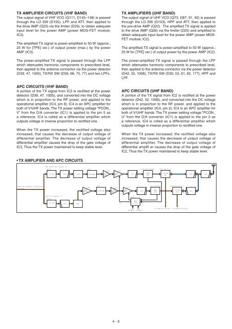
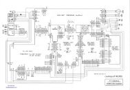
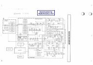
TX AMPLIFIER CIRCUITS (VHF BAND)The output signal of VHF VCO (Q111, D145–148) is passedthrough the LO SW (D155), LPF and ATT, then applied tothe drive AMP (Q25) via the limiter (D29), to obtain adequateinput level for the power AMP (power MOS-FET module;IC3).The amplifi ed TX signal is power-amplifi ed to 50 W (approx.;25 W for [TPE] ver.) of output power (max.) by the powerAMP (IC3).The power-amplified TX signal is passed through the LPFwhich attenuates harmonic components to prescribed level,then applied to the antenna connector via the power detector(D39, 47, 1005), TX/RX SW (D59, 68, 75, 77) and two LPFs.APC CIRCUITS (VHF BAND)A portion of the TX signal from IC3 is rectifi ed at the powerdetector (D39, 47, 1005), and converted into the DC voltagewhich is in proportion to the RF power, and applied to theoperational amplifi er (IC4, pin 6). IC4 is an APC amplifi er forboth of V/UHF bands. The TX power setting voltage “PCON_V” from the D/A converter (IC1) is applied to the pin 5 asa reference. IC4 is rolled as a differential amplifier whichoutputs voltage in inverse proportion to rectifi ed one.When the TX power increased, the rectified voltage alsoincreased, that causes the decrease of output voltage ofdifferential amplifier. The decrease of output voltage ofdifferential amplifi er causes the drop of the gate voltage ofIC3, Thus the TX power maintained to keep stable level.TX AMPLIFIERS (UHF BAND)The output signal of UHF VCO (Q73, D87, 91, 92) is passedthrough the LO SW (D103), HPF and ATT, then applied tothe pre-drive AMP (Q22). The amplifi ed TX signal is appliedto the drive AMP (Q26) via the limiter (D25) and amplifi ed toobtain adequate input level for the power AMP (power MOS-FET module; IC2).The amplifi ed TX signal is power-amplifi ed to 50 W (approx.;25 W for [TPE] ver.) of output power by the power AMP (IC2).The power-amplified TX signal is passed through the LPFwhich attenuates harmonic components to prescribed level,then applied to the antenna connector via the power detector(D42, 52, 1006), TX/RX SW (D30, 53, 61, 62, 177), HPF andLPF.APC CIRCUITS (UHF BAND)A portion of the TX signal from IC2 is rectifi ed at the powerdetector (D42, 52, 1006), and converted into the DC voltagewhich is in proportion to the RF power, and applied to theoperational amplifi er (IC4, pin 2). IC4 is an APC amplifi er forboth of V/UHF bands. The TX power setting voltage “PCON_U” from the D/A converter (IC1) is applied to the pin 3 asa reference. IC4 is rolled as a differential amplifier whichoutputs voltage in inverse proportion to rectifi ed one.When the TX power increased, the rectified voltage alsoincreased, that causes the decrease of output voltage ofdifferential amplifier. The decrease of output voltage ofdifferential amplifi er causes the drop of the gate voltage ofIC2, Thus the TX power maintained to keep stable level.• TX AMPLIFIER AND APC CIRCUITSVHF band TX signal ->D155LO SWLPFATTD29LIMITERQ25DRIVEAMPPWRAM PIC3LPFD39,D47,D1005PWRDETD59,68,75,77TX/RXSWLPFLPFFrom the frequency synthesizercircuitsPREDRIVEQ22D25LIMITERDRIVEAMPQ26PWRAM PIC2LPFD42,52,1006PWRDETD30,53,61,62,177TX/RXSWHPFUHF TX signal ->D103LO SWHPFATTTIC4APCCTRLPCON_UPCON_VTo VHF RX circuitsTo UHF RX circuits4 - 5
4-3 FREQUENCY SYNTHESIZERVCOsVHF VCOThe VHF VCO is composed by the oscillator circuit (Q111,D145, 146, 147) and buffer AMP (Q113), and generatesboth of 1st LO signals and TX signal for VHF band.The VCO oscillating signals are buffer-amplified by Q113,amplified by the LO AMP (IC45) to obtain adequate LO level,then applied to the TX amplifi ers or 1st IF mixer via the LOSW, ATT and fi lter.While transmitting;The VCO output signals from the LO AMP (IC45) are appliedto the TX amplifi ers via the LO SW (D155) as the TX signal.While receiving;The VCO output signals from the LO AMP (IC45) are passedthrough the LO SW (D170), ATT and the LPF, then applied tothe 1st IF mixer (Q124), as the 1st LO signals for 140 MHzband.The VCO output signals from the LO AMP (IC45) are passedthrough the LO SW (D104), ATT, RF SW and LPF, thenapplied to the 1st IF mixer (Q125), as the 1st LO signals for300 MHz band.UHF VCOThe UHF VCO is composed by the oscillator circuit (Q73,D87, 91, 92) and buffer AMP (Q76), and generates both of1st LO signals and TX signal for UHF band.The VCO oscillating signals are buffer-amplified by Q76,amplified by the LO AMP (IC45) to obtain adequate LO level,then applied to the TX amplifi ers or 1st IF mixer via the LOSW, ATT and fi lter.While transmitting;The VCO output signals from the LO AMP (IC45) are appliedto the TX amplifi ers via the LO SW (D103) as the TX signal.While receiving;The VCO output signals from the LO AMP (IC45) are passedthrough the LO SW (D101), ATT, doubler (HPF) and LPF,then applied to the 1st IF mixer (IC64), as the 1st LO signalsfor 800 MHz band.The VCO output signals from the LO AMP (IC45) are passedthrough the LO SW (D179), ATT and the LPF, then applied tothe 1st IF mixer (IC64), as the 1st LO signals for 440 MHz band.PLLThe PLL circuit provides stable oscillation of the transmitfrequency and receive 1st LO frequency. The PLL outputfrequency is controlled by control signals including divideratio (“PLLCK,”"PLLDATA”and "PLLSTB") from the CPU(IC25).PLL (VHF VCO)A portion of VHF VCO output signals from the buffer(Q113) are applied to the PLL IC (IC14) via the VCO switch(D175). The applied signals are divided at the prescaler andprogrammable counter.The divided signal is phase-compared with the 15.3 MHzreference frequency signal from the reference frequencyoscillator (X5), at the phase detector.The phase difference is output from pin 5 as a pulse typesignal after being passed through the internal charge pump.The output signal is converted into the DC voltage (lockvoltage) by passing through the loop fi lter (R694-698, C759-763). The lock voltage is applied to the variable capacitors(D145, 146), and locked to keep the VCO frequencyconstant.PLL (UHF VCO)A portion of VHF VCO output signals from the buffer (Q76)are applied to the PLL IC (IC14) via the VCO switch (Q1015).The applied signals are divided at the prescaler andprogrammable counter.The divided signal is phase-compared with the 15.3 MHzreference frequency signal from the reference frequencyoscillator (X5), at the phase detector.The phase difference is output from pins 15 and 16, andpassed through the external charge pump (Q61, 62) to beconverted into the pulse type signal.The output signal is converted into the DC voltage (lockvoltage) by passing through the loop fi lter (R355, 362, 365,369, 378, C451, 456, 473). The lock voltage is applied to thevariable capacitors (D91, 92), and locked to keep the VCOfrequency constant.• FREQUENCY SYNTHESIZER CIRCUITSD155LO SWTo VHF TX AamplifierD103LO SWTo UHF TX AamplifierPLLCKPLLDATAPLLSTBX515.3MHzTCXOLOOPFILIC14PLLICQ5245.9 MHzX3IF ICIC15IC1018VCOSELECTQ61,62LOOPFILVHF VCOQ110,111D145-148UHF VCOQ73D87,91,92Q113BUFFQ76BUFFD160,D175VCOSWQ 1015BUFFVCOSWD102LOAMPIC45D170LO SWATTATTATTATTX2(HPF)LPF-> RX LO signals for 140 MHz band (118-174 MHz) ->D179LO SWLPF-> RX LO signals for 440 MHz band (420-550 MHz) ->D101LO SWLPF-> RX LO signals for 800MHz band (810-999 MHz) ->D104Q79D180LO SWRFSWLPF-> RX LO signals for 300 MHz band (230-420 MHz) ->D181LO SWLO SWQ124140 MHz band1st IF MIXERQ125440 MHz band1st IF MIXERIC64800 MHz and300 MHz bands1st IF MIXER4 - 6