Microring and microdisk resonator integrated circuits on a silicon chip
Microring and microdisk resonator integrated circuits on a silicon chip
Microring and microdisk resonator integrated circuits on a silicon chip

You also want an ePaper? Increase the reach of your titles
YUMPU automatically turns print PDFs into web optimized ePapers that Google loves.
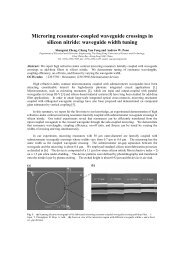
us waveguide with the carrier wavelength at the microring notch filter wavelength λ 0 . After passing through the notchfilter, the NRZ signal is c<strong>on</strong>verted to a PRZ signal by suppressing the optical carrier frequency comp<strong>on</strong>ents <str<strong>on</strong>g>and</str<strong>on</strong>g>effectively enhancing the optical clock comp<strong>on</strong>ents in the notch filter transmissi<strong>on</strong>. In time domain, the transmissi<strong>on</strong>signal appears as discrete PRZ pulses corresp<strong>on</strong>ding to the transiti<strong>on</strong> edges of the NRZ signal, as shown in Fig. 1(b).Fig. 2. (a) Optical micrograph of an actively tunable racetrack microring <str<strong>on</strong>g>res<strong>on</strong>ator</str<strong>on</strong>g> notch filter with laterally <str<strong>on</strong>g>integrated</str<strong>on</strong>g> p-i-n diode <strong>on</strong>an SOI substrate. Inset: cross-secti<strong>on</strong>al schematic of the p-i-n diode. (b) Measured TE-polarized throughput-port spectrum up<strong>on</strong>various forward biases. (c) – (f) Measured transmissi<strong>on</strong> of a 3.6-Gbps NRZ signal at (c) an off-res<strong>on</strong>ance carrier wavelength (1546nm, cyan line), (d) an <strong>on</strong>-res<strong>on</strong>ance carrier wavelength under 0-V forward bias (1546.9 nm, blue line), (e) an <strong>on</strong>-res<strong>on</strong>ance carrierwavelength under 1.2-V forward bias (1546.15 nm, red line), <str<strong>on</strong>g>and</str<strong>on</strong>g> (f) an <strong>on</strong>-res<strong>on</strong>ance carrier wavelength under 1.4-V forward bias(1545.68 nm, yellow line).Figure 2(a) shows an optical micrograph of our fabricated racetrack microring <str<strong>on</strong>g>res<strong>on</strong>ator</str<strong>on</strong>g>-based notch filter with laterally<str<strong>on</strong>g>integrated</str<strong>on</strong>g> p-i-n diode surrounding most of the microring <strong>on</strong> a silic<strong>on</strong>-<strong>on</strong>-insulator (SOI) substrate. The fabricati<strong>on</strong>employs i-line optical lithography <str<strong>on</strong>g>and</str<strong>on</strong>g> dry etching as in our previous work [27]. The <str<strong>on</strong>g>integrated</str<strong>on</strong>g> diode enables active EOtuning in order to match the notch filter wavelength with the signal carrier wavelength. The racetrack arc radius is 25µm <str<strong>on</strong>g>and</str<strong>on</strong>g> the straight interacti<strong>on</strong> length is 10 µm. Inset shows the cross-secti<strong>on</strong>al schematic of the laterally <str<strong>on</strong>g>integrated</str<strong>on</strong>g> p-indiode. The rib waveguide in the intrinsic regi<strong>on</strong> has a width of 0.4 µm, a height of 0.21 µm, <str<strong>on</strong>g>and</str<strong>on</strong>g> an etched depth of0.18 µm. The p + -doped (2x10 19 cm -3 ) <str<strong>on</strong>g>and</str<strong>on</strong>g> n + -doped (1x10 20 cm -3 ) regi<strong>on</strong>s are positi<strong>on</strong>ed in the slab layer, with ~0.5-µmseparati<strong>on</strong>s from the waveguide sidewalls.Figure 2(b) shows the measured TE-polarized (electric field in the device plane) transmissi<strong>on</strong> spectra with the p-i-ndiode forward biased at 0 V, 1.0 V, 1.2 V, <str<strong>on</strong>g>and</str<strong>on</strong>g> 1.4 V. Under 0-V bias, the transmissi<strong>on</strong> dip (Q ~ 5,000) <strong>on</strong>ly exhibits anextincti<strong>on</strong> ratio (ER) of ~6 dB. As the diode is gradually forward biased (bey<strong>on</strong>d the threshold voltage of ~0.75 V), thecarrier-induced res<strong>on</strong>ance wavelength blueshift <str<strong>on</strong>g>and</str<strong>on</strong>g> the ER increases with forward biases until reaching an optimum at~18 dB up<strong>on</strong> a 1.2-V bias, suggesting a transiti<strong>on</strong> from over-coupling to critical coupling regimes.Figures 2(c) – 2(f) show the measured 3.6-Gbps NRZ signal transmissi<strong>on</strong> waveforms at an off-res<strong>on</strong>ance wavelength (0-V bias) <str<strong>on</strong>g>and</str<strong>on</strong>g> at <strong>on</strong>-res<strong>on</strong>ance wavelengths up<strong>on</strong> forward biases at 0 V, 1.2 V, <str<strong>on</strong>g>and</str<strong>on</strong>g> 1.4 V. The off-res<strong>on</strong>ance waveformlargely follows the input NRZ signal (except for the ripples observed in the optical waveform). The optical signaldisplays a rise time of ~30 ps <str<strong>on</strong>g>and</str<strong>on</strong>g> a fall time of ~35 ps. The <strong>on</strong>-res<strong>on</strong>ance waveform up<strong>on</strong> 1.2-V bias displays PRZpulses following the transiti<strong>on</strong> edges with pulse widths of ~36 ps <str<strong>on</strong>g>and</str<strong>on</strong>g> a peak extincti<strong>on</strong> ratio of ~6 dB for the rising edgepulses. The shorter NRZ signal rise time gives rise to higher PRZ pulse amplitudes. Whereas, the <strong>on</strong>-res<strong>on</strong>ancewaveform up<strong>on</strong> 0-V (1.4-V) bias displays a distorted NRZ signal, with an overshoot at the signal falling (rising) edge<str<strong>on</strong>g>and</str<strong>on</strong>g> a dip followed with a slight peak at the signal rising (falling) edge. We note that the relatively low ERs (< 10 dB)up<strong>on</strong> 0-V <str<strong>on</strong>g>and</str<strong>on</strong>g> 1.4-V biases render less optical carrier suppressi<strong>on</strong> <str<strong>on</strong>g>and</str<strong>on</strong>g> thereby less pr<strong>on</strong>ounced clock comp<strong>on</strong>ents.3. SILICON MICRORING ELECTRO-OPTIC MODULATORS WITH EXTERNAL FEEDBACKIn this secti<strong>on</strong>, we extend our actively tunable silic<strong>on</strong> microring notch filter work to an actively rec<strong>on</strong>figurable EOmodulator. We propose <str<strong>on</strong>g>and</str<strong>on</strong>g> initially dem<strong>on</strong>strate a silic<strong>on</strong> microring EO modulator that can be actively tuned by meansof an external feedback. The c<strong>on</strong>cept is based <strong>on</strong> our previous work <strong>on</strong> silic<strong>on</strong> microring notch filter comprising amicroring that is double-coupled to a U-bend waveguide [35]. Here as a modulator, both the microring <str<strong>on</strong>g>and</str<strong>on</strong>g> the feedback