Microring and microdisk resonator integrated circuits on a silicon chip
Microring and microdisk resonator integrated circuits on a silicon chip
Microring and microdisk resonator integrated circuits on a silicon chip

Create successful ePaper yourself
Turn your PDF publications into a flip-book with our unique Google optimized e-Paper software.
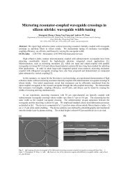
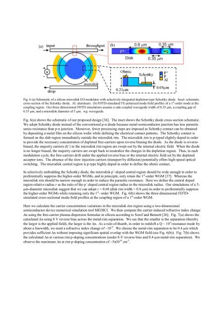
Fig. 6 (a) Schematic of a silic<strong>on</strong> <str<strong>on</strong>g>microdisk</str<strong>on</strong>g> EO modulator with selectively <str<strong>on</strong>g>integrated</str<strong>on</strong>g> depleti<strong>on</strong>-type Schottky diode. Inset: schematiccross-secti<strong>on</strong> of the Schottky diode. Al: aluminum. (b) FDTD-simulated TE-polarized mode-field profiles of a 1 st -order mode at thecoupling regi<strong>on</strong>. Our three-dimensi<strong>on</strong>al FDTD simulati<strong>on</strong>s assume a side-coupled waveguide width of 0.35 µm, a coupling gap of0.35 µm, <str<strong>on</strong>g>and</str<strong>on</strong>g> a <str<strong>on</strong>g>microdisk</str<strong>on</strong>g> diameter of 5 µm. wg: waveguide.Fig. 6(a) shows the schematic of our proposed design [36]. The inset shows the Schottky diode cross-secti<strong>on</strong> schematic.We adopt Schottky diode instead of the c<strong>on</strong>venti<strong>on</strong>al p-n diode because metal-semic<strong>on</strong>ductor juncti<strong>on</strong> has less parasiticseries resistance than p-n juncti<strong>on</strong>. Moreover, fewer processing steps are imposed as Schottky c<strong>on</strong>tact can be obtainedby depositing a metal film <strong>on</strong> the silic<strong>on</strong> wafer while defining the electrical c<strong>on</strong>tact patterns. The Schottky c<strong>on</strong>tact isformed <strong>on</strong> the slab regi<strong>on</strong> immediately outside the <str<strong>on</strong>g>microdisk</str<strong>on</strong>g> rim. The <str<strong>on</strong>g>microdisk</str<strong>on</strong>g> rim is p-typed slightly doped in orderto provide the necessary c<strong>on</strong>centrati<strong>on</strong> of depleted free-carriers up<strong>on</strong> reverse biasing the diode. As the diode is reversebiased,the majority carriers (h + ) in the <str<strong>on</strong>g>microdisk</str<strong>on</strong>g> rim regi<strong>on</strong> are swept out by the internal electric field. When the diodeis no l<strong>on</strong>ger biased, the majority carriers are swept back to neutralize the charges in the depleti<strong>on</strong> regi<strong>on</strong>. Thus, in eachmodulati<strong>on</strong> cycle, the free-carriers drift under the applied reverse bias or the internal electric field set by the depletedacceptor i<strong>on</strong>s. The absence of the slow injecti<strong>on</strong> carriers (transport by diffusi<strong>on</strong>) potentially offers high-speed opticalswitching. The <str<strong>on</strong>g>microdisk</str<strong>on</strong>g> central regi<strong>on</strong> is p-type highly doped in order to define the ohmic c<strong>on</strong>tact.In selectively embedding the Schottky diode, the <str<strong>on</strong>g>microdisk</str<strong>on</strong>g> p + -doped central regi<strong>on</strong> should be wide enough in order topreferentially suppress the higher-order WGMs, <str<strong>on</strong>g>and</str<strong>on</strong>g> in principle, <strong>on</strong>ly retain the 1 st -order WGM [37]. Whereas the<str<strong>on</strong>g>microdisk</str<strong>on</strong>g> rim should be narrow enough in order to reduce the parasitic resistance. Here we define the central dopedregi<strong>on</strong> relative radius r as the ratio of the p + -doped central regi<strong>on</strong> radius to the <str<strong>on</strong>g>microdisk</str<strong>on</strong>g> radius. Our simulati<strong>on</strong>s of a 5-µm-diameter <str<strong>on</strong>g>microdisk</str<strong>on</strong>g> suggest that we can adopt r = 0.68 (disk rim width = 0.8 µm) in order to preferentially suppressthe higher-order WGMs while retaining <strong>on</strong>ly the 1 st - order WGM. Fig. 6(b) shows the three-dimensi<strong>on</strong>al FDTDsimulatedcross-secti<strong>on</strong>al mode-field profiles at the coupling regi<strong>on</strong> of a 1 st -order WGM.Here we calculate the carrier c<strong>on</strong>centrati<strong>on</strong> variati<strong>on</strong>s in the <str<strong>on</strong>g>microdisk</str<strong>on</strong>g> rim regi<strong>on</strong> using a two-dimensi<strong>on</strong>alsemic<strong>on</strong>ductor device numerical simulati<strong>on</strong> tool MEDICI. We then compute the carrier-induced refractive index change∆n using the free-carrier plasma dispersi<strong>on</strong> formulae in silic<strong>on</strong> according to Soref <str<strong>on</strong>g>and</str<strong>on</strong>g> Bennett [26]. Fig. 7(a) shows thecalculated ∆n using 8 V reverse bias across the metal-rim separati<strong>on</strong>. We see that the smaller is the separati<strong>on</strong> (therebythe larger is the applied field), the larger is the ∆n. As a rule-of-thumb, in order to redshift a Q ~ 10 4 res<strong>on</strong>ance mode byabout a linewidth, we need a refractive index change of ~10 -4 . We choose the metal-rim separati<strong>on</strong> to be 0.4 µm whichprovides sufficient ∆n without imposing significant spatial overlap with the WGM field (see Fig. 6(b)). Fig. 7(b) showsthe calculated ∆n at various rim p-doping c<strong>on</strong>centrati<strong>on</strong>s (under 8-V reverse bias <str<strong>on</strong>g>and</str<strong>on</strong>g> 0.4-µm metal-rim separati<strong>on</strong>). Weobserve the maximum ∆n at rim p-doping c<strong>on</strong>centrati<strong>on</strong> of ~5x10 16 cm -3 .